

Page 1
查询HY29F080供应商
KEY FEATURES
HY29F080
8 Megabit (1M x 8), 5 Volt-only, Flash Memory
n 5 Volt Read, Program, and Erase
– Minimizes system-level power
requirements
n High Performance
– Access times as fast as 70 ns
n Low Power Consumption
– 15 mA typical active read current
– 30 mA typical program/erase current
– 5 µA maximum CMOS standby current
n Compatible with JEDEC Standards
– Package, pinout and command-set
compatible with the single-supply Flash
device standard
– Provides superior inadvertent write
protection
n Sector Erase Architecture
– Sixteen equal size sectors of 64K bytes
each
– A command can erase any combination of
sectors
– Supports full chip erase
n Erase Suspend/Resume
– Temporarily suspends a sector erase
operation to allow data to be read from, or
programmed into, any sector not being
erased
n Sector Group Protection
– Sectors may be locked in groups of two to
prevent program or erase operations
within that sector group
n Temporary Sector Unprotect
– Allows changes in locked sectors
(requires high voltage on RESET# pin)
n Internal Erase Algorithm
– Automatically erases a sector, any
combination of sectors, or the entire chip
n Internal Programming Algorithm
– Automatically programs and verifies data
at a specified address
n Fast Program and Erase Times
– Byte programming time: 7 µs typical
– Sector erase time: 1.0 sec typical
– Chip erase time: 16 sec typical
n Data# Polling and Toggle Status Bits
– Provide software confirmation of
completion of program or erase
operations
n Ready/Busy# Pin
– Provides hardware confirmation of
completion of program and erase
operations
n Minimum 100,000 Program/Erase Cycles
n Space Efficient Packaging
– Available in industry-standard 40-pin
TSOP and 44-pin PSOP packages
GENERAL DESCRIPTION
The HY29F080 is an 8 Megabit, 5 volt-only CMOS
Flash memory organized as 1,048,576 (1M) bytes
of eight-bits each. The device is offered in industry-standard 44-pin PSOP and 40-pin TSOP packages.
The HY29F080 can be programmed and erased
in-system with a single 5-volt V
supply. Inter-
CC
nally generated and regulated voltages are provided for program and erase operations, so that
the device does not require a high voltage power
supply to perform those functions. The device can
also be programmed in standard EPROM programmers. Access times as fast as 70ns over the
full operating voltage range of 5.0 volts ± 10% are
offered for timing compatibility with the zero wait
state requirements of high speed microprocessors.
Revision 6.1, May 2001
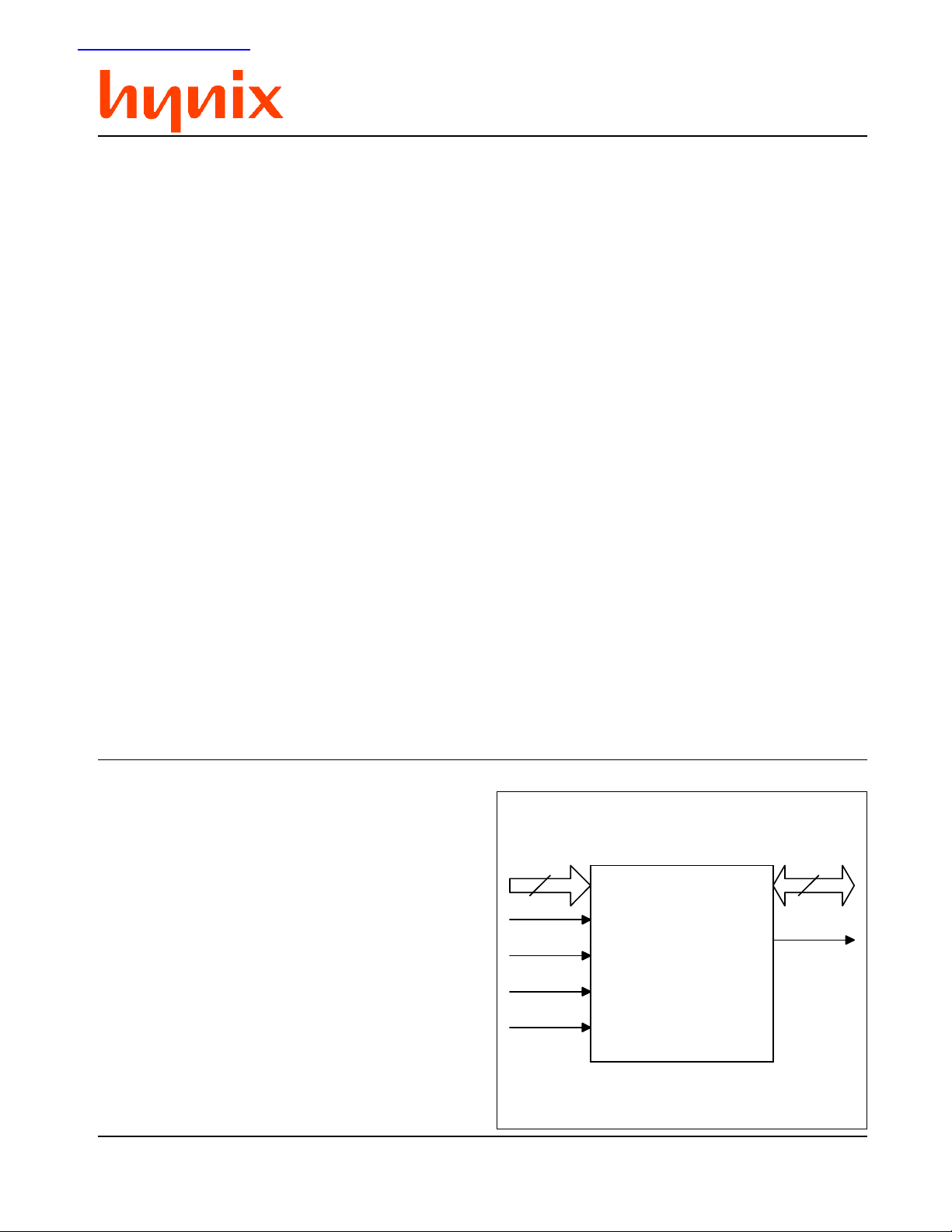
LOGIC DIAGRAM
20
A[19:0]
RESET#
CE#
OE#
WE#
8
DQ[7:0]
RY/BY#
Page 2
HY29F080
To eliminate bus contention, the HY29F080 has
separate chip enable (CE#), write enable (WE#)
and output enable (OE#) controls.
The device is compatible with the JEDEC single
power-supply Flash command set standard. Commands are written to the command register using
standard microprocessor write timings, from where
they are routed to an internal state-machine that
controls the erase and programming circuits.
Device programming is performed a byte at a time
by executing the four-cycle Program Command.
This initiates an internal algorithm that automatically times the program pulse widths and verifies
proper cell margin.
The HY29F080’s sector erase architecture allows
any number of array sectors to be erased and reprogrammed without affecting the data contents
of other sectors. Device erasure is initiated by
executing the Erase Command. This initiates an
internal algorithm that automatically preprograms
the array (if it is not already programmed) before
executing the erase operation. During erase
cycles, the device automatically times the erase
pulse widths and verifies proper cell margin.
the device has a Sector Group Protect function
which hardware write protects selected sector
groups. The sector group protect and unprotect
features can be enabled in a PROM programmer.
Temporary Sector Unprotect, which requires a high
voltage, allows in-system erasure and code
changes in previously protected sectors.
Erase Suspend enables the user to put erase on
hold for any period of time to read data from, or
program data to, any sector that is not selected
for erasure. True background erase can thus be
achieved. The device is fully erased when shipped
from the factory.
Addresses and data needed for the programming
and erase operations are internally latched during
write cycles, and the host system can detect
completion of a program or erase operation by
observing the RY/BY# pin, or by reading the DQ[7]
(Data# Polling) and DQ[6] (toggle) status bits.
Reading data from the device is similar to reading
from SRAM or EPROM devices. Hardware data
protection measures include a low V
detector
CC
that automatically inhibits write operations during
power transitions.
To protect data in the device from accidental or
unauthorized attempts to program or erase the
device while it is in the system (e.g., by a virus),
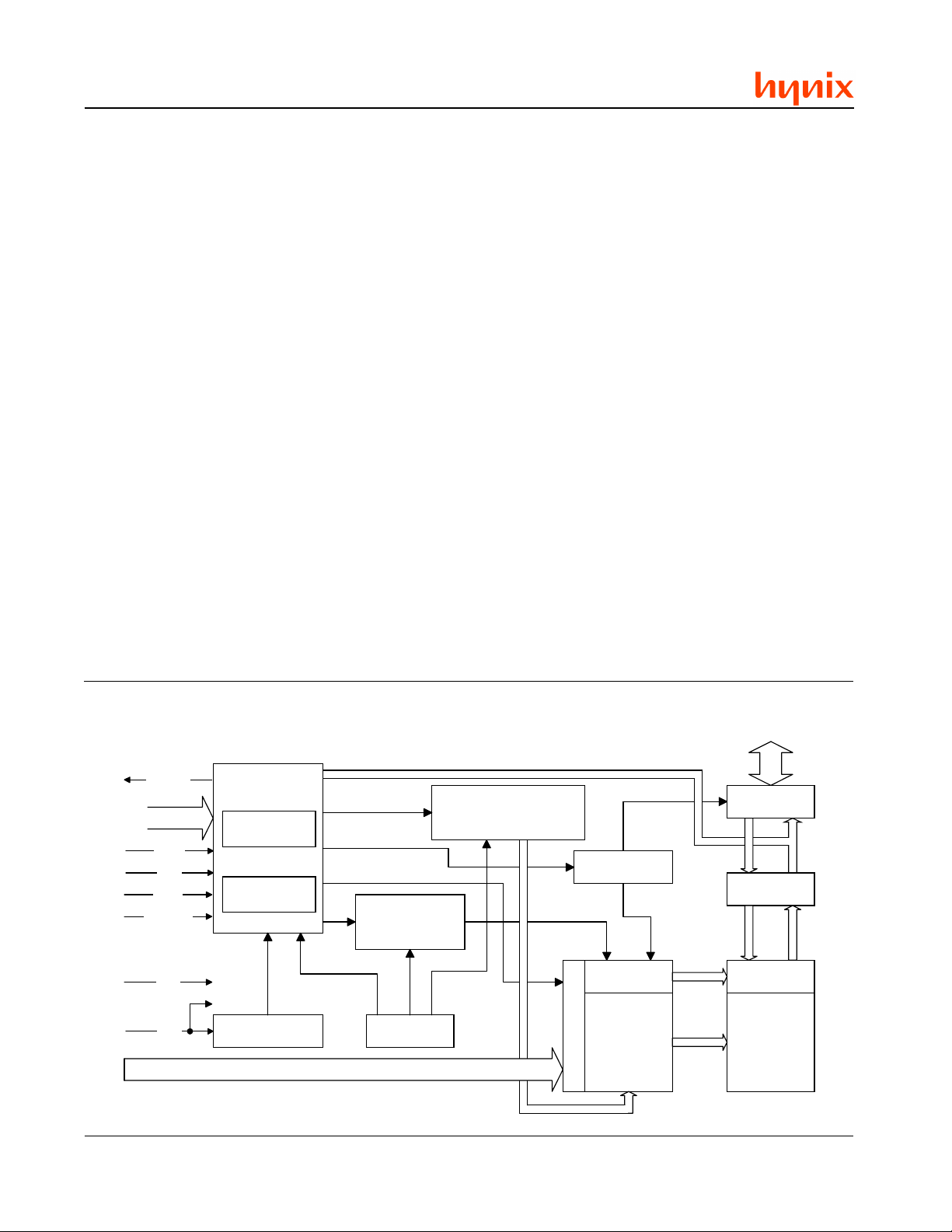
BLOCK DIAGRAM
RY/BY#
DQ[7:0]
WE#
CE#
OE#
RESET#
V
V
A[19:0]
SS
CC
STATE
CONTROL
COMMAND
REGISTER
ELECTRONIC
ID
VCC DETECTOR TIMER
PROGRAM
VOLTAGE
GENERATOR
The host can place the device into the standby
mode. Power consumption is greatly reduced in
this mode.
DQ[7:0]
ERASE VOLTAGE
GENERATOR AND
SECTOR SWITCHES
I/O CONTROL
Y-DECODER
X-DECODER
ADDRESS LATCH
I/O BUFFERS
DATA LATCH
Y-GATING
8 Mbit FLASH
MEMORY
ARRAY
(16 x 512 Kbit
Sectors)
2
Rev. 6.1/May 01
Page 3
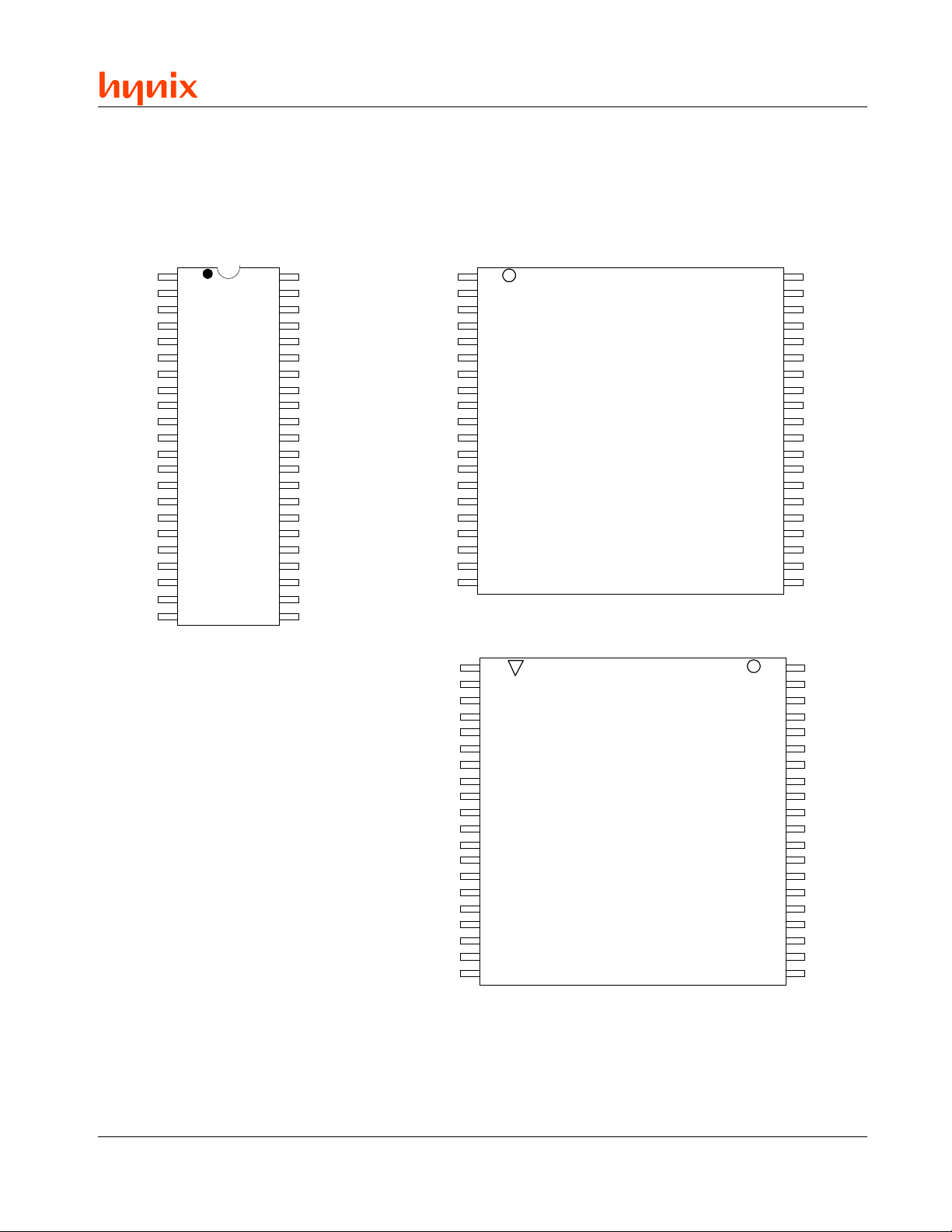
PIN CONFIGURATIONS
HY29F080
NC
RESET#12
A11
A10
A9
A8
A7
A6
A5
A4910
NC
NC1112
A3
A21314
A1
A01516
DQ0
DQ11718
DQ2
DQ31920
V
V
21
SS
22
SS
3
4
5
6
7
8
PSOP44
44
43
42
41
40
39
38
37
36
35
34
33
32
31
30
29
28
27
26
25
24
23
V
CC
CE#
A12
A13
A14
A15
A16
A17
A18
A19
NC
NC
NC
NC
WE#
OE#
RY/BY#
DQ7
DQ6
DQ5
DQ4
V
CC
A19
A18
A17
A16
A15
A14
A13
A12
CE#
V
NC
RESET#1112
A11
A101314
WE#
OE#
RY/BY#
DQ7
DQ6
DQ5
DQ4
V
V
V
DQ3
DQ21314
DQ1
DQ01516
10
CC
A9
A81516
A7
A61718
A5
A41920
NC
NC
10
CC
11
SS
12
SS
A0
A11718
A2
A31920
NC
1
2
3
4
5
6
7
8
9
Standard
TSOP40
1
2
3
4
5
6
7
8
9
Reverse
TSOP40
40
39
38
37
36
35
34
33
32
31
30
29
28
27
26
25
24
23
22
21
40
39
38
37
36
35
34
33
32
31
30
29
28
27
26
25
24
23
22
21
NC
WE#
OE#
RY/BY#
DQ7
DQ6
DQ5
DQ4
V
CC
V
SS
V
SS
DQ3
DQ2
DQ1
DQ0
A0
A1
A2
A3
A19
A18
A17
A16
A15
A14
A13
A12
CE#
V
CC
NC
RESET#
A11
A10
A9
A8
A7
A6
A5
A4
Rev. 6.1/May 01
3
Page 4

HY29F080
CONVENTIONS
Unless otherwise noted, a positive logic (active
High) convention is assumed throughout this document, whereby the presence at a pin of a higher,
more positive voltage (nominally 5VDC) causes
assertion of the signal. A ‘#’ symbol following the
signal name, e.g., RESET#, indicates that the signal is asserted in a Low state (nominally 0 volts).
SIGNAL DESCRIPTIONS
emaN epyT noitpircseD
]0:91[AstupnI
.BSL
]0:7[QD
#ECtupnI
#EOtupnI
#EWtupnI
#TESERtupnI
#YB/YR
V
CC
V
SS
MEMORY ARRAY ORGANIZATION
The 1 MByte Flash memory array is organized into
sixteen 64 KByte blocks called sectors (S0, S1, . .
. , S15). A sector is the smallest unit that can be
erased. Adjacent pairs of sectors (S0/S1, S2/S3,
. . . , S14/S15) are designated as a sector group.
A sector group is the smallest unit which can be
protected to prevent accidental or unauthorized
stuptuO/stupnI
etats-irT
tuptuO
niarDnepO
--
--
.snoitarepo
.hgiHsi
.atadyarra
Whenever a signal is separated into numbered
bits, e.g., DQ[7], DQ[6], ..., DQ[0], the family of
bits may also be shown collectively, e.g., as
DQ[7:0].
The designation 0xNNNN (N = 0, 1, 2, . . . , 9, A, .
. . , E, F) indicates a number expressed in hexadecimal notation. The designation 0bXXXX indicates a number expressed in binary notation (X =
0, 1).
.hgiHevitca,sserddA setyb)M1(675,840,1foenotcelesstupniytnewtesehT
ehtsi]0[AdnaBSMehtsi]91[A.snoitarepoetirwrodaerrofyarraehtnihtiw
hgiHevitca,suBataD etirwdnadaerrofhtapatadtib-8naedivorpsnipesehT.
.woLevitca,elbanEpihC romorfataddaerotdetressaebtsumtupnisihT
ecivedehtdnadetats-irtsisubatadeht,hgiHnehW.080F92YHehtotatadetirw
.edomybdnatSehtnidecalpsi
woLevitca,elbanEtuptuO snoitarepodaerrofdetressaebtsumtupnisihT.
eraecivedehtmorfstuptuoatad,hgiHnehW.snoitarepoetirwrofdetagendna
.etatsecnadepmihgihehtnidecalperasnipsubatadehtdnadelbasid
.woLevitca,elbanEetirW dnammocrosdnammocfognitirwslortnoC
A.yarrayromemehtfosrotcesesareroatadmargorpotredronisecneuqes
#EOdnawoLsi#ECelihwdetressasi#EWnehwecalpsekatnoitarepoetirw
.woLevitca,teseRerawdraH ehtgnitteserfodohtemerawdrahasedivorP
yletaidemmiti,tesersiecivedehtnehW.etatsyarradaerehtot080F92YH
etirw/daerlladnadetats-irtsisubatadehT.ssergorpninoitarepoynasetanimret
,detressasi#TESERelihW.detressasitupniehtelihwderongierasdnammoc
.edomybdnatSehtnieblliwecivedeht
.sutatSysuB/ydaeR nisidnammocesareroetirwarehtehwsetacidnI
ehtfoegdegnisirehtretfadilavsi#YB/YR.detelpmocneebsahrossergorp
siecivedehtelihwwoLsniamertI.ecneuqesdnammocafoeslup#EWlanif
daerotydaersitinehwhgiHseogdna,gnisareroatadgnimmargorpylevitca
.ylppusrewoptlov-5
.dnuorglangisdnarewoP
erasure. See ‘Bus Operations’ and ‘Command
Definitions’ sections of this document for additional
information on these functions.
Table 1 defines the sector addresses, sector group
addresses and corresponding address ranges for
the HY29F080.
4
Rev. 6.1/May 01
Page 5
Table 1. HY29F080 Memory Array Organization
1
rotceS
0S
1S 0001 FFFF1x0-00001x0
2S
3S0011 FFFF3x0-00003x0
4S
5S0101 FFFF5x0-00005x0
6S
7S 0111 FFFF7x0-00007x0
8S
9S1001 FFFF9x0-00009x0
01S
11S1011 FFFFBx0-0000Bx0
21S
31S1101 FFFFDx0-0000Dx0
41S
51S 1111 FFFFFx0-0000Fx0
Notes:
1. A[19:16] are the sector address. A[19:17] are the sector group address.
rotceS
puorG
0GS
1GS
2GS
3GS
4GS
5GS
6GS
7GS
]91[A ]81[A ]71[A ]61[A
0000 FFFF0x0-00000x0
0010 FFFF2x0-00002x0
0100 FFFF4x0-00004x0
0110 FFFF6x0-00006x0
1000 FFFF8x0-00008x0
1010 FFFFAx0-0000Ax0
1100 FFFFCx0-0000Cx0
1110 FFFFEx0-0000Ex0
sserddApuorGrotceS/rotceS
HY29F080
]0:91[AegnaRsserddA
BUS OPERATIONS
Device bus operations are initiated through the
internal command register, which consists of sets
of latches that store the commands, along with
the address and data information, if any, needed
to execute the specific command. The command
register itself does not occupy any addressable
memory location. The contents of the command
Table 2. HY29F080 Normal Bus Operations
noitarepO #EC #EO #EW #TESER ]0:91[A ]0:7[QD
daeRLLHHA
etirWLHLHA
elbasiDtuptuOLHHHXZ-hgiH
ybdnatSLTT#ECHXXHXZ-hgiH
ybdnatSSOMC#ECV
)ybdnatSLTT(teseRerawdraHXXXLXZ-hgiH
)ybdnatSSOMC(teseRerawdraHXXXV
Notes:
1. L = VIL, H = VIH, X = Don’t Care, D
CC
= Data Out, DIN = Data In. See DC Characteristics for voltage levels.
OUT
1
V3.0±XXVCCV3.0±XZ-hgiH
register serve as inputs to an internal state machine whose outputs control the operation of the
device. Table 2 lists the normal bus operations,
the inputs and control levels they require, and the
resulting outputs. Certain bus operations require
a high voltage on one or more device pins. Those
are described in Table 3.
D
TUO
D
NI
V5.0±XZ-hgiH
SS
NI
NI
Rev. 6.1/May 01
5
Page 6

HY29F080
Table 3. HY29F080 Bus Operations Requiring High Voltage
3
noitarepO
#EC #EO #EW
-TESER
#
]71:91[A ]9[A ]6[A ]1[A ]0[A ]0:7[QD
1, 2
puorGrotceS
tcetorP
puorGrotceS
tcetorpnU
LV
V
DI
DI
V
DI
XH AGS
XH AGS
yraropmeT
puorGrotceS
XXX V
DI
tcetorpnU
rerutcafunaM
edoC
LLH H XV
edoCeciveDLLHHXV
puorGrotceS
noitcetorP
LLH H AGS
noitacifireV
Notes:
1. L = V
2. Address bits not specified are Don’t Care.
3. See text for additional information.
4. SGA = sector group address. See Table 1.
, H = VIH, X = Don’t Care. See DC Characteristics for voltage levels.
IL
Read Operation
Data is read from the HY29F080 by using standard microprocessor read cycles while placing the
address of the byte to be read on the device’s
address inputs, A[19:0]. As shown in Table 2, the
host system must drive the CE# and OE# inputs
Low and drive WE# High for a valid read operation to take place. The device outputs the specified array data on DQ[7:0].
The HY29F080 is automatically set for reading
array data after device power-up and after a hardware reset to ensure that no spurious alteration of
the memory content occurs during the power transition. No command is necessary in this mode to
obtain array data, and the device remains enabled
for read accesses until the command register contents are altered.
This device features an Erase Suspend mode.
While in this mode, the host may read the array
data from any sector of memory that is not marked
for erasure. If the host attempts to read from an
address within an erase-suspended sector, or
while the device is performing an erase or byte
program operation, the device outputs status data
4
V
DI
4
V
DI
XXX X
XXX X
X XXXX X
DI
DI
LLL DAx0=xinyH
LLH
=080F92YH
5Dx0
=00x0
4
V
DI
LHL
detcetorpnU
=10x0
detcetorP
instead of array data. After completing a programming operation in the Erase Suspend mode, the
system may once again read array data with the
same exceptions noted above. After completing
an internal program or internal erase algorithm,
the HY29F080 automatically returns to the read
array data mode.
The host must issue a hardware reset or the software reset command (see Command Definitions)
to return a sector to the read array data mode if
DQ[5] goes high during a program or erase cycle,
or to return the device to the read array data mode
while it is in the Electronic ID mode.
Write Operation
Certain operations, including programming data
and erasing sectors of memory, require the host
to write a command or command sequence to the
HY29F080. Writes to the device are performed
by placing the byte address on the device’s address inputs while the data to be written is input
on DQ[7:0]. The host system must drive the CE#
and WE# pins Low and drive OE# High for a valid
write operation to take place. All addresses are
6
Rev. 6.1/May 01
Page 7

HY29F080
latched on the falling edge of WE# or CE#, whichever happens later. All data is latched on the rising edge of WE# or CE#, whichever happens first.
The ‘Device Commands’ section of this document
provides details on the specific device commands
implemented in the HY29F080.
Output Disable Operation
When the OE# input is at V
, output data from the
IH
device is disabled and the data bus pins are placed
in the high impedance state.
Standby Operation
When the system is not reading from or writing to
the HY29F080, it can place the device in the
Standby mode. In this mode, current consumption is greatly reduced, and the data bus outputs
are placed in the high impedance state, independent of the OE# input. The Standby mode can
invoked using two methods.
The device enters the CE# CMOS Standby mode
if the CE# and RESET# pins are both held at V
CC
± 0.5V. Note that this is a more restricted voltage
range than V
High, but not within V
. If both CE# and RESET# are held
IH
± 0.5V, the device will be
CC
in the CE# TTL Standby mode, but the standby
current will be greater.
The device enters the RESET# CMOS Standby
mode when the RESET# pin is held at V
If RESET# is held Low but not within V
± 0.5V.
SS
± 0.5V,
SS
the HY29F080 will be in the RESET# TTL Standby
mode, but the standby current will be greater. See
Hardware Reset Operation section for additional
information on the reset operation.
The device requires standard access time (t
CE
) for
read access when the device is in either of the
standby modes, before it is ready to read data. If
the device is deselected during erasure or programming, it continues to draw active current until
the operation is completed.
the duration of the RESET# pulse. The device also
resets the internal state machine to reading array
data. If an operation was interrupted by the assertion of RESET#, it should be reinitiated once
the device is ready to accept another command
sequence to ensure data integrity.
Current is reduced for the duration of the RESET#
pulse as described in the Standby Operation section above.
If RESET# is asserted during a program or erase
operation (RY/BY# pin is Low), the internal reset
operation is completed within a time of t
READY
(during
Automatic Algorithms). The RY/BY# pin will go High
during the t
interval, and the system can per-
READY
form a read or write operation after waiting for a minimum of t
or until tRH after the RESET# pin re-
READY
turns High, whichever is longer. If RESET# is asserted when a program or erase operation is not
executing (RY/BY# pin is High), the reset operation
is completed within a time of t
host can perform a read or write operation t
. In this case, the
RP
RH
after
the RESET# pin returns High.
The RESET# pin may be tied to the system reset
signal. Thus, a system reset would also reset the
device, enabling the system to read the boot-up
firmware from the Flash memory.
Sector Group Protect/Unprotect Operations
Hardware sector group protection can be invoked
to disable program and erase operations in any
single sector group or combination of sector
groups. This function is typically used to protect
data in the device from unauthorized or accidental attempts to program or erase the device while
it is in the system (e.g., by a virus) and is implemented using programming equipment. Sector
group unprotection re-enables the program and
erase operations in previously protected sectors.
Table 1 identifies the eight sector groups and the
address ranges that each covers. The device is
shipped with all sector groups unprotected.
Hardware Reset Operation
The RESET# pin provides a hardware method of
resetting the device to reading array data. When
the RESET# pin is driven Low for the minimum
specified period, the device immediately terminates any operation in progress, tri-states the data
bus pins, and ignores all read/write commands for
Rev. 6.1/May 01
The sector group protect/unprotect operations require a high voltage (V
) on address pin A9 and
ID
the CE# and/or OE# control pins, as detailed in
Table 3. When implementing these operations,
note that V
applying V
fore removing V
must be applied to the device before
CC
, and that VID should be removed be-
ID
from the device.
CC
7
Page 8
HY29F080
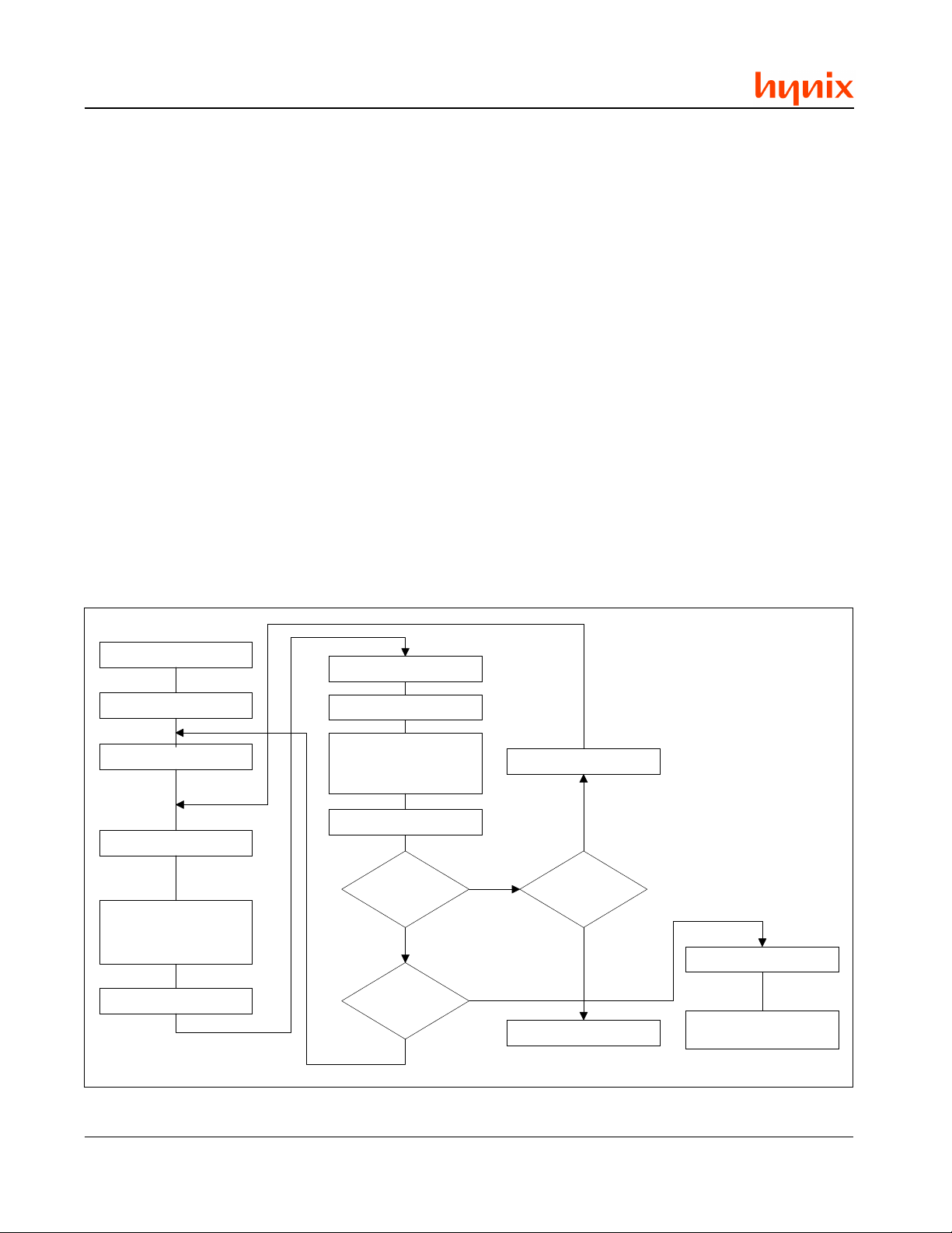
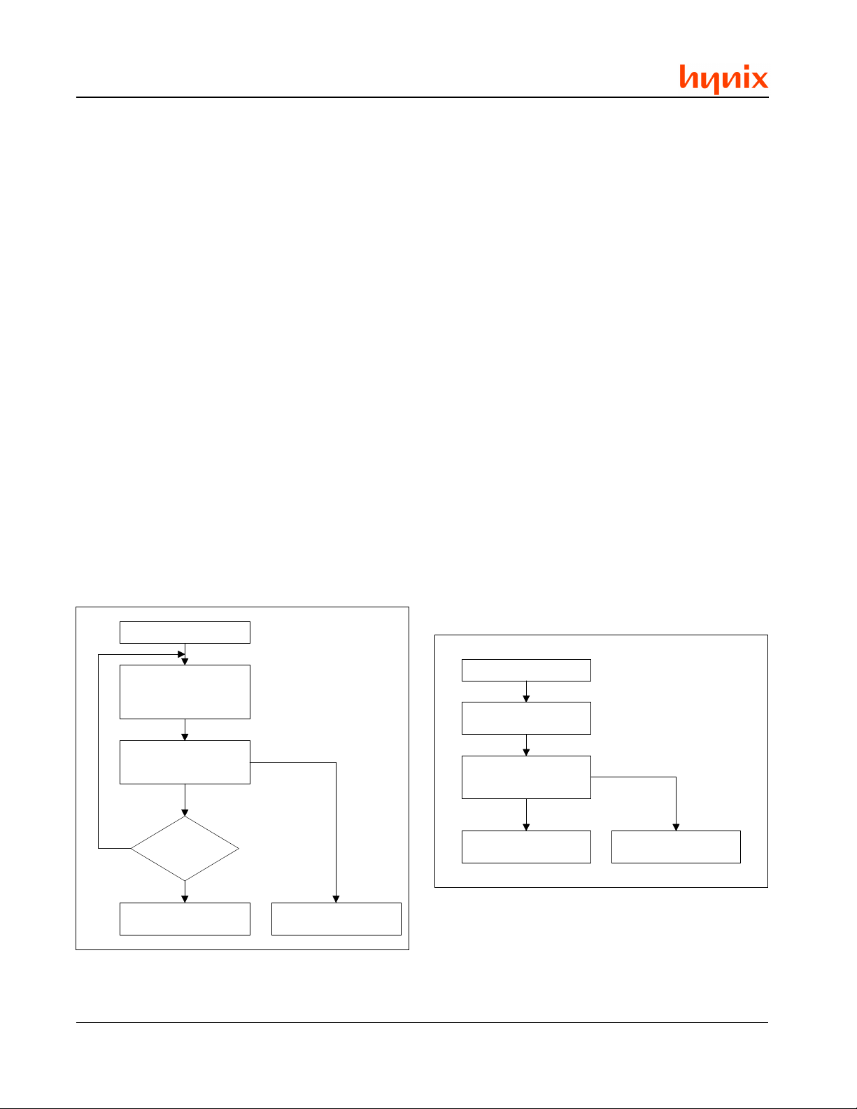
The flow chart in Figure 1 illustrates the procedure for protecting sector groups, and timing specifications and waveforms are shown in the specifications section of this document. Verification of
protection is accomplished as described in the
Electronic ID Mode section and shown in the flow
chart.
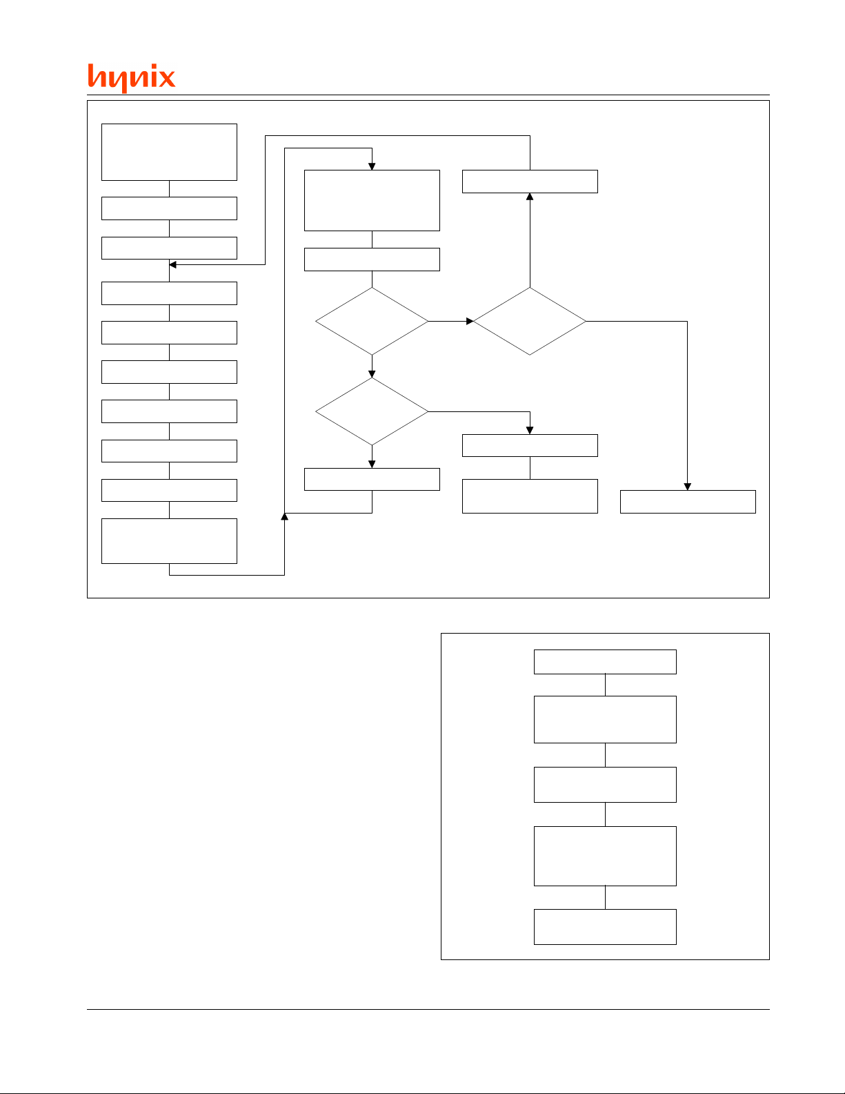
The procedure for sector group unprotection is illustrated in the flow chart in Figure 2, and timing
specifications and waveforms are given at the end
of this document. Note that to unprotect any sec-
tor group, all unprotected sector groups must first
be protected prior to the first unprotect write cycle.
Sectors can also be temporarily unprotected as
described in the next section.
Temporary Sector Group Unprotect Operation
This feature allows temporary unprotection of previously protected sectors to allow changing the
data in-system. Temporary Sector Group Unprotect mode is activated by setting the RESET# pin
to V
. While in this mode, formerly protected sec-
ID
tors can be programmed or erased by invoking
the appropriate commands (see Device Commands section). Once V
is removed from RE-
ID
SET#, all the previously protected sectors are protected again. Figure 3 illustrates the algorithm.
Electronic ID Mode Operation
The Electronic ID mode provides manufacturer and
device identification and sector group protection
verification through identifier codes output on
DQ[7:0]. This mode is intended primarily for programming equipment to automatically match a
device to be programmed with its corresponding
programming algorithm. The Electronic ID information can also be obtained by the host through
a command sequence, as described in the Device Commands section.
Operation in the Electronic ID mode requires V
on address pin A[9], with additional requirements
for obtaining specific data items as listed in Table
2:
n A read cycle at address 0xXXX00 retrieves the
manufacturer code (Hynix = 0xAD).
ID
START
APPLY V
Set TRYCNT = 1
Set A9 = OE# = V
Set Address:
A[19:17] = Group to Protect
RESET# = V
CE# = V
WE# = V
CC
ID
IL
IH
IL
Wait t
WPP1
WE# = V
IH
A9 = V
A[19:17] = Group to Protect
OE# = CE# = A6 = A0 = V
Data = 0x01?
Protect Another
ID
A1 = V
IH
Read Data
YES
Sector?
YES
IL
NO
NO
Increment TRYCNT
NO
TRYCNT = 25?
YES
DEVICE FAILURE
Figure 1. Sector Group Protect Procedure
Remove VID from A9
SECTOR PROTECT
COMPLETE
8
Rev. 6.1/May 01
Page 9
START
NOTE: All sectors must be
previously protected.
APPLY V
CC
Set Sector Group Address:
A[19:17] = Group NGRP
A0 = A6 = V
A1 = V
IL
IH
HY29F080
Increment TRYCNT
Set: TRYCNT = 1
Set: NGRP = 0
Set: A9 = CE# = OE# = V
Set: RESET# = V
WE# = V
Wait t
WPP2
WE# = V
Set:
A9 = V
OE# = CE# = V
ID
ID
IH
IL
IH
IL
Read Data
Data = 0x00?
YES
NGRP = 7?
NO
NGRP = NGRP + 1
Figure 2. Sector Group Unprotect Procedure
n A read cycle at address 0xXXX01 returns the
device code (HY29F080 = 0xD5).
n A read cycle containing a sector group address
(Table 1) in A[19:17] and the address 0x02 in
A[7:0] returns 0x01 if that sector is protected,
or 0x00 if it is unprotected.
NO
YES
NO
YES
TRYCNT = 1000?
Remove VID from A9
SECTOR UNPROTECT
COMPLETE
START
RESET# = V
(All protected sector groups
become unprotected)
DEVICE FAILURE
ID
Rev. 6.1/May 01
Perform Program or Erase
Operations
RESET# = V
(All previously protected
IH
sector groups return to
protected state)
TEMPORARY SECTOR
UNPROTECT COMPLETE
Figure 3. T emporary Sector Group Unprotect
9
Page 10
HY29F080
DEVICE COMMANDS
Device operations are initiated by writing designated address and data command sequences into
the device. A command sequence is composed
of one, two or three of the following sub-segments:
an unlock cycle, a command cycle and a data
cycle. Table 4 summarizes the composition of the
valid command sequences implemented in the
HY29F080, and these sequences are fully described in Table 5 and in the sections that follow.
Writing incorrect address and data values or writing them in the improper sequence resets the
HY29F080 to the Read mode.
Table 4. Composition of Command Sequences
dnammoC
ecneuqeS
1teseR/daeR011etoN
2teseR/daeR211etoN
margorPetyB211
esarEpihC411
esarErotceS41)2etoN(1
dnepsuSesarE010
emuseResarE010
DIcinortcelE213etoN
Notes:
1. Any number of Flash array read cycles are permitted.
2. Additional data cycles may follow. See text.
3. Any number of Electronic ID read cycles are permitted.
kcolnU dnammoC ataD
Read/Reset 1, 2 Commands
The HY29F080 automatically enters the Read
mode after device power-up, after the RESET#
input is asserted and upon the completion of certain commands. Read/Reset commands are not
required to retrieve data in these cases.
A Read/Reset command must be issued in order
to read array data in the following cases:
selcyCsuBforebmuN
Note: When in the Electronic ID bus operation mode,
the device returns to the Read mode when V
moved from the A[9] pin. The Read/Reset command is
not required in this case.
is re-
ID
n If DQ[5] (Exceeded T ime Limit) goes High dur-
ing a program or erase operation, writing the
reset command returns the sectors to the Read
mode (or to the Erase Suspend mode if the
device was in Erase Suspend).
The Read/Reset command may also be used to
abort certain command sequences:
n In a Sector Erase or Chip Erase command se-
quence, the Read/Reset command may be
written at any time before erasing actually begins, including, for the Sector Erase command,
between the cycles that specify the sectors to
be erased (see Sector Erase command description). This aborts the command and resets the device to the Read mode. Once erasure begins, however, the device ignores Read/
Reset commands until the operation is complete.
n In a Program command sequence, the Read/
Reset command may be written between the
sequence cycles before programming actually
begins. This aborts the command and resets
the device to the Read mode, or to the Erase
Suspend mode if the Program command sequence is written while the device is in the
Erase Suspend mode. Once programming
begins, however, the device ignores Read/Reset commands until the operation is complete.
n The Read/Reset command may be written be-
tween the cycles in an Electronic ID command
sequence to abort that command. As described
above, once in the Electronic ID mode, the
Read/ Reset command must be written to return to the Read mode.
Byte Program Command
n If the device is in the Electronic ID mode, a
Read/ Reset command must be written to return to the Read mode. If the device was in the
Erase Suspend mode when the device entered
the Electronic ID mode, writing the Read/Reset command returns the device to the Erase
Suspend mode.
10
The host processor programs the device a byte at
a time by issuing the Program command sequence
shown in Table 5. The sequence begins by writing two unlock cycles, followed by the Program
setup command and, lastly, a data cycle specifying the program address and data. This initiates
the Automatic Programming algorithm, which provides internally generated program pulses and
Rev. 6.1/May 01
Page 11
HY29F080
3,2,1
selcyCsuB
00XDA
tsriF dnoceS drihT htruoF htfiF htxiS
ddA ataD ddA ataD ddA ataD ddA ataD ddA ataD ddA ataD
selcyC
etirW
1XXX0FARDR
3555AAAA2555550FARDR
1XXX0B
1XXX03
3555AAAA25555509
edoCrerutcafunaM
ecneuqeSdnammoC
edoCeciveD 10X5D
8,7
8,6
2teseR/teseR
1teseR/daeR
margorPetyB4555AAAA2555550AAPDP
4
5
dnepsuSesarE
esarErotceS6555AAAA25555508555AAAA255AS03
esarEpihC6555AAAA25555508555AAAA25555501
emuseResarE
cinortcelE
7
Table 5. HY29F080 Command Sequences
Rev. 6.1/May 01
DI
yfireVtcetorPpuorG AVPGTATS
• For RA and PA, A[19:11] are the upper address bits of the byte to be read or programmed.
• For SA, A[19:16] are the sector address of the sector to be erased and A[15:0] are don’t care.
• For GPVA, A[19:17] are the sector group address of the sector to be verified, A[7:0] = 0x02, all other address bits are don’t care.
Legend:
X = Don’t Care PA = Address of the data to be programmed
RA = Memory address of data to be read PD = Data to be programmed at address PA
RD = Data read from location RA during the read operation SA = Sector address of sector to be erased (see Note 3 and Table 1).
STAT = Group protect status: 0x00 = unprotected, 0x01 = protected. GPVA = Address of the sector group to be verified (see Note 3 and Table 1).
Notes:
1. All values are in hexadecimal.
2. All bus cycles are write operations unless otherwise noted.
3. Address is A[10:0] and A[19:11] are don’t care except as follows:
Electronic ID mode, while in the Erase Suspend mode.
4. The Erase Suspend command is valid only during a sector erase operation. The system may read and program in non-erasing sectors, or enter the
5. The Erase Resume command is valid only during the Erase Suspend mode.
6. The second bus cycle is a read cycle.
DQ[5] goes High during a program or erase operation. It is not required for normal read operations.
7. The fourth bus cycle is a read cycle.
8. Either command sequence is valid. The command is required only to return to the Read mode when the device is in the Electronic ID command mode or if
11
Page 12
HY29F080
verifies the programmed cell margin. The host is
not required to provide further controls or timings
during this operation. When the Automatic Programming algorithm is complete, the device returns to the Read mode. Several methods are
provided to allow the host to determine the status
of the programming operation, as described in the
Write Operation Status section.
Commands written to the device during execution
of the Automatic Programming algorithm are ignored. Note that a hardware reset immediately
terminates the programming operation. To ensure data integrity, the aborted program command
sequence should be reinitiated once the reset
operation is complete.
Programming is allowed in any sequence. Only
erase operations can convert a stored “0” to a “1”.
Thus, a bit cannot be programmed from a “0” back
to a “1”. Attempting to do so will set DQ[5] to “1”,
and the Data# Polling algorithm will indicate that
the operation was not successful. A Read/Reset
command or a hardware reset is required to exit
this state, and a succeeding read will show that
the data is still “0”.
Figure 4 illustrates the procedure for the Program
operation.
Chip Erase Command
The Chip Erase command sequence consists of
two unlock cycles, followed by the erase command, two additional unlock cycles and then the
chip erase data cycle. During chip erase, all sectors of the device are erased except protected
sector groups. The command sequence starts the
Automatic Erase algorithm, which preprograms
and verifies the entire memory, except for protected sector groups, for an all zero data pattern
prior to electrical erase. The device then provides
the required number of internally generated erase
pulses and verifies cell erasure within the proper
cell margins. The host system is not required to
provide any controls or timings during these operations.
Commands written to the device during execution
of the Automatic Erase algorithm are ignored. Note
that a hardware reset immediately terminates the
erase operation. To ensure data integrity, the
aborted chip erase command sequence should be
reissued once the reset operation is complete.
When the Automatic Erase algorithm is finished,
the device returns to the Read mode. Several
methods are provided to allow the host to determine the status of the erase operation, as described in the Write Operation Status section.
START
Issue PROGRAM
Command Sequence:
Last cycle contains
program Address/Data
Check Programming Status
(See Write Operation Status
NO
Section)
Normal Exit
Last Byte Done?
YES
PROGRAMMING
COMPLETE
DQ[5] Error Exit
GO TO
ERROR RECOVERY
Figure 4. Programming Procedure
Figure 5 illustrates the Chip Erase procedure.
START
Issue CHIP ERASE
Command Sequence
Check Erase Status
(See Write Operation Status
Section)
Normal Exit
CHIP ERASE COMPLETE
DQ[5] Error Exit
GO TO
ERROR RECOVERY
Figure 5. Chip Erase Procedure
Sector Erase Command
The Sector Erase command sequence consists
of two unlock cycles, followed by the erase command, two additional unlock cycles and then the
sector erase data cycle, which specifies which
12
Rev. 6.1/May 01
Page 13

HY29F080
sector is to be erased. As described later in this
section, multiple sectors can be specified for erasure with a single command sequence. During
sector erase, all specified sectors are erased sequentially. The data in sectors not specified for
erasure, as well as the data in any sectors specified for erasure but located within protected sector groups, is not affected by the sector erase operation.
The Sector Erase command sequence starts the
Automatic Erase algorithm, which preprograms
and verifies the specified unprotected sectors for
an all zero data pattern prior to electrical erase.
The device then provides the required number of
internally generated erase pulses and verifies cell
erasure within the proper cell margins. The host
system is not required to provide any controls or
timings during these operations.
After the sector erase data cycle (the sixth bus
cycle) of the command sequence is issued, a sector erase time-out of 50 µs (typical), measured from
the rising edge of the final WE# pulse in that bus
cycle, begins. During this time, an additional sector erase data cycle, specifying the sector address
of another sector to be erased, may be written
into an internal sector erase buffer. This buffer
may be loaded in any sequence, and the number
of sectors specified may be from one sector to all
sectors. The only restriction is that the time between these additional data cycles must be less
than 50 µs, otherwise erasure may begin before
the last data cycle is accepted. To ensure that all
data cycles are accepted, it is recommended that
host processor interrupts be disabled during the
time that the additional cycles are being issued
and then be re-enabled afterwards.
Note: The device is capable of accepting three ways
of invoking Erase Commands for additional sectors
during the time-out window. The preferred method,
described above, is the sector erase data cycle after
the initial six bus cycle command sequence. However, the device also accepts the following methods
of specifying additional sectors during the sector
erase time-out:
n Repeat the entire six-cycle command sequence, speci-
fying the additional sector in the sixth cycle.
n Repeat the last three cycles of the six-cycle command
sequence, specifying the additional sector in the third
cycle.
If all sectors scheduled for erasing are within protected sector groups, the device returns to reading array data after approximately 100 µs. If at
least one selected sector is not protected, the
erase operation erases the unprotected sectors,
and ignores the command for the selected sectors that are protected.
The system can monitor DQ[3] to determine if the
50 µs sector erase time-out has expired, as described in the Write Operation Status section. If
the time between additional sector erase data
cycles can be insured to be less than the timeout, the system need not monitor DQ[3].
Any command other than Sector Erase or Erase
Suspend during the time-out period resets the
device to reading array data. The system must
then rewrite the command sequence, including any
additional sector erase data cycles. Once the
sector erase operation itself has begun, only the
Erase Suspend command is valid. All other commands are ignored.
As for the Chip Erase command, note that a hardware reset immediately terminates the erase operation. To ensure data integrity, the aborted Sector Erase command sequence should be reissued
once the reset operation is complete.
When the Automatic Erase algorithm terminates,
the device returns to the Read mode. Several
methods are provided to allow the host to determine the status of the erase operation, as described in the Write Operation Status section.
Figure 6 illustrates the Sector Erase procedure.
Erase Suspend/Erase Resume Commands
The Erase Suspend command allows the system
to interrupt a sector erase operation to read data
from, or program data in, any sector not being
erased. The command causes the erase operation to be suspended in all sectors selected for
erasure. This command is valid only during the
sector erase operation, including during the 50 µs
time-out period at the end of the initial command
sequence and any subsequent sector erase data
cycles, and is ignored if it is issued during chip
erase or programming operations.
The HY29F080 requires a maximum of 15 µs to
suspend the erase operation if the Erase Suspend
command is issued during active sector erasure.
However, if the command is written during the timeout, the time-out is terminated and the erase operation is suspended immediately. Any subsequent attempts to specify additional sectors for
Rev. 6.1/May 01
13
Page 14

HY29F080
START
Write First Five Cycles of
SECTOR ERASE
Command Sequence
Setup First (or Next) Sector
Address for Erase Operation
Check Erase Status
(See Write Operation Status
Section)
Normal Exit
ERASE COMPLETE
DQ[5] Error Exit
GO TO
ERROR RECOVERY
Write Last Cycle (SA/0x30)
of SECTOR ERASE
Command Sequence
NO
Erase An
Additional Sector?
NO
YES
Sector Erase
Time-out (DQ[3])
Expired?
YES
Figure 6. Sector Erase Procedure
erasure by writing the sector erase data cycle (SA/
0x30) will be interpreted as the Erase Resume
command (XXX/0x30), which will cause the Automatic Erase algorithm to begin its operation. Note
that any other command during the time-out will
reset the device to the Read mode.
Once the erase operation has been suspended,
the system can read array data from or program
data to any sector not selected for erasure. Normal read and write timings and command definitions apply. Reading at any address within erasesuspended sectors produces status data on
DQ[7:0]. The host can use DQ[7], or DQ[6] and
DQ[2] together, to determine if a sector is actively
erasing or is erase-suspended. See “Write Operation Status” for information on these status bits.
After an erase-suspended program operation is
complete, the host can initiate another programming operation (or read operation) within non-suspended sectors. The host can determine the status of a program operation during the erase-suspended state just as in the standard programming
operation.
The system must write the Erase Resume command to exit the Erase Suspend mode and continue the sector erase operation. Further writes of
Sectors which require erasure
but which were not specified in
this erase cycle must be erased
later using a new command
sequence
the Resume command are ignored. Another Erase
Suspend command can be written after the device has resumed erasing.
The host may also write the Electronic ID command sequence when the device is in the Erase
Suspend mode. The device allows reading Electronic ID codes even if the addresses used for the
ID read cycles are within erasing sectors, since
the codes are not stored in the memory array.
When the device exits the Electronic ID mode, the
device reverts to the Erase Suspend mode, and
is ready for another valid operation. See Electronic
ID section for more information.
Electronic ID Command
The Electronic ID operation intended for use in
programming equipment has been described previously. The host processor can also be obtain
the same data by using the Electronic ID command sequence shown in Table 5. This method
does not require V
on any pin. The Electronic ID
ID
command sequence may be invoked while the
device is in the Read mode or the Erase Suspend
mode, but is invalid while the device is actively
programming or erasing.
14
Rev. 6.1/May 01
Page 15

HY29F080
The Electronic ID command sequence is initiated
by writing two unlock cycles, followed by the Electronic ID command. The device then enters the
Electronic ID mode, and:
n A read cycle at address 0xXXX00 retrieves the
manufacturer code (Hynix = 0xAD).
n A read cycle at address 0xXXX01 returns the
device code (29F080 = 0xD5).
mand sequence. Thus, for example, the host may
determine the protection status for all sector
groups by doing successive reads at address 0x02
while changing the SGA in A[19:17] for each cycle.
The system must write the Reset command to exit
the Electronic ID mode and return to the Read
mode, or to the Erase Suspend mode if the device was in that mode when the command sequence was issued.
n A read cycle containing a sector group address
(SGA) in A[19:17] and the address 0x02 in
A[7:0] returns 0x01 if that sector is protected,
or 0x00 if it is unprotected.
The host system may read at any address any
number of times, without initiating another com-
WRITE OPERATION STATUS
The HY29F080 provides a number of facilities to
determine the status of a program or erase operation. These are the RY/BY# (Ready/Busy#)
pin and certain bits of a status word which can be
read from the device during the programming and
erase operations. Table 6 summarizes the status
indications and further detail is provided in the
subsections which follow.
Table 6. Write and Erase Operation Status Summary
edoM noitarepO ]7[QD
ssergorpnignimmargorP#]7[QDelggoT1/0
lamroN
detelpmocgnimmargorPataDataD
ssergorpniesarE0elggoT1/0
detelpmocesarE1ataD
dednepsusesarenihtiwdaeR
rotces
esarE
dnepsuS
Notes:
1. A valid address is required when reading status information. See text for additional information.
2. DQ[5] status switches to a ‘1’ when a program or erase operation exceeds the maximum timing limit.
3. A ‘1’ during sector erase indicates that the 50 µs timeout has expired and active erasure is in progress. DQ[3] is not
applicable to the chip erase operation.
4. Equivalent to ‘No Toggle’ because data is obtained in this state.
5. Programming can be done only in a non-suspended sector (a sector not marked for erasure).
esare-nonnihtiwdaeR
rotcesdednepsus
5
ssergorpnignimmargorP
5
detelpmocgnimmargorP
1
]6[QD ]5[QD ]3[QD ]2[QD
2
4
4
ataDataDataD1
2
ataDataDataD
A/NA/N0
3
1
1elggotoN0A/NelggoT1
ataDataDataDataDataD1
#]7[QDelggoT1/0
ataDataD
4
2
A/NA/N0
ataDataDataD1
1
#YB/YR
elggoT0
4
1
RY/BY# - Ready/Busy#
RY/BY# is an open-drain output pin that indicates
whether a programming or erase Automatic Algorithm is in progress or has completed. A pull-up
resistor to V
is required for proper operation. RY/
CC
BY# is valid after the rising edge of the final WE#
pulse in the corresponding command sequence.
Rev. 6.1/May 01
If the output is Low (busy), the device is actively
erasing or programming, including programming
while in the Erase Suspend mode. If the output is
High (ready), the device has completed the operation and is ready to read array data in the normal or Erase Suspend modes, or it is in the standby
mode.
15
Page 16

HY29F080
DQ[7] - Data# Polling
The Data# (“Data Bar”) Polling bit, DQ[7], indicates
to the host system whether an Automatic Algorithm is in progress or completed, or whether the
device is in Erase Suspend mode. Data# Polling
is valid after the rising edge of the final WE# pulse
in the Program or Erase command sequence.
The system must do a read at the program address to obtain valid programming status information on this bit. While a programming operation is
in progress, the device outputs the complement
of the value programmed to DQ[7]. When the programming operation is complete, the device outputs the value programmed to DQ[7]. If a program operation is attempted within a protected
sector, Data# Polling on DQ[7] is active for approximately 2 µs, then the device returns to reading array data.
The host must read at an address within any nonprotected sector scheduled for erasure to obtain
valid erase status information on DQ[7]. During
an erase operation, Data# Polling produces a “0”
on DQ[7]. When the erase operation is complete,
or if the device enters the Erase Suspend mode,
Data# Polling produces a “1” on DQ[7]. If all sectors selected for erasing are protected, Data#
Polling on DQ[7] is active for approximately 100
µs, then the device returns to reading array data.
If at least one selected sector is not protected, the
erase operation erases the unprotected sectors,
and ignores the command for the selected sectors that are protected.
START
Read DQ[7:0]
at Valid Address (Note 1)
Test for DQ[7] = 1?
for Erase Operation
DQ[7] = Data?
NO
NO
Notes:
1. During programming, the program address.
During sector erase, an address within any non-protected sector
scheduled for erasure.
During chip erase, an address within any non-protected sector.
2. Recheck DQ[7] since it may change asynchronously at the same time
as DQ[5].
DQ[5] = 1?
YES
Read DQ[7:0]
at Valid Address (Note 1)
DQ[7] = Data?
(Note 2)
NO
PROGRAM/ERASE
EXCEEDED TIME ERROR
YES
Test for DQ[7] = 1?
for Erase Operation
YES
PROGRAM/ERASE
COMPLETE
Figure 7. Data# Polling Test Algorithm
When the system detects that DQ[7] has changed
from the complement to true data (or “0” to “1” for
erase), it should do an additional read cycle to read
valid data from DQ[7:0]. This is because DQ[7]
may change asynchronously with respect to the
other data bits while Output Enable (OE#) is asserted low.
Figure 7 illustrates the Data# Polling test algorithm.
DQ[6] - Toggle Bit I
Toggle Bit I on DQ[6] indicates whether an Automatic Program or Erase algorithm is in progress
or complete, or whether the device has entered
the Erase Suspend mode. Toggle Bit I may be
read at any address, and is valid after the rising
edge of the final WE# pulse in the program or erase
command sequence, including during the sector
16
erase time-out. The system may use either OE#
or CE# to control the read cycles.
Successive read cycles at any address during an
Automatic Program algorithm operation (including
programming while in Erase Suspend mode)
cause DQ[6] to toggle. DQ[6] stops toggling when
the operation is complete. If a program address
falls within a protected sector, DQ[6] toggles for
approximately 2 µs after the program command
sequence is written, then returns to reading array
data.
While the Automatic Erase algorithm is operating,
successive read cycles at any address cause
DQ[6] to toggle. DQ[6] stops toggling when the
erase operation is complete or when the device is
placed in the Erase Suspend mode. The host may
use DQ[2] to determine which sectors are erasing
Rev. 6.1/May 01
Page 17

START
HY29F080
Read DQ[7:0]
at Valid Address (Note 1)
Read DQ[7:0]
at Valid Address (Note 1)
DQ[6] Toggled?
NO
(Note 4)
NO
(Note 3)
PROGRAM/ERASE
COMPLETE
:
Notes
1. During programming, the program address.
During sector erase, an address within any sector scheduled for erasure.
2. Recheck DQ[6] since toggling may stop at the same time as DQ[5] changes from 0 to 1.
3. Use this path if testing for Program/Erase status.
4. Use this path to test whether sector is in Erase Suspend mode.
YES
NO
NO
DQ[5] = 1?
YES
Read DQ[7:0]
at Valid Address (Note 1)
DQ[6] Toggled?
(Note 2)
YES
PROGRAM/ERASE
EXCEEDED TIME ERROR
Read DQ[7:0]
Read DQ[7:0]
DQ[2] Toggled?
SECTOR BEING READ
IS IN ERASE SUSPEND
Figure 8. Toggle Bit I and II Test Algorithm
or erase-suspended (see below). After an Erase
command sequence is written, if all sectors selected for erasing are protected, DQ[6] toggles for
approximately 100 µs, then returns to reading array data. If at least one selected sector is not
protected, the Automatic Erase algorithm erases
the unprotected sectors, and ignores the selected
sectors that are protected.
Thus, both status bits are required for sector and
mode information.
Figure 8 illustrates the operation of Toggle Bits I
and II.
DQ[5] - Exceeded Timing Limits
DQ[5] is set to a ‘1’ when the program or erase
time has exceeded a specified internal pulse count
DQ[2] - Toggle Bit II
Toggle Bit II, DQ[2], when used with DQ[6], indicates whether a particular sector is actively erasing or whether that sector is erase-suspended.
Toggle Bit II is valid after the rising edge of the
final WE# pulse in the command sequence. The
device toggles DQ[2] with each OE# or CE# read
cycle.
DQ[2] toggles when the host reads at addresses
within sectors that have been selected for erasure,
but cannot distinguish whether the sector is actively erasing or is erase-suspended. DQ[6], by
limit. This is a failure condition that indicates that
the program or erase cycle was not successfully
completed. DQ[5] status is valid only while DQ[7]
or DQ[6] indicate that an Automatic Algorithm is
in progress.
The DQ[5] failure condition will also be signaled if
the host tries to program a ‘1’ to a location that is
previously programmed to ‘0’, since only an erase
operation can change a ‘0’ to a ‘1’.
For both of these conditions, the host must issue
a Read/Reset command to return the device to
the Read mode.
comparison, indicates whether the device is actively erasing or is in Erase Suspend, but cannot
distinguish which sectors are selected for erasure.
NO
YES
SECTOR BEING READ
IS NOT IN ERASE SUSPEND
Rev. 6.1/May 01
17
Page 18

HY29F080
DQ[3] - Sector Erase Timer
After writing a Sector Erase command sequence,
the host may read DQ[3] to determine whether or
not an erase operation has begun. When the
sector erase time-out expires and the sector erase
operation commences, DQ[3] switches from a ‘0’
to a ‘1’. Refer to the “Sector Erase Command”
section for additional information. Note that the
sector erase timer does not apply to the Chip Erase
command.
After the initial Sector Erase command sequence
is issued, the system should read the status on
HARDWARE DATA PROTECTION
The HY29F080 provides several methods of protection to prevent accidental erasure or programming which might otherwise be caused by spurious system level signals during V
power-up and
CC
power-down transitions, or from system noise.
These methods are described in the sections that
follow.
Command Sequences
Commands that may alter array data require a
sequence of cycles as described in Table 5. This
provides data protection against inadvertent writes.
Low V
To protect data during V
Write Inhibit
CC
power-up and power-
CC
down, the device does not accept write cycles
when V
is less than V
CC
(typically 3.7 volts). The
LKO
command register and all internal program/erase
circuits are disabled, and the device resets to the
Read mode. Writes are ignored until V
than V
. The system must provide the proper
LKO
is greater
CC
signals to the control pins to prevent unintentional
writes when V
is greater than V
CC
LKO
.
DQ[7] (Data# Polling) or DQ[6] (Toggle Bit I) to
ensure that the device has accepted the command
sequence, and then read DQ[3]. If DQ[3] is a ‘1’,
the internally controlled erase cycle has begun and
all further sector erase data cycles or commands
(other than Erase Suspend) are ignored until the
erase operation is complete. If DQ[3] is a ‘0’, the
device will accept a sector erase data cycle to mark
an additional sector for erasure. To ensure that
the data cycles have been accepted, the system
software should check the status of DQ[3] prior to
and following each subsequent sector erase data
cycle. If DQ[3] is high on the second status check,
the last data cycle might not have been accepted.
Write Pulse “Glitch” Protection
Noise pulses of less than 5 ns (typical) on OE#,
CE# or WE# do not initiate a write cycle.
Logical Inhibit
Write cycles are inhibited by asserting any one of
the following conditions: OE# = V
WE# = V
. To initiate a write cycle, CE# and WE#
IH
, CE# = VIH, or
IL
must be a logical zero while OE# is a logical one.
Power-Up Write Inhibit
If WE# = CE# = V
and OE# = VIH during power
IL
up, the device does not accept commands on the
rising edge of WE#. The internal state machine is
automatically reset to the Read mode on powerup.
Sector Group Protection
Additional data protection is provided by the
HY29F080’s sector group protect feature, described previously, which can be used to protect
sensitive areas of the Flash array from accidental
or unauthorized attempts to alter the data.
18
Rev. 6.1/May 01
Page 19

HY29F080
ABSOLUTE MAXIMUM RATINGS
4
lobmyS retemaraP eulaV tinU
T
GTS
T
SAIB
V
2NI
I
SO
CCV
Notes:
1. Minimum DC voltage on input or I/O pins is –0.5 V. During voltage transitions, input or I/O pins may undershoot V
-2.0V for periods of up to 20 ns. See Figure 9. Maximum DC voltage on input or I/O pins is V
transitions, input or I/O pins may overshoot to V
2. Minimum DC input voltage on pins A[9], OE#, and RESET# is -0.5 V. During voltage transitions, A[9], OE#, and RESET#
may undershoot V
V which may overshoot to 13.5 V for periods up to 20 ns.
to –2.0 V for periods of up to 20 ns. See Figure 9. Maximum DC input voltage on these pins is +12.5
SS
3. No more than one output at a time may be shorted to V
4. Stresses above those listed under “Absolute Maximum Ratings” may cause permanent damage to the device. This is a
stress rating only; functional operation of the device at these or any other conditions above those indicated in the
operational sections of this data sheet is not implied. Exposure of the device to absolute maximum rating conditions for
extended periods may affect device reliability.
RECOMMENDED OPERATING CONDITIONS
erutarepmeTegarotS 521+ot56-Cº
deilppArewoPhtiwerutarepmeTtneibmA 521+ot55-Cº
VottcepseRhtiwniPnoegatloV
:
1
1
sniPrehtOllA
SS
2
#TESER,#EO,]9[A
3
tnerruCtiucriCtrohStuptuO
+2.0 V for periods up to 20 ns. See Figure 10.
CC
. Duration of the short circuit should be less than one second.
SS
1
002Am
CC
0.7+ot0.2-
5.31+ot0.2-
0.7+ot0.2-
+ 0.5 V. During voltage
V
V
V
to
SS
lobmyS retemaraP eulaV tinU
T
A
V
CC
Notes:
1. Recommended Operating Conditions define those limits between which the functionality of the device is guaranteed.
erutarepmeTgnitarepOtneibmA07+ot0Cº
egatloVylppuSgnitarepO 05.5+ot05.4+V
20 ns
0.8 V
20 ns 20 ns
VCC + 2.0 V
- 0.5 V
V
+ 0.5 V
CC
- 2.0 V
20 ns
2.0 V
20 ns 20 ns
Figure 9. Maximum Undershoot Waveform Figure 10. Maximum Overshoot Waveform
Rev. 6.1/May 01
19
Page 20

HY29F080
DC CHARACTERISTICS
TTL/NMOS Compatible
retemaraP noitpircseD puteStseT niM pyT xaM tinU
V
V=
Vot
NI
I
IL
I
TIL
I
OL
I
I
I
I
V
LI
V
HI
V
DI
V
V
V
V
1CC
2CC
3CC
4CC
LO
HO
OKL
CC
V
CC
V
CC
V
CC
VwoL
CC
tnerruCdaoLtupnI
tnerruCdaoLtupnI]9[A
tnerruCegakaeLtuptuO
1
tnerruCdaeRevitcA
tnerruCetirWevitcA
dellortnoC#EC
V
V
V
V
3,2
VCCV=
tnerruCybdnatSLTT
dellortnoC#TESER
VCCV=
tnerruCybdnatSLTT
egatloVwoLtupnI5.0-8.0V
egatloVhgiHtupnI0.2V
dnaDIcinortcelErofegatloV
V
tcetorpnUrotceSyraropmeT
egatloVwoLtuptuO
egatloVhgiHtuptuO
3
egatloVtuokcoL
V
I
V
I
SS
V=
CC
CC
V=
CC
CC
V=
TUO
V=
CC
CC
V=#EC
V=#EC
CC
CC
CC
V=
CC
CC
LO
V=
CC
CC
HO
Notes:
1. Includes both the DC Operating Current and the frequency dependent component at 6 MHz. The read component of the
I
current is typically less than 1 ma/MHz with OE# at VIL.
CC
2. I
active while Automatic Erase or Automatic Program algorithm is in progress.
CC
3. Not 100% tested.
,
CC
xaM
,xaM
V5.21=]9[A
Vot
SS
,
CC
xaM
LI
LI
V=#EO,
HI
V=#EO,
HI
,xaM
V=#TESER=#EC
HI
,xaM
V=#TESER
LI
5204Am
0406Am
4.00.1Am
4.00.1Am
0.1±Aµ
05Aµ
0.1±Aµ
5.0+V
CC
V0.5=5.115.21V
,niM
am0.21=
,niM
Am5.2-=
4.2V
54.0V
2.32.4V
20
Rev. 6.1/May 01
Page 21

HY29F080
DC CHARACTERISTICS
CMOS Compatible
retemaraP noitpircseD puteStseT niM pyT xaM tinU
I
IL
I
TIL
I
OL
I
I
I
I
V
LI
V
HI
V
DI
V
V
V
V
1CC
2CC
3CC
4CC
LO
HO
OKL
CC
V
CC
V
CC
V
CC
VwoL
CC
tnerruCdaoLtupnI
tnerruCdaoLtupnI]9[A
tnerruCegakaeLtuptuO
1
tnerruCdaeRevitcA
tnerruCetirWevitcA
dellortnoC#EC
tnerruCybdnatSSOMC
dellortnoC#TESER
tnerruCybdnatSSOMC
egatloVwoLtupnI5.0-8.0V
egatloVhgiHtupnIVx7.0
egatloVwoLtuptuO
egatloVhgiHtuptuO
3
egatloVtuokcoL
VNIV=
V
CC
V
CC
V
TUO
V
CC
3,2
V
CC
V
CC
dnaDIcinortcelErofegatloV
V
tcetorpnUrotceSyraropmeT
CC
V
CC
I
LO
V
CC
I
HO
V
CC
I
HO
Notes:
1. Includes both the DC Operating Current and the frequency dependent component at 6 MHz. The read component of the
I
current is typically less than 1 ma/MHz with OE# at VIL.
CC
2. ICC active while Automatic Erase or Automatic Program algorithm is in progress.
3. Not 100% tested.
Vot
SS
V=
CC
V=
CC
V=
V=
CC
V=#EC
V=#EC
V=
V=
CC
,
CC
xaM
,xaM
V5.21=]9[A
Vot
SS
,
CC
xaM
LI
LI
CC
V=#EO,
HI
V=#EO,
HI
=#EC,xaM
V=#TESER
± V5.0
CC
,xaM
V=#TESER
± V5.0
SS
CC
5204Am
0304Am
15Aµ
15Aµ
V
CC
0.1±Aµ
05Aµ
0.1±Aµ
3.0+V
V0.5=5.115.21V
V=
V=
V=
CC
CC
CC
001-=Aµ
,niM
am0.21=
,niM
Am5.2-=
,niM
x58.0
V
CC
V
4.0-V
CC
54.0V
V
2.32.4V
KEY TO SWITCHING WAVEFORMS
MROFEVAW STUPNI STUPTUO
Rev. 6.1/May 01
ydaetS
LotHmorfgnignahC
HotLmorfgnignahC
dettimrePegnahCynA,eraCt'noDnwonknUetatS,gnignahC
ylppAtoNseoD
)ZhgiH(
etatSecnadepmIhgiHsienilretneC
21
Page 22

HY29F080
TEST CONDITIONS
DEVICE
UNDER
TEST
2.4 V
0.45 V
+ 5V
C
L
6.2
KOhm
Figure 11. Test Setup
2.7
KOhm
All diodes
are
1N3064
or
equivalent
2.0 V
0.8 V
Table 7. Test Specifications
tseT
noitidnoC
daoLtuptuOetaGLTT1
leveLlangiS
leveLlangiS
2.0 V
Measurement
Levels
0.8 V
0709-
tinU
21-
C(ecnaticapaCdaoLtuptuO
)001Fp
L
semiTllaFdnaesiRtupnI02sn
leveLwoLlangiStupnI54.0V
leveLhgiHlangiStupnI4.2V
tnemerusaeMgnimiTwoL
tnemerusaeMgnimiThgiH
8.0V
0.2V
OutputInput
HY29F080-70, -90, -12 Versions
Figure 12. Input Waveforms and Measurement Levels
22
Rev. 6.1/May 01
Page 23

AC CHARACTERISTICS
Read Operations
retemaraP
CEDEJ dtS 07- 09- 21-
t
t
t
t
t
t
t
Notes:
1. Not 100% tested.
2. See Figure 11 and Table 7 for test conditions.
t
VAVA
VQVA
VQLE
ZQHE
VQLG
ZQHG
XQXA
CR
t
CCA
t
EC
t
FD
t
EO
t
FD
t
HEO
t
HO
elbanEtuptuO
yaleDtuptuOotsserddA
)1etoN(emiTdloH
HY29F080
noitpircseD puteStseT
)1etoN(emiTelcyCdaeRniM0709021sn
V=#EC
yaleDtuptuOotelbanEpihCV=#EO
LI
V=#EO
LI
LI
xaM0709021sn
xaM0709021sn
)1etoN(ZhgiHtuptuOotelbanEpihCxaM020203sn
yaleDtuptuOotelbanEtuptuOV=#EC
LI
xaM035305sn
)1etoN(ZhgiHtuptuOotelbanEtuptuOxaM020203sn
daeRniM0sn
dnaelggoT
gnilloP#ataD
#EC,sesserddAmorfemiTdloHtuptuO
)1etoN(tsriFsruccOrevehcihW,#EOro
niM01sn
niM0sn
noitpOdeepS
tinU
Addresses
CE#
OE#
WE#
Outputs
RESET#
t
OEH
t
RC
Addresses Stable
t
ACC
t
OE
t
CE
t
OH
Output Valid
t
DF
RY/BY#
Rev. 6.1/May 01
0 V
Figure 13. Read Operation Timings
23
Page 24

HY29F080
AC CHARACTERISTICS
Hardware Reset (RESET#)
retemaraP
CEDEJ dtS 07- 09- 21-
t
YDAER
)1
t
YDAER
t
PR
t
HR
Notes:
1. Not 100% tested.
2. See Figure 11 and Table 7 for test conditions.
)1etoNees(
htdiWesluP#TESERniM005sn
)1etoN
noitpircseD puteStseT
citamotuAgniruD(woLniP#TESER
etoNees(etirWrodaeRot)smhtiroglA
gniruDTON(woLniP#TESER
etirWrodaeRot)smhtiroglAcitamotuA
ees(daeRerofeBemiThgiH#TESER
noitpOdeepS
xaM02sµ
xaM005sn
niM05sn
tinU
RY/BY#
CE#, OE#
RESET#
RY/BY#
CE#, OE#
RESET#
0 V
t
RH
t
RP
t
READY
Reset Timings NOT During Automatic Algorithms
Reset Timings NOT During Automatic Algorithms
t
READY
t
RP
Reset Timings During Automatic Algorithms
Reset Timings During Automatic Algorithms
t
RH
24
Figure 14. RESET# Timings
Rev. 6.1/May 01
Page 25

AC CHARACTERISTICS
Program and Erase Operations
HY29F080
retemaraP
CEDEJ dtS 07- 09- 21-
t
t
t
t
t
t
t
t
t
t
t
t
t
t
VAVA
LWVA
XALW
HWVD
XDHW
LWHG
LWLE
HEHW
HWLW
LWHW
1HWHW
2HWHW
3HWHW
CW
t
SA
t
HA
t
SD
t
HD
t
LWHG
t
SC
t
HC
t
PW
t
HPW
t
1HWHW
t
2HWHW
t
3HWHW
V
t
SCV
CC
t
BR
t
YSUB
emiTputeSsserddAniM0sn
emiTdloHsserddAniM545405sn
emiTputeSataDniM035405sn
emiTdloHataDniM0sn
emiTputeS#ECniM0sn
emiTdloH#ECniM0sn
htdiWesluPetirWniM535405sn
hgiHhtdiWesluPetirWniM02sn
emiTputeSniM05sµ
yaleD#YB/YRot#EWniM040405sn
noitpircseD
)1etoN(emiTelcyCetirWniM0709021sn
etirWerofeBemiTyrevoceRdaeRniM0sn
)3,2,1setoN(noitarepOgnimmargorPetyB
)5,3,2,1setoN(noitarepOgnimmargorPpihC
)4,2,1setoN(noitarepOesarErotceS
)4,2,1setoN(noitarepOesarEpihC
ecnarudnEelcyCmargorPdnaesarE
pyT7sµ
xaM003sµ
pyT2.7ces
xaM6.12ces
pyT1ces
xaM8ces
pyT61ces
xaM821ces
pyT000,000,1selcyc
niM000,001selcyc
#YB/YRmorfemiTyrevoceRniM0sn
noitpOdeepS
tinU
Notes:
1. Not 100% tested.
2. Typical program and erase times assume the following conditions: 25 °C, V
programming typicals assume a checkerboard pattern. Maximum program and erase times are under worst case conditions of 90 °C, V
3. Excludes system-level overhead, which is the time required to execute the four-bus-cycle sequence for the program
= 4.5 volts, 100,000 cycles.
CC
= 5.0 volts, 100,000 cycles. In addition,
CC
command. See Table 5 for further information on command sequences.
4. Excludes 0x00 programming prior to erasure. In the preprogramming step of the Automatic Erase algorithm, all bytes
are programmed to 0x00 before erasure.
5. The typical chip programming time is considerably less than the maximum chip programming time listed since most
bytes program faster than the maximum programming times specified. The device sets DQ[5] = 1 only If the maximum
byte program time specified is exceeded. See Write Operation Status section for additional information.
Rev. 6.1/May 01
25
Page 26

HY29F080
AC CHARACTERISTICS
Program Command Sequence (last two cycles) Read Status Data (last two cycles)
Addresses
t
WC
0x555 PA PA PA
t
AS
CE#
t
GHWL
OE#
t
WP
t
CH
WE#
t
WPH
t
DH
Data
t
CS
0xA0 PD Status
t
DS
RY/BY#
V
CC
t
VCS
Notes:
1. PA = Program Address, PD = Program Data, D
shown only to illustrate t
2. V
CC
measurement references. It cannot occur as shown during a valid command sequence.
VCS
t
AH
t
WHWH1
t
BUSY
is the true data at the program address.
OUT
D
OUT
t
RB
26
Figure 15. Program Operation Timings
Rev. 6.1/May 01
Page 27

AC CHARACTERISTICS
Erase Command Sequence (last two cycles) Read Status Data (last two cycles)
HY29F080
Addresses
t
WC
0x2AA VA VA SA
t
AS
t
AH
0x555 for chip erase
CE#
t
GHWL
OE#
t
WP
t
CH
WE#
t
WHWH2
or t
WHWH3
OUT
t
RB
Data
t
CS
t
WPH
0x55 0x30 Status D
t
DS
t
DH
t
BUSY
0x10 for
chip erase
RY/BY#
V
CC
t
VCS
Notes:
1. SA =Sector Address (for sector erase), VA = Valid Address for reading status data (see Write Operation Status section),
D
is the true data at the read address.(0xFF after an erase operation).
OUT
2. VCC shown only to illustrate t
measurement references. It cannot occur as shown during a valid command sequence.
VCS
Rev. 6.1/May 01
Figure 16. Sector/Chip Erase Operation Timings
27
Page 28

HY29F080
AC CHARACTERISTICS
Addresses
t
CH
CE#
OE#
t
OEH
t
RC
VA VA VA
t
ACC
t
CE
t
OE
t
DF
WE#
DQ[7]
DQ[6:0]
t
BUSY
t
OH
Complement Complement True Valid Data
Status Data Status Data True Valid Data
RY/BY#
Notes:
1. VA = Valid Address for reading Data# Polling status data (see Write Operation Status section).
2. Illustration shows first status cycle after command sequence, last status read cycle and array data read cycle.
Figure 17. Data# Polling Timings (During Automatic Algorithms)
t
RC
Addresses
CE#
OE#
t
t
OEH
CH
VA VA VA
t
ACC
t
CE
t
OE
t
DF
VA
WE#
t
OH
DQ[6], [2]
t
BUSY
Valid Status Valid Status Valid Status
(second read)(first read) (stops toggling)
Valid Data
RY/BY#
Notes:
1. VA = Valid Address for reading Toggle Bits (DQ2, DQ6) status data (see Write Operation Status section).
2. Illustration shows first two status read cycles after command sequence, last status read cycle and array data read cycle.
Figure 18. Toggle Polling Timings (During Automatic Algorithms)
28
Rev. 6.1/May 01
Page 29

AC CHARACTERISTICS
HY29F080
WE#
Enter
Automatic
Erase
Erase
Erase
Suspend
Erase
Suspend
Read
Enter Erase
Suspend
Program
Erase
Suspend
Program
Erase
Resume
Erase
Suspend
Read
Erase
Erase
Complete
DQ[6]
DQ[2]
Notes:
1. The system may use CE# or OE# to toggle DQ[2] and DQ[6]. DQ[2] toggles only when read at an address within an
erase-suspended sector.
Figure 19. DQ[2] and DQ[6] Operation
Sector Group Protect and Unprotect, Temporary Sector Group Unprotect
retemaraP
CEDEJ dtS 07- 09- 21-
t
TS
t
PSR
t
EC
t
EO
t
RDIV
t
THLV
t
1PPW
t
2PPW
t
PSEO
t
PSC
Notes:
1. Not 100% tested.
noitpircseD
emiTputeSegatloVniM05sµ
rofemiTputeS#TESER
tcetorpnUpuorGrotceSyraropmeT
niM4sµ
yaleDtuptuOotelbanEpihCxaM0709021sn
yaleDtuptuOotelbanEtuptuOxaM035305sn
rofemiTnoitisnarTegatloV
)1etoN(tcetorpnUpuorGrotceSyraropmeT
rofemiTnoitisnarTegatloV
)1etoN(tcetorpnUdnatcetorPpuorGrotceS
niM005sn
niM4sµ
tcetorPpuorGrotceSrofhtdiWesluPetirWniM001sµ
tcetorpnUpuorGrotceSrofhtdiWesluPetirWniM001sm
)1etoN(evitcA#EWotemiTputeS#EOniM4sµ
)1etoN(evitcA#EWotemiTputeS#ECniM4sµ
noitpOdeepS
tinU
Rev. 6.1/May 01
29
Page 30

HY29F080
AC CHARACTERISTICS
Group Protect Cycle Protect Verify Cycle
A[19:17]
A[0]
A[1]
A[6]
V
A[9]
V
OE#
WE#
CE#
ID
ID
t
VLHT
t
OESP
t
VLHT
t
WPP1
SGA
X
t
VLHT
t
OE
t
VLHT
SGA
Y
Data
RESET#
V
CC
30
t
ST
Figure 20. Sector Group Protect Timings
0x01
t
ST
t
ST
Rev. 6.1/May 01
Page 31

AC CHARACTERISTICS
HY29F080
Group Unprotect Cycle Unprotect Verify Cycle
A[19:17]
A[0]
A[1]
A[6]
V
A[9]
V
OE#
V
CE#
WE#
SGA
0
ID
t
VLHT
ID
t
OESP
ID
t
CSP
t
WPP2
t
VLHT
t
t
OE
CE
SGA
1
Data
RESET#
V
CC
Rev. 6.1/May 01
0x00
t
ST
Figure 21. Sector Group Unprotect Timings
31
Page 32

HY29F080
AC CHARACTERISTICS
V
ID
RESET#
0 or 5V
t
VIDR
CE#
WE#
t
RY/BY#
Figure 22. Temporary Sector Group Unprotect Timings
RSP
t
VIDR
0 or 5V
32
Rev. 6.1/May 01
Page 33

AC CHARACTERISTICS
Alternate CE# Controlled Erase/Program Operations
HY29F080
retemaraP
CEDEJ dtS 07- 09- 21-
t
t
t
t
t
t
t
t
t
t
t
t
t
t
VAVA
LWVA
XALW
HWVD
XDHW
LEHG
LELW
HWHE
HELE
LEHE
1HWHW
2HWHW
3HWHW
CW
t
SA
t
HA
t
SD
t
HD
t
LEHG
t
SW
t
HW
t
PC
t
HPC
t
1HWHW
t
2HWHW
t
3HWHW
emiTputeSsserddAniM0sn
emiTdloHsserddAniM545405sn
emiTputeSataDniM035405sn
emiTdloHataDniM0sn
emiTputeS#EWniM0sn
emiTdloH#EWniM0sn
htdiWesluP#ECniM535405sn
hgiHhtdiWesluP#ECniM02sn
noitpircseD
)1etoN(emiTelcyCetirWniM0709021sn
etirWerofeBemiTyrevoceRdaeRniM0sn
)3,2,1setoN(noitarepOgnimmargorPetyB
)5,3,2,1setoN(noitarepOgnimmargorPpihC
)4,2,1setoN(noitarepOesarErotceS
)4,2,1setoN(noitarepOesarEpihC
ecnarudnEelcyCmargorPdnaesarE
pyT7sµ
xaM003sµ
pyT2.7ces
xaM6.12ces
pyT1ces
xaM8ces
pyT61ces
xaM821ces
pyT000,000,1selcyc
niM000,001selcyc
noitpOdeepS
tinU
Notes:
1. Not 100% tested.
2. Typical program and erase times assume the following conditions: 25 °C, V
programming typicals assume a checkerboard pattern. Maximum program and erase times are under worst case conditions of 90 °C, V
3. Excludes system-level overhead, which is the time required to execute the four-bus-cycle sequence for the program
= 4.5 volts, 100,000 cycles.
CC
= 5.0 volts, 100,000 cycles. In addition,
CC
command. See Table 5 for further information on command sequences.
4. Excludes 0x00 programming prior to erasure. In the preprogramming step of the Automatic Erase algorithm, all bytes
are programmed to 0x00 before erasure.
5. The typical chip programming time is considerably less than the maximum chip programming time listed since most
bytes program faster than the maximum programming times specified. The device sets DQ[5] = 1 only If the maximum
byte program time specified is exceeded. See Write Operation Status section for additional information.
Rev. 6.1/May 01
33
Page 34

HY29F080
AC CHARACTERISTICS
Addresses
WE#
OE#
CE#
Data
RY/BY#
RESET#
0x555 for Program
0x2AA for Erase
t
WC
t
GHEL
t
WS
t
DS
t
RH
SA for Sector Erase
0x555 for Chip Erase
t
AS
t
WH
t
CP
0xA0 for Program
0x55 for Erase
t
CPH
t
DH
PA for Program
t
AH
PD for Program
0x30 for Sector Erase
0x10 for Chip Erase
t
WHWH1
or t
t
BUSY
WHWH2
or t
WHWH3
Status D
VA
OUT
Notes:
1. PA = program address, PD = program data, VA = Valid Address for reading program or erase status (see Write
Operation Status section), D
= array data read at VA.
OUT
2. Illustration shows the last two cycles of the program or erase command sequence and the last status read cycle.
3. Word mode addressing shown.
4. RESET# shown only to illustrate tRH measurement references. It cannot occur as shown during a valid
command sequence.
Figure 23. Alternate CE# Controlled Write Operation Timings
34
Rev. 6.1/May 01
Page 35

Latchup Characteristics
noitpircseD muminiM mumixaM tinU
VottcepserhtiwegatlovtupnI
SS
V
CC
tnerruC001-001Am
Notes:
1. Includes all pins except VCC. Test conditions: VCC = 5.0V, one pin at a time.
snipO/Illano0.1-V
TSOP Pin Capacitance
lobmyS retemaraP puteStseT pyT xaM tinU
C
NI
C
TUO
C
2NI
Notes:
1. Sampled, not 100% tested.
2. Test conditions: T
= 25 ºC, f = 1.0 MHz.
A
ecnaticapaCtupnIV
ecnaticapaCtuptuOV
ecnaticapaCniPlortnoCV
0=65.7Fp
NI
0=5.821Fp
TUO
0=89Fp
NI
PSOP Pin Capacitance
lobmyS retemaraP puteStseT pyT xaM tinU
C
NI
C
TUO
C
2NI
Notes:
1. Sampled, not 100% tested.
2. Test conditions: TA = 25 ºC, f = 1.0 MHz.
ecnaticapaCtupnIV
ecnaticapaCtuptuOV
ecnaticapaCniPlortnoCV
0=65.7Fp
NI
0=5.821Fp
TUO
0=5.701Fp
NI
HY29F080
0.1+V
CC
Data Retention
Rev. 6.1/May 01
retemaraP snoitidnoCtseT muminiM tinU
emiTnoitneteRataDnrettaPmuminiM
Cº05101sraeY
Cº52102sraeY
35
Page 36

HY29F080
PACKAGE DRAWINGS
Physical Dimensions
TSOP40 - 40-pin Thin Small Outline Package (measurements in millimeters)
0.95
1.05
Pin 1 ID
1
40
9.90
10.10
20
18.30
18.50
19.90
20.10
21
0.05
0.15
0.08
1.20
MAX
0.25 BSC
o
0
o
5
0.20
0.10
0.20
0.50
0.68
PSOP44 - 44-pin Plastic Small Outline Package (measurements in millimeters)
44
23
0.50 BSC
36
2.17
2.45
15.70
16.30
13.10
13.50
O
0
O
8
1
1.27 NOM.
28.00
28.40
0.35
0.50
22
2.80
MAX.
SEATING PLANE
0.10
0.35
0.60
1.00
0.10
0.21
Rev. 6.1/May 01
Page 37

HY29F080
ORDERING INFORMA TION
Hynix products are available in several speeds, packages and operating temperature ranges. The
ordering part number is formed by combining a number of fields, as indicated below. Refer to the ‘Valid
Combinations’ table, which lists the configurations that are planned to be supported in volume. Please
contact your local Hynix representative or distributor to confirm current availability of specific configurations and to determine if additional configurations have been released.
080F92YH X-XXX
SNOITCURTSNILAICEPS
EGNARERUTAREPMET
=knalB)C°07+ot0(laicremmoC
NOITPODEEPS
=07
=09
=21
sn07
sn09
sn021
EPYTEGAKCAP
=G
=T
=R
tuoniPesreveR
REBMUNECIVED
=080F92YHesarErotceSylnOtloV-5SOMC)8xM1(tibageM8
yromeMhsalF
)POSP(egakcaPeniltuOllamScitsalPniP-44
)POST(egakcaPeniltuOllamSnihTniP-04
htiw)POST(egakcaPeniltuOllamSnihTniP-04
VALID COMBINATIONS
deepSdnaegakcaP
POSP POST POSTesreveR
erutarepmeT sn07 sn09 sn021 sn07 sn09 sn021 sn07 sn09 sn021
laicremmoC07-G09-G21-G07-T09-T21-T07-R09-R21-R
Note:
1. The complete part number is formed by appending the suffix shown in the table to the Device Number. For example, the
part number for a 90 ns, Commercial temperature range device in the TSOP package is HY29F080T-90.
Rev. 6.1/May 01
37
Page 38

HY29F080
Important Notice
© 2001 by Hynix Semiconductor America. All rights reserved.
No part of this document may be copied or reproduced in any
form or by any means without the prior written consent of Hynix
Semiconductor Inc. or Hynix Semiconductor America (collectively “Hynix”).
The information in this document is subject to change without
notice. Hynix shall not be responsible for any errors that may
appear in this document and makes no commitment to update
or keep current the information contained in this document.
Hynix advises its customers to obtain the latest version of the
device specification to verify, before placing orders, that the
information being relied upon by the customer is current.
Devices sold by Hynix are covered by warranty and patent indemnification provisions appearing in Hynix Terms and Condi-
.veR etaD sliateD
1.610/5
.tamrofxinyHotegnahC
tions of Sale only. Hynix makes no warranty, express, statutory, implied or by description, regarding the information set
forth herein or regarding the freedom of the described devices
from intellectual property infringement. Hynix makes no warranty of merchantability or fitness for any purpose.
Hynix’s products are not authorized for use as critical components in life support devices or systems unless a specific written agreement pertaining to such intended use is executed
between the customer and Hynix prior to use. Life support
devices or systems are those which are intended for surgical
implantation into the body , or which sustain life whose failure to
perform, when properly used in accordance with instructions
for use provided in the labeling, can be reasonably expected to
result in significant injury to the user.
droceRnoisiveR
.snoitpoerutarepmetdednetxEdnalairtsudnIdnanoitpodeepssn55devomeR
Memory Sales and Marketing Division Flash Memory Business Unit
Hynix Semiconductor Inc. Hynix Semiconductor America Inc.
10 Fl., Hynix Youngdong Building 3101 North First Street
89, Daechi-dong San Jose, CA 95134
Kangnam-gu USA
Seoul, Korea
Telephone: (408) 232-8800
Telephone: +82-2-580-5000 Fax: (408) 232-8805
Fax: +82-2-3459-3990
http://www.us.hynix.com
http://www.hynix.com
38
Rev. 6.1/May 01
 Loading...