HYNIX HMS81C4260, HMS81C4360, HMS81C4360SK, HMS81C4460, HMS87C4260 Datasheet
...
HYNIX SEMICONDUCTOR INC.
8-BIT SINGLE-CHIP MICROCONTROLLERS
HMS81C4x60
User’s Manual (Ver. 1.1)

Version 1.1
Published by MCU Application Team
Heung-il Bae(hibae@hynix.com) , Byoung-jin Lim( bjinlim@hynix.com)
2001 Hynix Semiconductor Inc. All rights reserved.
Additional information of this manual may be served by Hynix Semiconductor offices in Korea or Distributors and Representatives listed at address directory.
Hynix Semiconductor reserves the right to make changes to any information here in at any time without notice.
The information, diagrams and other data in this manual are correct and reliable; however, Hynix Semiconductor is in no
way responsible for any violations of patents or other rights of the third party generated by the use of this manual.
HMS81C4x60
HMS81C4x60
CMOS SINGLE-CHIP 8-BIT MICROCONTROLLER
FOR TELEVISION
1. OVERVIEW
1.1 Description
The HMS81C4x60 is an advanced CMOS 8-bit micro controller with 60 K bytes of ROM. This is one of the HMS8 00 family.
This is a powerful microcontroller which provides a high flexibility and cost effective solution to many TV applications. The
HMS81C4x60 provides following standard features: 60K bytes of ROM, 1024 bytes of RAM, 8/16-bit timer/counter, onchip PLL oscillator and clock circuitry. In addition, there are othe r package types, HMS81C4360(32PDIP),
HMS81C4360SK(32SKDIP), HMS81C4 460 (42SDIP).
This document is explained for the base of HMS81C4x60, the eliminated functions are same as below.
Device name ROM Size EPROM Size RAM Size I/O Package
HMS81C4260 60K bytes - 1024bytes 31 52SDIP
HMS87C4260 60K bytes 1024bytes 31 52SDIP
1.2 Features
• 60K Bytes of On-chip Program Memory
• 1024 Bytes of On-chip Data RAM
• Minimum Instruction Cycle Time
- 256ns (NOP operation)
• PLL Oscillator for OSD and System Clock
- External 4MHz Crystal Input
• 31 Programmable I/O pins
- 26 Input/Output and 5 Input pins
2
C Bus Interface
•I
- Multimaster (2 Pairs interface pins)
• A/D Converter
- 8-bit
• Pulse Width Modulation
- 14-bit
- 8-bit
•Timer
- Timer/Counter : 8-bit
- Basic interval timer
× 5
× 1
× 5
ch
ch
ch
ch(16-bit × 2 ch)
× 4
- Watch Dog Timer
• Number of Interrupt Source
- 16 Interrupts
- 3 External Interrupts
•On Screen Display
- 512 character fonts pattern
- Character Size : 1.0, 1.5, 2.0 times
- Character Pixel size : 12 × 10, 12 × 12, 12 × 14,
12 × 16, 16 × 18
- Display Capability : 48 Characters × 16 Lines
- Character, Background color : 512 colors, 8 pallet
- Special functions : Rounding, Outline, Shadow,
Underline, Double scanned line OSD
• Buzzer Driving Port
- 500Hz ~ 250KHz @4MHz (Duty 50%)
• Vertical Blanking Interveral Information capture for EIA-608(Closed Caption) or VPS, etc
November 2001 Ver 1.1 1
HMS81C4x60
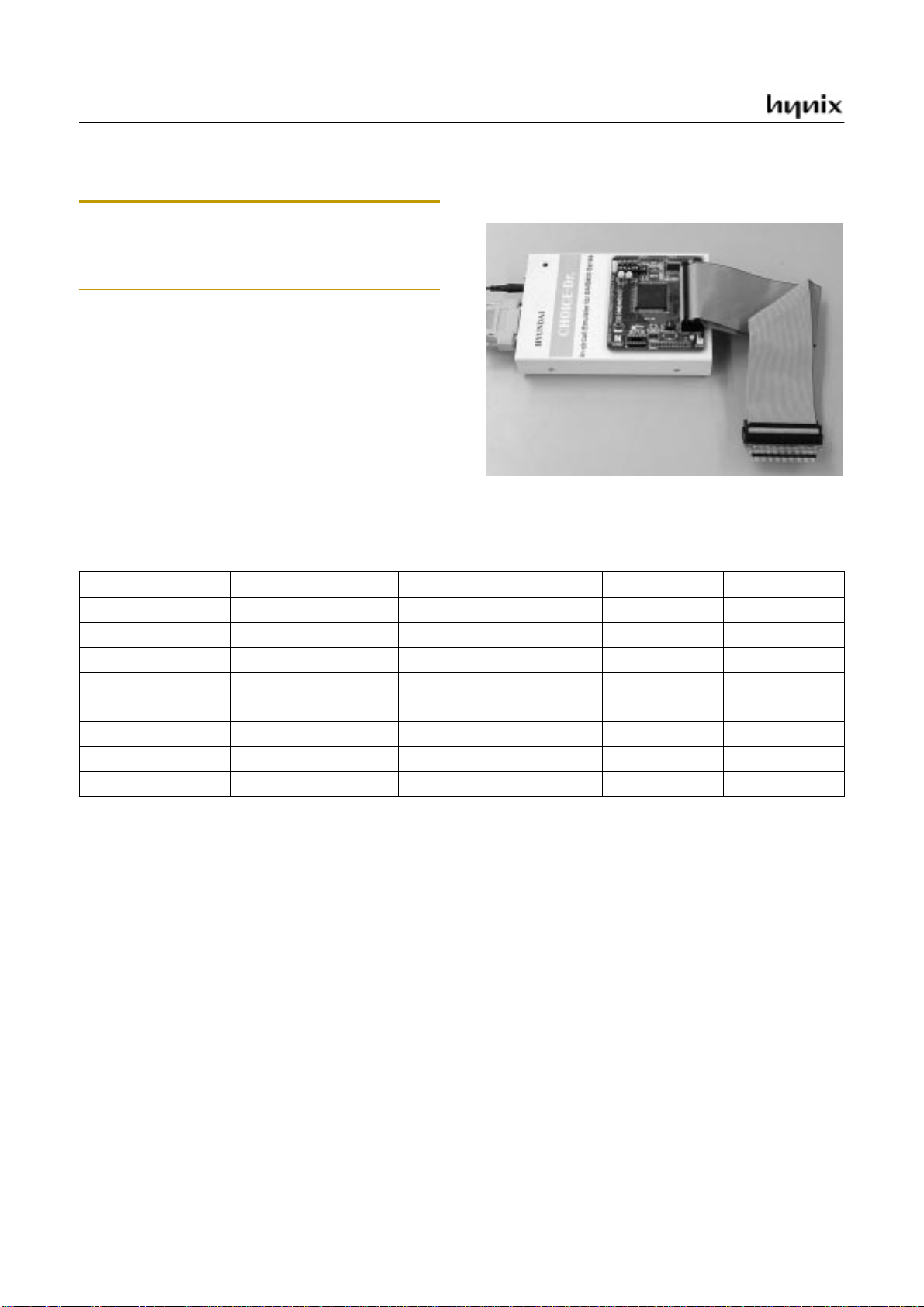
1.3 Development Tools
Note: There are several setting switches in the Emulator.
User should read carefully and do setting properly before
developing the program. Otherwise, the Emulator may not
work properly.
The HMS87C4x60 is sup po rte d b y a fu ll-f eat ured mac ro ass embler, an in-circuit emulator CHOICE-Dr.
grammers. There are two different type progra mmers such as
single type and gang type. For more de tail, refer to EP ROM Pro gramming chapter. Macro assembler operates under the MSWindows 95/98
Please contact sales part of Hynix Semiconductor.
TM
.
TM
and EPROM pro-
1.4 Ordering Information
Device na me ROM Size (bytes) RAM size Package
Mask ROM version HMS81C4260 60K bytes 1024 bytes 52SDIP
OTP ROM version HMS87C4260 60K bytes EPROM (OTP) 1024 bytes 52SDIP
Mask ROM version HMS81C4360SK 60K bytes 1024 bytes 32SKDIP
OTP ROM version HMS87C4360SK 60K bytes EPROM (OTP) 1024 bytes 32SKDIP
Mask ROM version HMS81C4360 60K bytes 1024 bytes 32PDIP
OTP ROM version HMS87C4360 60K bytes EPROM (OTP) 1024 bytes 32PDIP
Mask ROM version HMS81C4460 60K bytes 1024 bytes 42SDIP
OTP ROM version HMS87C4460 60K bytes EPROM (OTP) 1024 bytes 42SDIP
2 November 2001 Ver 1.1
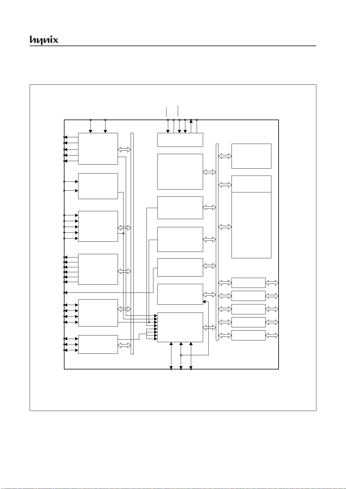
2. BLOCK DIAGRAM
VS
HS
HMS81C4x60
Vdd
RESET
Xin
Xout
Vss
TEST
YM
YS
CVBS
SCAP
R10/AN0
R11/AN1
R12/AN2
R13/AN3
R14/AN4
R30/PWM0
R31/PWM1
R32/PWM2
R33/PWM3
R34/PWM4
R35/PWM5
R36/BUZ
R40/SCL0
R41/SDA0
R42/SCL1
R43/SDA1
R24/EC2
R25/EC3
R37/TMR1
PLL
R
G
B
OSD
CLOCK
G8MC
CORE
GENERATION
/ SYSTEM
DATA
SLICER
CONTROLLER
RAM ( 1024)
PRESCALER
/BIT
ADC
WATCH DOG
MASK ROM
( User ROM
: 60KB
Font ROM
: 32KB )
TIMER
PWM
2
C
I
BUZZER
REMOCON
INTERRUPT
CONTROLLER
R4 PORT
R3 PORT
R2 PORT
R1 PORT
R0 PORT
R40 ~ R43
R30 ~ R37
R20 ~ R25
R10 ~ R14
R00 ~ R07
TIMER
R21/INT1
R22/INT2
R23/INT3
Figure 2-1 Block Diagram
November 2001 Ver 1.1 3
HMS81C4x60
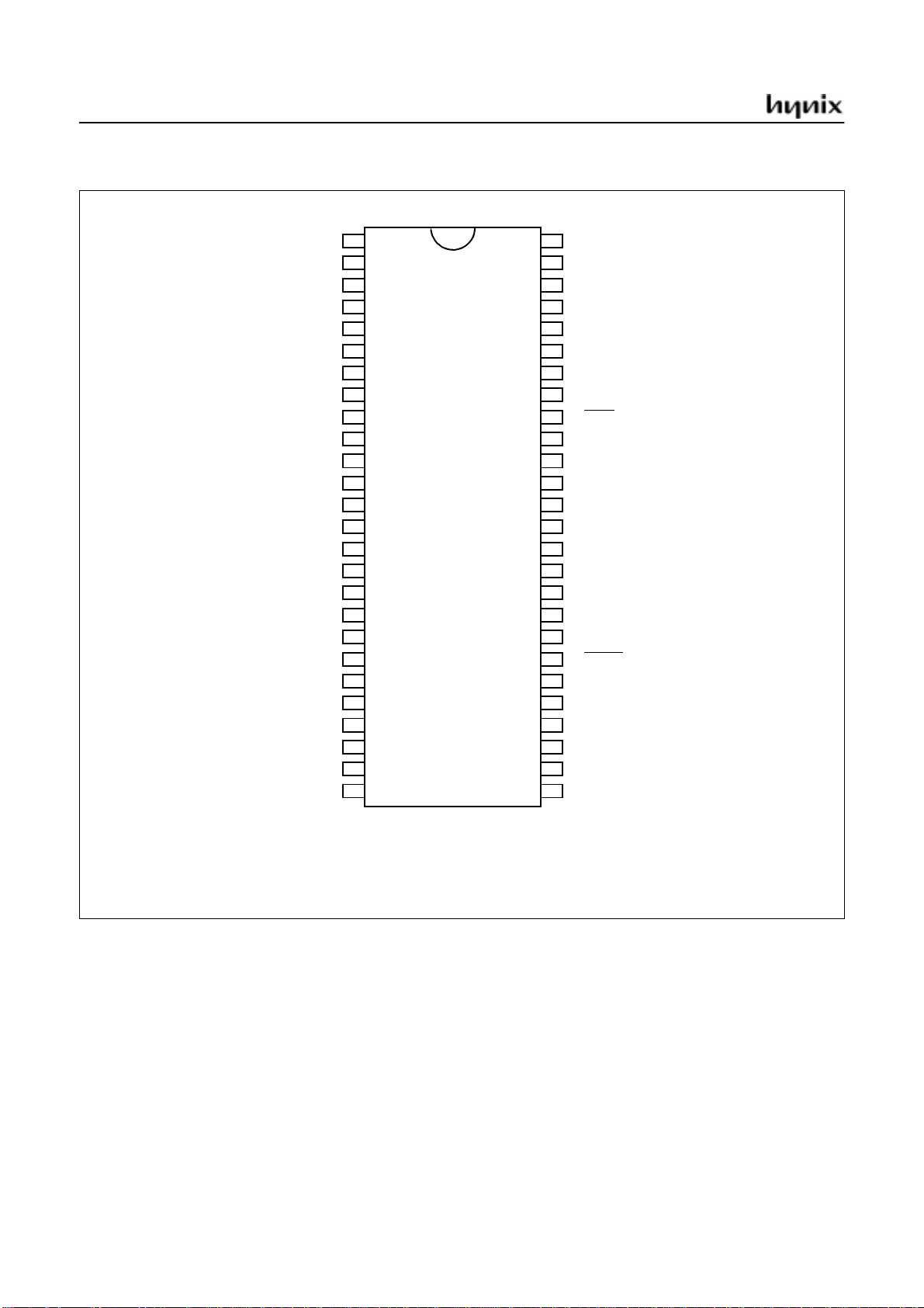
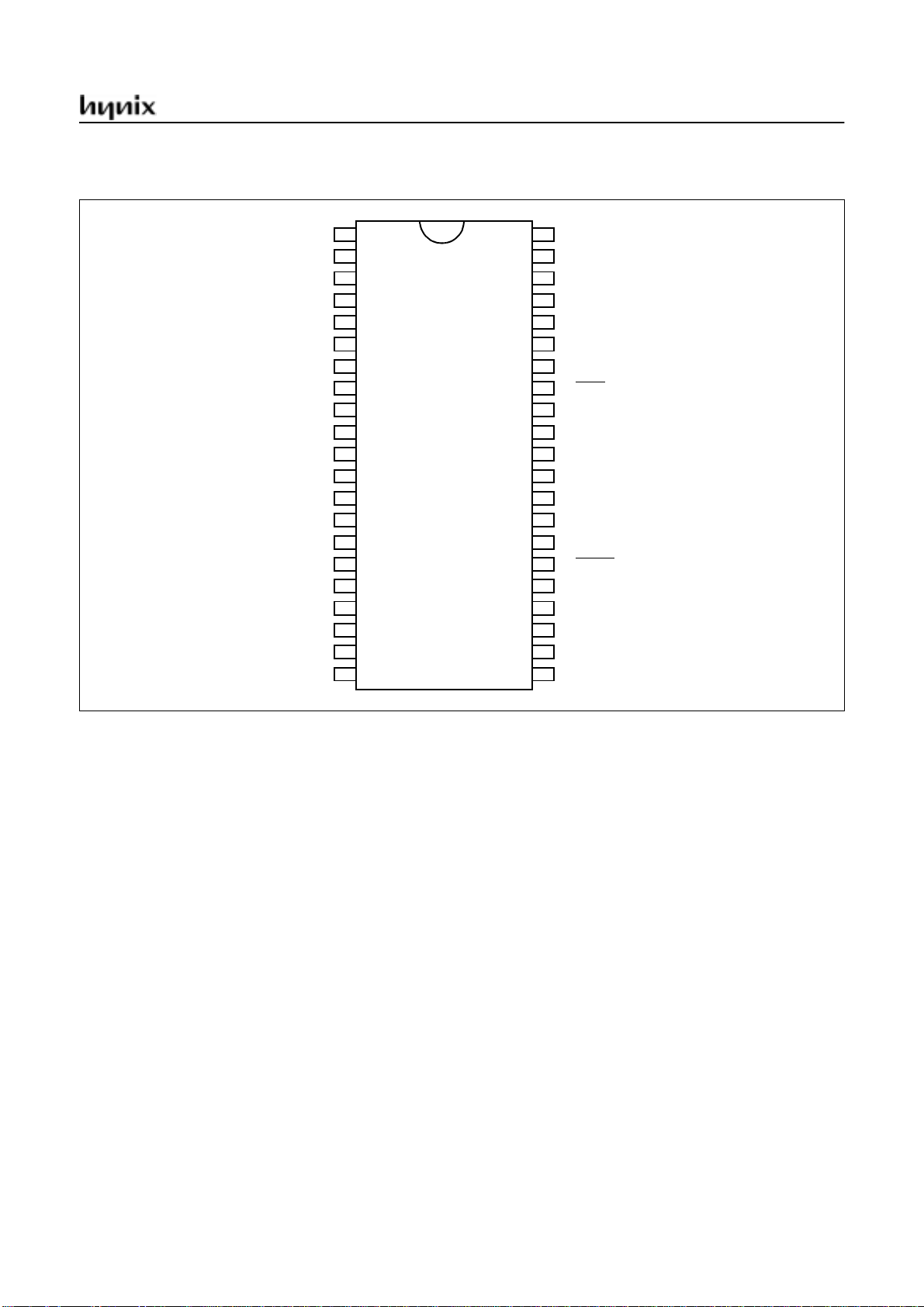
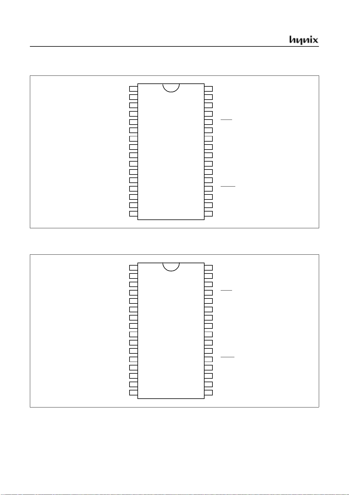
3. PIN ASSIGNMENT
R40/SCL0
R41/SDA0
R42/SCL1
R43/SDA1
R04
R05
R06
R07
VDD
R14/AD4
SCAP
CVBS
VDD
VSS
R10/AD0
R11/AD1
R12/AD2
R13/AD3
HS
VS
R20
R21/INT1
R22/INT2
R23/INT3
R24/EC2
R25/EC3
1
2
3
4
5
6
7
8
9
HMS81C4260
10
11
12
13
14
15
16
17
18
19
20
21
22
23
24
25
26
52SDIP
52
51
50
49
48
47
46
45
44
43
42
41
40
39
38
37
36
35
34
33
32
31
30
29
28
27
R30/PWM0
R31/PWM1
R32/PWM2
R33/PWM3
R34/PWM4
R35/PWM5
R36/BUZ
R37/TMR1
TEST
VSS
YM
YS
B
G
R
VDD
VSS
XIN
XOUT
RESET
R03
R02
VDD
VSS
R01
R00
Figure 3-1 52SDIP
4 November 2001 Ver 1.1
HMS81C4x60
R40/SCL0
R41/SDA0
R42/SCL1
R43/SDA1
R04
VDD
R14/AD4
SCAP
CVBS
VDD
VSS
R10/AD0
R11/AD1
R12/AD2
R13/AD3
HS
VS
R21/INT1
R22/INT2
R23/INT3
R24/EC2
1
2
3
4
5
6
7
8
9
HMS81C4460
10
11
12
13
14
15
16
17
18
19
20
21
42SDIP
42
41
40
39
38
37
36
35
34
33
32
31
30
29
28
27
26
25
24
23
22
R31/PWM1
R32/PWM2
R33/PWM3
R34PWM4
R35/PWM5
R36/BUZ
R37/TMR1
TEST
YM
YS
B
G
R
XIN
XOUT
RESET
R03
R02
R01
R00
R25/EC3
Figure 3-2 42SDIP
November 2001 Ver 1.1 5
HMS81C4x60
R40/SCL0
R41/SDA0
R42/SCL1
R43/SDA1
VDD
R14/AD4
SCAP
CVBS
VDD
VSS
R10/AD0
R13/AD3
HS
VS
R21/INT1
R22/INT2
1
2
3
4
5
6
7
HM S81C 4360SK
8
9
10
11
12
13
14
15
16
32SKDIP
Figure 3-3 32SKDIP
32
31
30
29
28
27
26
25
24
23
22
21
20
19
18
17
R33/PWM3
R34/PWM4
R35/PWM5
R37/TMR1
TEST
YM
YS
B
G
R
XIN
XOUT
RESET
R02
R24/EC2
R23/INT3
R40/SCL0
R41/SDA0
R42/SCL1
R43/SDA1
VDD
R14/AD4
SCAP
CVBS
VDD
VSS
R10/AD0
R11/AD1
R12/AD2
R13/AD3
HS
VS
1
2
3
4
5
6
7
8
HMS81C4360
9
10
11
12
13
14
15
16
32PDIP
Figure 3-4 32PDIP
32
31
30
29
28
27
26
25
24
23
22
21
20
19
18
17
R34PWM4
R35PWM5
R37/TMR1
TEST
YM
YS
B
G
R
XIN
XOUT
RESET
R02
R24/EC2
R23/INT3
R21/INT1
6 November 2001 Ver 1.1
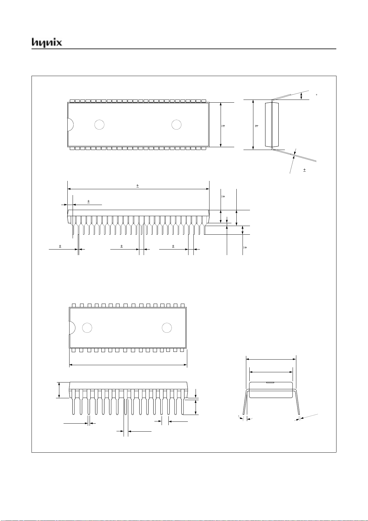
4. PACKAGE DIAGRAM
HMS81C4x60
HYNIX
HMS81C4260
1
45.97
0.13
0.76
0.47 0.13 1.02 0.25
0.13
1.778
0.25
2752
13.97
0.25
26
3.81 0.13
0.50 Min.
15.24
0.25
4.38 Max.
3.24
0.20
UNIT: mm
0 ~ 15
0.25 0.05
0.2 max
1
0.022
0.015
HYNIX
HMS81C4360
1.665
1.645
0.065
0.045
1732
16
0.1 BSC
MIN 0.015
0.140
0.120
TYP 0.600 BSC
0 ~ 15°
0.550
0.530
UNIT: inch
0
.
0
.
0
2
1
8
0
0
November 2001 Ver 1.1 7
HMS81C4x60
HYNIX
HMS81C4460
1
0.13
0.76
0.47 0.13 1.02 0.25
36.83
0.13
1.778
0.25
2242
13.97
0.25
21
3.81 0.13
0.50 Min.
15.24
0.25
4.38 Max.
3.24
0.20
UNIT: mm
0 ~ 15
0.25 0.05
32
HY NIX
HM S81C4360S K
1
27.68
0.76
0.13
0.47 0.13 1.02 0.2 5
0.13
17
16
1.778
0.25
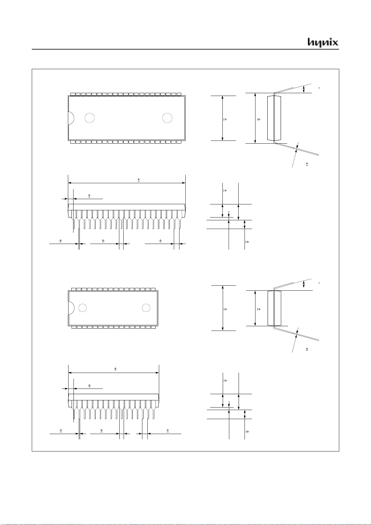
Figure 4-1 Package Diagram
10.16
0.25
3.81 0.13
0 ~ 15
8.89
0.25
0.25 0.0 5
4.38 Max.
3.24
0.50 Min.
0.20
UNIT: mm
8 November 2001 Ver 1.1

5. PIN FUNCTION
HMS81C4x60
VDD: Supply voltage.
V
: Circuit ground.
SS
TEST
: Used for shipping inspection of the IC. For normal
operation, it should not be connected .
RESET
X
: Reset the MCU.
: Input to the inverting oscillator amplifier and input to
IN
the internal main clock operating circuit.
X
: Output from the inverting oscillator amplifier.
OUT
R00~R07: R0 is an 8-bit bidirectional I/O port. R0 pin s 1
or 0 written to the Port Direction Register can be used as
outputs or inputs.
R10~R14: R1 is a 5-bit read only port. R1 pins 1 or 0 writ ten to the Port Direction Register can be used as inputs.
In addition, R1 serves the functions of the various following special features.
Port pin Alternate function
R10
R11
R12
R13
R14
AD0 (A/D converter input 0)
AD1 (A/D converter input 1)
AD2 (A/D converter input 2)
AD3 (A/D converter input 3)
AD4 (A/D converter input 4)
R20~R25: R2 is a 6-bit CMOS bidirectional I/O port. Each
pins 1 or 0 written to the their Port Direction Regist er can
be used as outputs or inputs.
R30~R37: R3 is 8-bit CMOS bidirectional I/O port. R0
pins 1 or 0 written to the Port Direction Register can be
used as outputs or inputs.
In addition, R3 serves the functions of the various follow ing special features.
Port pin Alternate function
R30
R31
R32
R33
R34
R35
R36
R37
PWM0 (Pulse Width Modulation outp ut 0)
PWM1 (Pulse Width Modulation outp ut 1)
PWM2 (Pulse Width Modulation outp ut 2)
PWM3 (Pulse Width Modulation outp ut 3)
PWM4 (Pulse Width Modulation outp ut 4)
PWM5 (Pulse Width Modulation outp ut 5)
with 14bit resolution
BUZ (Buzzer output)
TMR1 (Timer Interrupt 1)
R40~R43: R4 is a 4- bit open drain I/ O por t. Each pi ns 1 or
0 written to the their Port Direction Register can b e used as
outputs or inputs.
In addition, R4 serves the functions of the various follow ing special features.
Port pin Alternate function
2
R40
R41
R42
R43
SCL0 (I
SDA0 (I
SCL1 (I
SDA1 (I
C Clock 0)
2
C Data0)
2
C Clock 1)
2
C Data 1)
In addition, R2 serves the functions of the various following special features.
Port pin Alternate function
R21
R22
R23
R24
R25
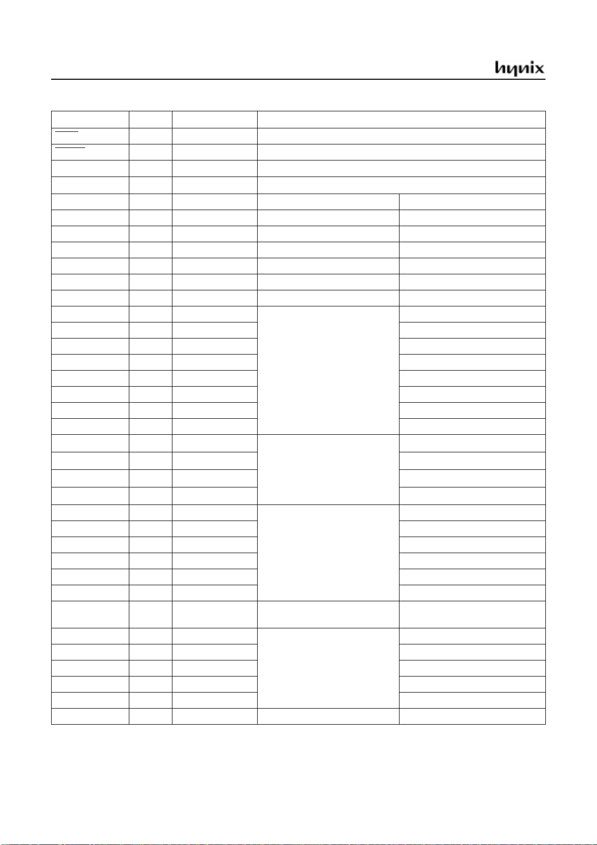
PIN NAME Pin No. In/Out Function
V
DD
V
SS
INT1 (External interrupt input 1)
INT2 (External interrupt input 2)
INT3 (External interrupt input 3)
EC2 (Event counter input 2)
EC3 (Event counter input 3)
9,13,30,
37
14,29,
36,43
- Supply voltage
- Circuit ground
Table 5-1 Port Function Description
R,G,B: R,G,B are output port. Each pins controls Red,
Green, Blue color control.
YM,YS: YM,YS are CMOS output port. Each pins controls Background, Edge control.
HS,VS: HS,VS are CMOS input port. Each pins Vertical
Sync. input and Horizaltal Sync. inputs.
CVBS: CVBS is a CVBS(Composit Video in) signal input
pin.
November 2001 Ver 1.1 9
HMS81C4x60
PIN NAME Pin No. In/Out Function
TEST 44 I TEST signal input (internal pull up resister)
RESET
X
IN
X
OUT
HS 19 I Horisontal Sync. input
VS 20 I Vertical Sync. input
R 38 O Red signal output
G 39 O Green signal output
B 40 O Blue signal output
YS 41 O Edge signal output
YM 42 O Background signal output
R30/PWM0 52 I/O
R31/PWM1 51 I/O 8bit PWM (pull up)
R32/PWM2 50 I/O 8bit PWM (pull up)
R33/PWM3 49 I/O 8bit PWM (pull up)
R34/PWM4 48 I/O 8bit PWM
R35/PWM5 47 I/O 14bit PWM
R36/BUZ 46 I/O Buzzer (pull up)
R37/TMR1 45 I/O Timer Interrupt 1
R40/SCL0 1 I/O
R41/SDA0 2 I/O
R42/SCL1 3 I/O
R43/SDA1 4 I/O
R20 21 I/O
R21/INT1 22 I/O External interrupt input 1
R22/INT2 23 I/O External interrupt input 2 (pull up)
R23/INT3 24 I/O External interrupt input 3
R24/EC2 25 I/O Event counter input 2
R25/EC3 26 I/O Event counter input 3 (pull up)
SCAP 11 I
R10/AD0 15 I
R11/AD1 16 I Analog input 1
R12/AD2 17 I Analog input 2
R13/AD3 18 I Analog input 3
R14/AD4 10 I Analog input 4
CVBS 12 I Composit video input
33 I Reset signal input
35 I Main oscillation input
34 O Main oscillation output
PWM functions
2
I
C functions (open drain)
External interrupt functions
A/D conversion functions
8bit PWM (pull up)
I2C Serial clock 0
2
C Serial data 0
I
2
C Serial clock 1
I
2
C Serial data 1
I
(pull up)
Data slicer comparation reference
voltage
Analog input 0
Table 5-1 Port Function Description
10 November 2001 Ver 1.1

PIN NAME Pin No. In/Out Function
HMS81C4x60
R00 27 I/O
R01 28 I/O (normal I/O, pull up)
R02 31 I/O (normal I/O)
R03 32 I/O (normal I/O, pull up)
R04 5 I/O (open drain, pull up)
R05 6 I/O (open drain, pull up)
R06 7 I/O (open drain, pull up)
R07 8 I/O (open drain, pull up)
Table 5-1 Port Function Description
Digital I/O functions
(normal I/O, pull up)
November 2001 Ver 1.1 11
HMS81C4x60
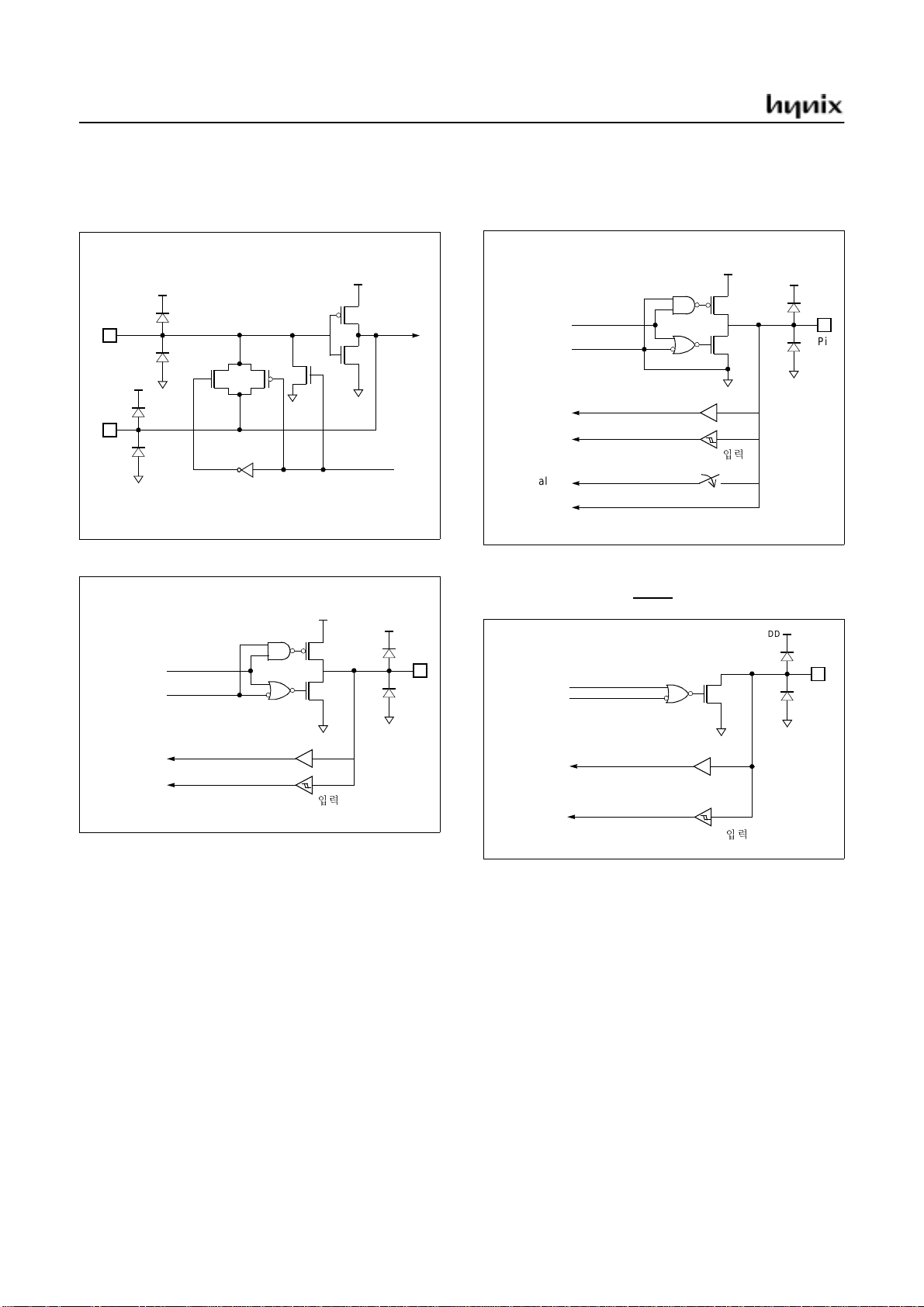
6. PORT STRUCTURES
XIN, X
OUT
V
DD
X
IN
V
DD
V
SS
X
OUT
V
SS
Main frequency
clock
V
SS
R03~R00,R37~R30,HS,VS,YS,YM
Data out
Out Enable
R14~10, CVBS
V
V
DD
Data out
Out Enable
V
SS
Data in
Data in
STOP
Analog in
Analog in
V
DD
V
DD
R07~R04, R43~R40, TEST
I/O
Pin
Data out
Out Enable
DD
V
SS
SchmittÛ{
V
DD
I
Pin
V
SS
V
DD
I/O
Pin
Data in
Data in
Schmitt
V
V
SS
SS
V
SS
V
SS
Data in
Û
{
Data in
Schmitt Û{
12 November 2001 Ver 1.1
HMS81C4x60
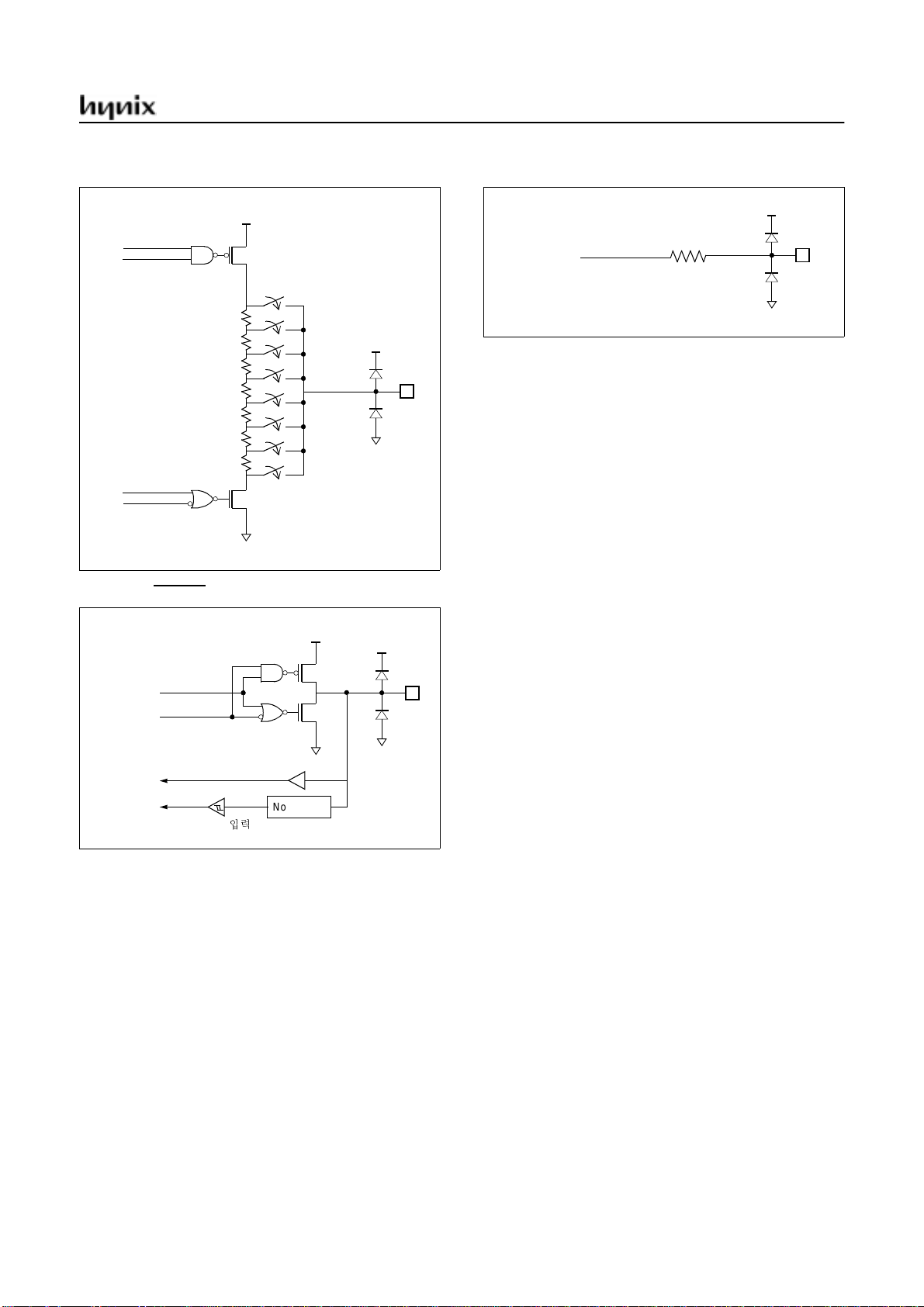
R,G,B
R25~R20, RESET
SCAP
V
V
DD
Data In
V
DD
I/O
Pin
V
SS
V
SS
DD
I/O
Pin
V
SS
Data out
Out Enable
Data in
Data in
Schmitt
V
DD
V
SS
Noise Filter
Û
{
V
DD
I/O
Pin
V
SS
November 2001 Ver 1.1 13
HMS81C4x60
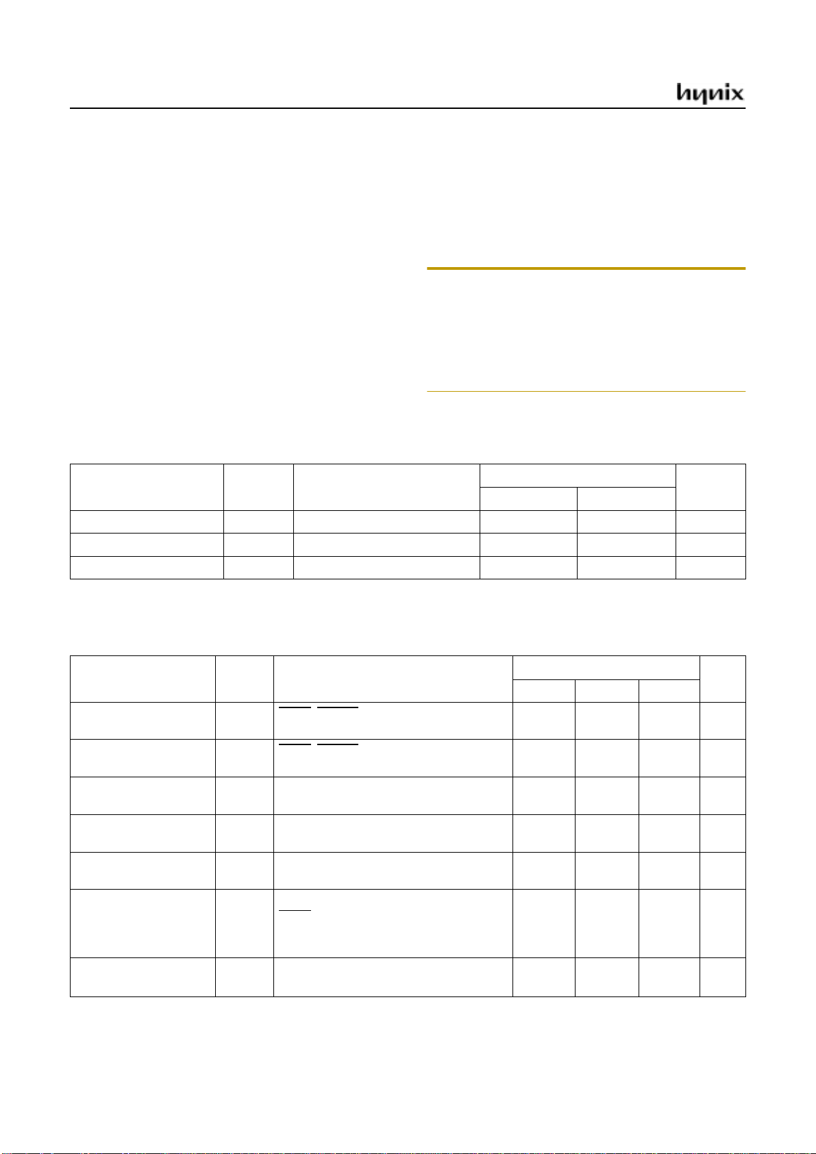
7. ELECTRICAL CHARACTERISTICS
7.1 Absolute Maximum Ratings
Supply voltage...........................................-0.3 to +6.0 V
Storage Temperature ................................-40 to +125 °C
Voltage on any pin with respect to Ground (V
................................ ............................... -0.3 to V
SS
)
DD
+0.3
Maximum current out of Vss pin.........................160 mA
Maximum current into V
Maximum current sunk by(I
Maximum output current sourced by (I
pin ..........................160 mA
DD
per I/O Pin) .........20 mA
OL
per I/O Pin)
OH
.................................................................................8 mA
7.2 Recommended Operating Conditions
Parameter Symbol Condition
Supply Voltage
Operating Frequency
Operating Temperature
V
f
T
DD
XIN
OPR
VDD=4.5~5.5V
f
XIN
7.3 DC Electrical Characteristics
=4MHz
Maximum current (ΣI
Maximum current (ΣI
)....................................100 mA
OL
)......................................80 mA
OH
Note: Stresses above those listed under “Absolute Maximum Ratings” may cause per manent damage to the d evice. This is a stress ra ting only and functional ope r ati on of
the device at any oth er c ond iti ons ab ov e tho se ind ic ated in
the oper ati o na l se c ti ons of this s pe c ifi ca t io n i s no t i m pl ie d .
Exposure to absolute maximum rating conditions for extended periods may affect device reliability.
Specifications
Unit
Min. Max.
4.5 5.5 V
-4.0(typical)MHz
-10 70
C
°
(TA=-10~70°C, VDD=4.5~5.5V)
Parameter Symbol Condition
High level input voltage
Low level input voltage
High level output voltage
Low level output voltage
Supply current in
ACTIVE mode
pull-up lekage current
High input leakage
current
V
V
V
V
I
I
RUP
I
,
TEST, RESET, Xin, R0, R1, R2, R3,
IH
HS, VS
TEST, RESET, Xin, R0, R1, R2, R3,R4
IL
HS, VS
I
= -5mA
OH
OH
R0, R1, R2, R3, YS, YM
I
= 5mA
OL
OL
R0, R1, R2, R4
V
DD
IZH
DD
VDD = 5.5v, V
, R00, R01, R03, R04, R05, R06,
TEST
PIN
= 0.4V
R07, R20, R22, R25, R30, R31, R32, R33
R36
V
= 5.5V, V
DD
PIN
= V
DD
All input, I/O pins ex cept X
Specifications
Unit
Min. Typ. Max.
0.8 V
DD
-
0-
VDD - 1
-
--V
-1.0v
V
DD
0.12 V
DD
V
V
-4080mA
-1.5 -400
IN
-5 - 5
A
µ
A
µ
14 November 2001 Ver 1.1

HMS81C4x60
Parameter Symbol Condition
V
Low input leakage
current
RAM data retention
voltage
Hysterisis
Comparator operating
range
Comparator resolution
RGB DAC
Resolution 1
I
IZL
V
RAM
Vt+ ~
Vt-
V
rCVBS
V
aCVBS
RGB
R1
= 5.5V, V
DD
All input, I/O pins ex cept X
V
DD
, RESET, Xin, HS, VS, R07 ~ R00,
TEST
R21, R23, R24, R25, R37 ~ R30
V
= 5V
DD
CVBS pin
V
= 5V
DD
CVBS pin
V
= 5V
DD
No in/out current in R,G,B pin
RGB DAC On
No in/out current in R,G,B pin
Level 0
Level 1
RGB DAC
Output voltage
V
RGB
Level 2
Level 3
Level 4
Level 5
Level 6
Level 7
V
= 5V
DD
RGB V
RGB V
oh
ol
V
V
ohrgb
olrgb
RGB DAC On
Level 7
= -3mA
I
OH
V
= 5V
DD
RGB DAC On
Level 0
= 3mA
I
OL
PIN
= 0V
, OSC1
IN
Specifications
Unit
Min. Typ. Max.
-5 - 5
A
µ
1.2 - - V
1.0 - - V
1.2 - 3.5 V
- - 0.08 V
--5%
3/40V
dd
5/40V
dd
8/40V
dd
12/40V
17/40V
23/40V
30/40V
38/40V
dd
dd
dd
dd
dd
V
3.1 3.5 3.9 V
0.4 0.6 0.8 V
7.4 AC Characteristics
(TA=-10~70°C, VDD=5V±10%, VSS=0V)
Parameter Symbol Pins
Crystal oscillator Frequency
External Clock Pulse Width
External Clock Transition Time
f
XIN
t
MCPW
t
SCPW
t
MRCP,tMFCP
t
SRCP,tSFCP
X
IN
X
IN
S
CLK
X
IN
S
CLK
Specifications
Unit
Min. Typ. Max.
345MHz
180 - 350 nS
0.5 -
S
µ
- - 20 nS
- - 20 nS
November 2001 Ver 1.1 15
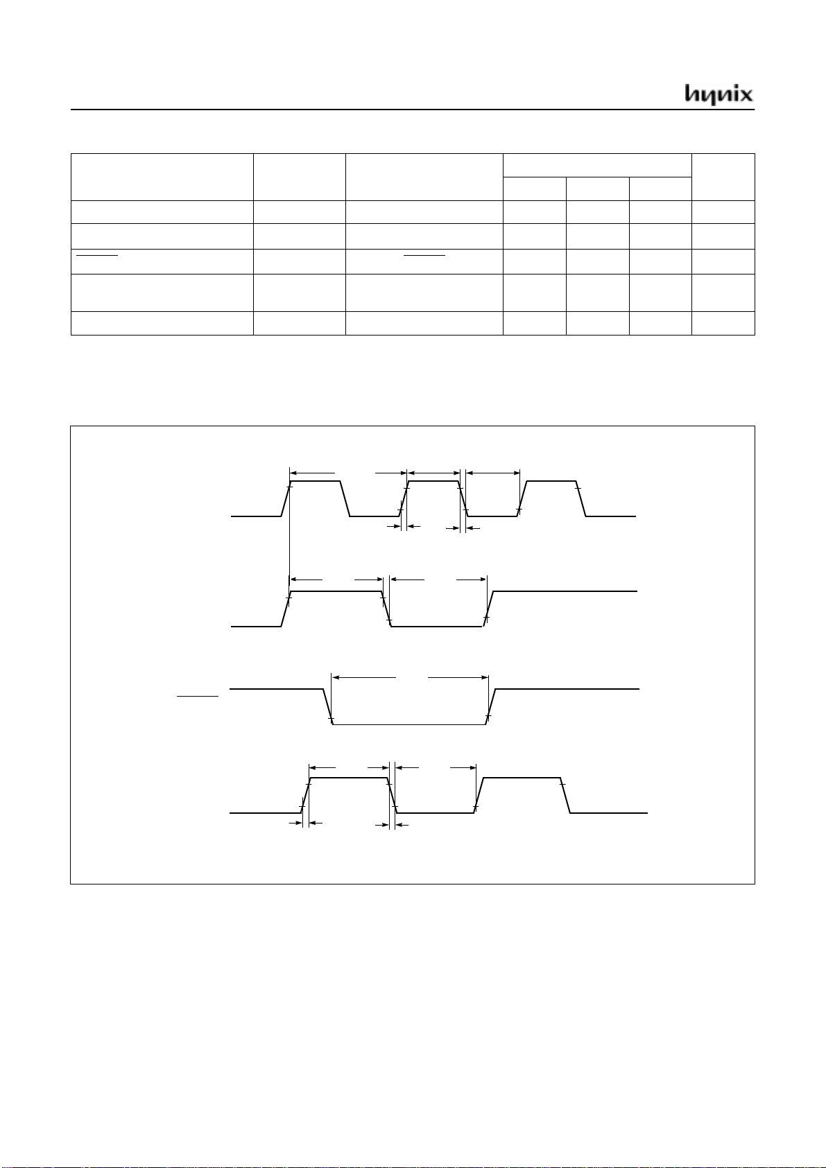
HMS81C4x60
Parameter Symbol Pins
Oscillation Stabilizing Time
Interrupt Pulse Width
RESET Input Width
Event Counter Input Pulse
Width
Event Counter Transition Time
1. t
is one of 1/f
SYS
main clock operation mode,
XIN
X
IN
t
ST
t
IW
t
RST
t
ECW
t
REC,tFEC
Specifications
Unit
Min. Typ. Max.
XIN, X
OUT
INT1~3 2 - RESET 8--
EC2, EC3 2 - -
--20mS
1
t
SYS
1
t
SYS
1
t
SYS
EC2, EC3 - - 20 nS
t
t
MRCP
MCPW
1/f
XIN
t
MFCP
t
MCPW
0.5V
-0.5V
V
DD
INT1 ~ 3
RESET
EC2, EC3
0.8V
t
REC
t
IW
DD
t
RST
t
ECW
t
FEC
Figure 7-1 Timing Chart
t
ECW
t
IW
0.2V
DD
0.2V
DD
0.8V
DD
0.2V
DD
16 November 2001 Ver 1.1
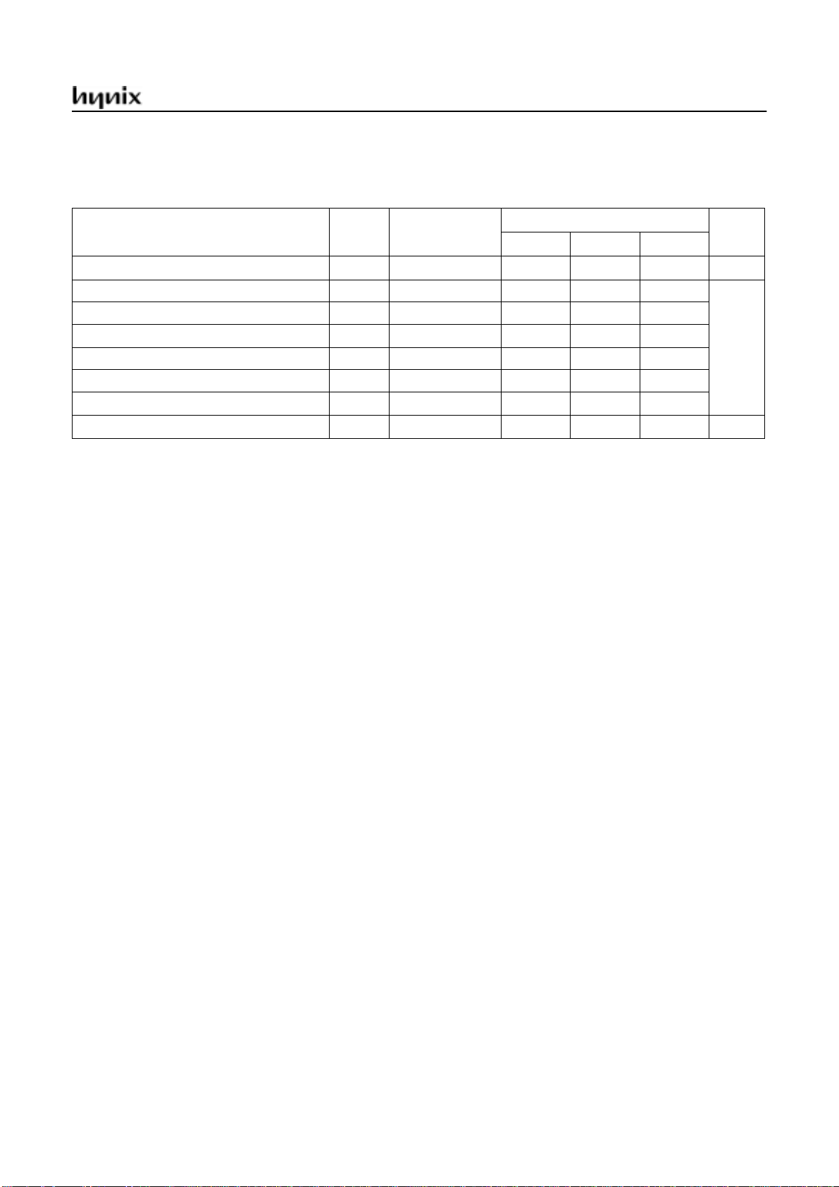
7.5 A/D Converter Characteristics
(TA=25°C, VDD=5V, VSS=0V)
HMS81C4x60
Parameter Symbol Condition
Analog Input Voltage Range
Overall Accuracy CAIN - Non Linearity Error NNLE - Differential Non Linearity Error NDNLE - Zero Offset Error NZOE - Full Scale Error NFSE - Gain Error NGE - Conversion Time TCONV
V
AN
f
MAIN
-
=4MHz
Min. Typ. Max.
VSS-0.3
Specifications
-
1.5
±
1.5
±
1.5
±
0.5
±
0.75
±
1.5
±
--15µS
VDD+0.3
2.5
±
2.5
±
2.5
±
2.0
±
1.0
±
2.0
±
Unit
V
LSB
November 2001 Ver 1.1 17
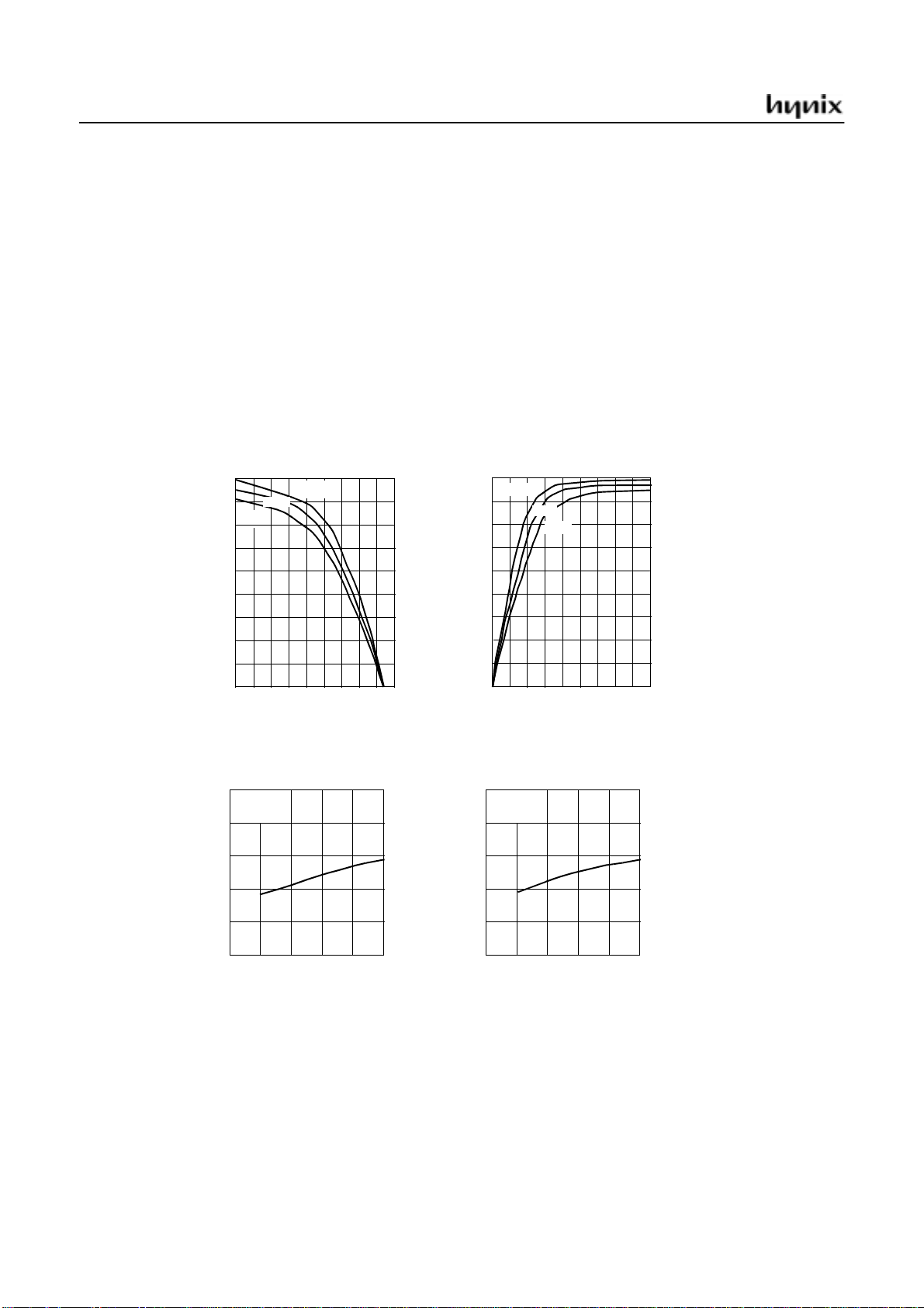
HMS81C4x60
7.6 Typical Characteristics
These graphs and tables are for design guidance only and
are not tested or guaranteed.
In some graphs or tables, the datas presented are outside specified operating range (e.g. outside specified
VDD range). This is for information only and devices
are guaranteed to operate properly only within the
specified range.
I
OH
(mA)
-16
-14
-12
-10
I
OH
70°C
-8
-6
-4
-2
0
V
−
OH
-20°C
25°C
2.0 3.0
, VDD=5.2V
4.0
5.0
V
(V)
OH
The data is a statistical summary of data collected on units
from different lots over a period of time. “Typical” represents the mean of the distribution while “max” or “min”
represents (mean + 3σ) and (mean − 3σ) r espectively
where σ is standard deviation
I
OL
(mA)
40
30
20
10
I
OL
-20°C
, VDD=5.2V
V
−
OL
25°C
70°C
1.0 3.02.0
4.0
V
(V)
OL
V
V
−
DD
Hysterisis
f
=4MHz
MAIN
Ta=25°C
44.5
IH
55.5
V
DD
(V)
6
V
V
−
DD
IH
V
IH1
f
=4MHz
MAIN
(V)
Ta=25°C
4
3
2
1
0
44.5
55.5
V
DD
(V)
6
V
IH2
(V)
4
3
2
1
0
18 November 2001 Ver 1.1
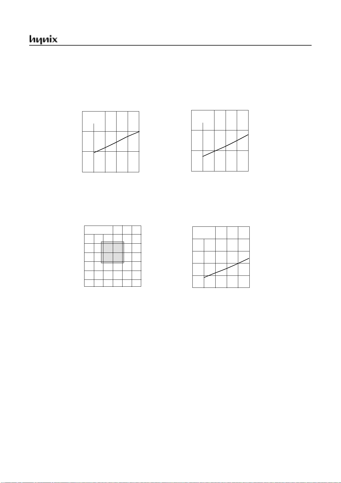
HMS81C4x60
V
V
−
DD
V
V
−
DD
IL
V
V
IL1
f
=4MHz
MAIN
(V)
Ta=25°C
IL1
(V)
Hysterisis
f
=4MHz
MAIN
Ta=25°C
IL
3
2
1
44.5
Operating Area
f
MAIN
Ta= -20~70°C
(MHz)
(Main-clock)
6
5
4
3
2
1
0
44.555.5 6.5
55.5
6
3
2
V
DD
(V)
6
1
44.5
55.5
V
DD
(V)
6
Normal Mode (Main opr.)
I
V
−
DD1
I
DD
(mA)
60
50
40
30
V
(V)
DD
20
DD
Ta=25°C
f
=4MHz
MAIN
44.555.56
V
DD
(V)
November 2001 Ver 1.1 19
HMS81C4x60
8. MEMORY ORGANIZATION
The GMS81C4x60 has separate address spaces for Program memory, Data Memory and D isplay memory. Program memory can only be read, not written to. It can be up
8.1 Registers
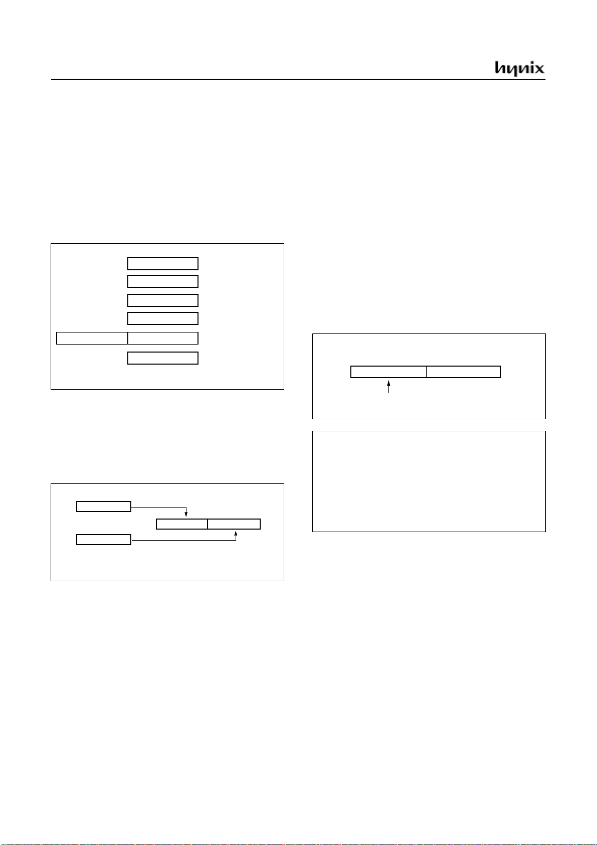
This device has six registers that are the Program Counter
(PC), a Accumulator (A), two index registers (X, Y), the
Stack Pointer (SP), and the Program Status Word (PSW).
The Program Counter consists of 16-bit register.
A
X
Y
SP
PCLPCH
PSW
Figure 8-1 Configuration of Registers
Accumulator: The Accumulato r is the 8-bit gen eral purpose register, used for data operation such as transfer, temporary saving, and conditional judgement, etc.
The Accumulator can be used as a 16-bit register with Y
Register as shown below.
ACCUMULATOR
X REGISTER
Y REGISTER
STACK POINTER
PROGRAM COUNTER
PROGRAM STATUS
WORD
to 60K bytes of Program mem ory. Data memory can be
read and written to up to 1024 bytes including the stack area. Font memory has prepared 32K bytes for OSD.
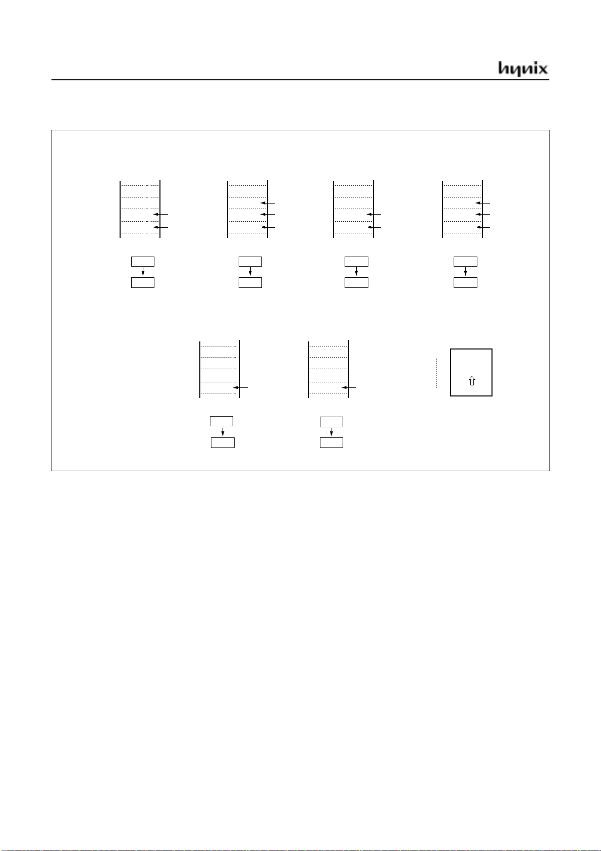
Generally, SP is automatically updated when a subrout ine
call is executed or an interrupt is accepted. However, if it
is used in excess of the stack area permitted by the data
memory allocating configuration, the user-processed data
may be lost.
The stack can be located at any position within 0 0
to FF
H
of the internal data memory. The SP is not initialized by
hardware, requiring to write the initial value (the location
with which the use of the stack starts) by using the initialization routine. Normally, the initial value of “FF
H”
is
used.
Stack Address (00
15 087
1
Hardware fixed
~ FFH)
H
SP
Caution:
The Stack Pointer must be initialized by software be-
cause its value is undefined after RESET.
Example: To initialize the SP
H
Y
Y A
A
LDX #0FFH
TXSP ; SP ← FFH
Program Counter: The Program Count er is a 16-bit wid e
Two 8-bit Registers can be used as a “YA” 16-bit Register
which consists of two 8-bit registers, PCH and PCL. This
counter indicates the address of the next instruction to be
Figure 8-2 Configuration of YA 16-bit Register
X, Y Registers: In the addressing mode which uses these
index registers, the register conten ts a re added to the specified address, which becomes the actual address. These
modes are extremely effective for referencing subroutine
tables and memory tables . The index regi sters also h ave increment, decrement, comparison and data transfer functions, and they can be used as simple accumulators.
Stack Pointer: The Stack Pointer is an 8-bit register used
for occurrence interrupts and calling out subroutines. Stack
Pointer identifies the location in the stack to be accessed
(save or restore).
executed. In reset state, the program counter has reset routine address (PC
:0FFH, PCL:0FEH).
H
Program Status Word: The Program Status Word (PSW)
contains several bits that reflect the current state of the
CPU. The PSW is described in Figure 8-3. It contains the
Negative flag, the Overflow flag, the Break flag the Half
Carry (for BCD operation), the Interrupt enable flag, the
Zero flag, and the Carry flag.
[Carry flag C]
This flag stores any carry or borrow from the ALU of CPU
after an arithmetic operation and is also changed by the
Shift Instruction or Rotate Instruction.
20 November 2001 Ver 1.1

HMS81C4x60
[Zero flag Z]
This flag is set when the result of an arithmetic operat ion
MSB LSB
N
PSW
NEGATIVE FLAG
OVERFLOW FLAG
SELECT DIRECT PAGE
when g=1, page is addressed by RPR
BRK FLAG
Figure 8-3 PSW (Program Status Word) Register
V G B H I Z C
[Interrupt disable flag I]
This flag enables/disables all interrupts except interrupt
caused by Reset or software BRK instruction. All interrupts are disabled when cleared to “0”. This flag immediately becomes “0” when an interrupt is served. It is set by
the EI instruction and cleared by the DI instruction.
or data transfer is “0” and is cleared by any other result.
RESET VALUE : 00
CARRY FLAG RECEIVES
CARRY OUT
ZERO FLAG
INTERRUPT ENABLE FLAG
HALF CARRY FLAG RECEIVES
CARRY OUT FROM BIT 1 OF
ADDITION OPERLANDS
H
This flag assigns RAM page for direct addressing mode. In
the direct addressing mode, addressing area is from zero
page 00
to 0FFH when this flag is "0". If it is set to "1",
H
addressing area is assigned by RPR register (address
0F3
). It is set by SETG instruction and cleared by CLRG.
H
[Overflow flag V]
[Half carry flag H]
After operation, this is set when there is a carry from bit 3
of ALU or there is no borrow from bit 4 of ALU. This bit
can not be set or cleared except CLRV instruction with
Overflow flag (V).
[Break flag B]
This flag is set by software BRK instruction to distinguish
BRK from TCALL instruction with the same vector address.
[Direct page flag G]
This flag is set to “1” when an overflow occurs as the result
of an arithmetic operation involving signs. An overflow
occurs when the result of an addition or subtraction ex-
ceeds +127 (7F
) or −128 (80H). The CLRV instruction
H
clears the overflow flag. There is no set instruction. When
the BIT instruction is executed, bit 6 of memory is copied
to this flag.
[Negative flag N]
This flag is set to match the sign bit (bit 7) status of the re-
sult of a data or arithmetic operation. When the BIT in-
struction is executed, bit 7 of memory is copied to this flag.
November 2001 Ver 1.1 21
HMS81C4x60
At execution of a
CALL/TCALL/PCALL
01BC
01BD
01BE
01BF
SP before
execution
SP after
execution
PCL
PCH
01BF
01BD
Push
down
01BC
01BD
SP before
execution
SP after
execution
01BC
01BD
01BE
01BF
At execution
of PUSH instruction
PUSH A (X,Y,PSW)
01BE
01BF
A
01BF
01BE
At acceptance
of interrupt
PSW
PCL
PCH
01BF
01BC
Push
down
Push
down
01BC
01BD
01BE
01BF
At execution
of RET instruction
01BC
01BD
01BE
01BF
At execution
of POP instruction
POP A (X,Y,PSW)
PCL
PCH
01BD
01BF
A
01BE
01BF
Pop
up
Pop
up
At execution
of RETI instruction
01BC
0100
01BF
PSW
H
H
01BD
01BE
01BF
PCL
PCH
01BC
01BF
Stack
depth
Pop
up
Figure 8-4 Stack Operation
22 November 2001 Ver 1.1
8.2 Program Memory
HMS81C4x60
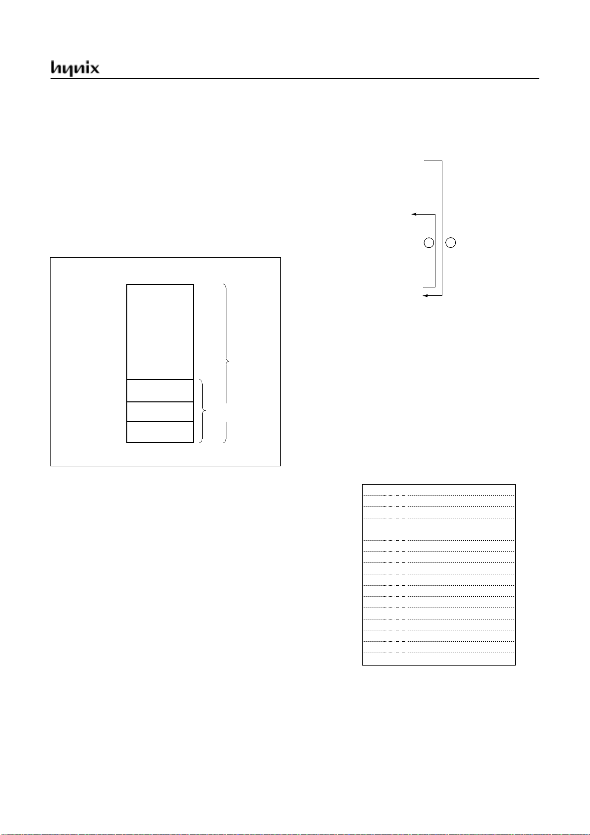
A 16-bit program counter is capable of addressing up to
64K bytes, but this device has 6 0K bytes program memory
space only physically implemented. Accessing a location
above FFFF
will cause a wrap-around to 0000H.
H
Figure 8-5 shows a map of Program Memory. After reset,
the CPU begins execution from reset vector which is stored
in address FFFE
and FFFFH as shown in Figure 8-6.
H
As shown in Figure 8-5, each area is assigned a fix ed location in Program Memory. Program Memory area contains
the user program.
1000
H
PROGRAM
FEFF
FF00
FFC0
FFDF
FFE0
FFFF
H
H
H
H
H
INTERRUPT
VECTOR ARE A
H
TCALL
AREA
MEMORY
PCALL
AREA
Example: Usage of TCALL
LDA #5
TCALL 15 ;
:;
:;
;
;TABLE CALL ROUTINE
;
FUNC_A: LDA LRG0
RET
;
FUNC_B: LDA LRG1
RET
;
;TABLE CALL ADD. AREA
;
ORG 0FFC0H ;
DW FUNC_A
DW FUNC_B
1BYTE INSTRUCTION
INSTEAD OF 2 BYTES
NORMAL CALL
1
2
TCALL ADDRESS AREA
The interrupt causes the CPU to jum p to specific location,
where it commences the execution of the service routine.
The External interrupt 1, for example, is assigned to location 0FFF8
interval: 0FFF6
0FFE8
Any area from 0FF00
. The interrupt service locations spaces 2-byte
H
and 0FFF7H for External Interru pt 2,
H
and 0FFE9H for External Interrupt 3, etc.
H
to 0FFFFH, if it is not going to be
H
used, its service location is available as general purpose
Program Memory.
Figure 8-5 Program Memory Map
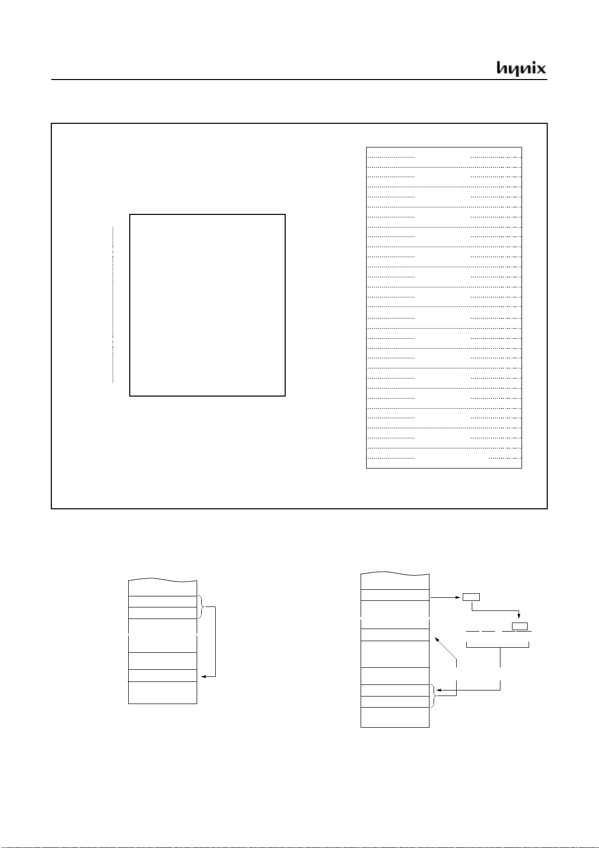
Page Call (PCALL) area contains subroutine program to
reduce program byte length by using 2 bytes PCALL instead of 3 bytes CALL instruction. If it is frequently called,
it is more useful to save program byte length .
Table Call (TCALL) c auses the CPU to jump to each
TCALL address, where it commences the execution of the
service routine. The Table Call service area spaces 2-byte
for every TCALL: 0FFC0
for TCALL15, 0FFC2H for
H
TCALL14, etc., as shown in Figure 8-7.
Address Vector Area Memo ry
0FFE0
H
E2
E4
E6
E8
EA
EC
EE
F0
F2
F4
F6
F8
FA
FC
FE
2
C Bus Interface Interrupt Vector
I
-
Basic Interval Timer Interrupt Vector
Watchdog Timer Interrupt Vector
External Interrupt 3/4 Vector
Timer/Counter 3 Interrupt Vector
Timer/Counter 1 Interrupt Vector
V-Sync Interrupt Vector
Slicer Interrupt Vector
Timer/Counter 2 Interrupt Vector
Timer/Counter 0 Interrupt Vector
External Interrupt 2 Vector
External Interrupt 1 Vector
On Screen Display Interrupt Vector
-
RESET Vector
NOTE:
"-" means reserved area.
Figure 8-6 Interrupt Vector Area
November 2001 Ver 1.1 23
HMS81C4x60
Address PCALL Area Memory
0FF00
0FFFF
Address Program Memory
0FFC0
H
C1
C2
C3
C4
C5
H
PCALL Area
(256 Bytes)
H
C6
C7
C8
C9
CA
CB
CC
CD
CE
CF
D0
D1
D2
D3
D4
D5
D6
D7
D8
D9
DA
DB
DC
DD
DE
DF
NOTE:
* means that the BRK software interrupt is using
same address with TCALL0.
TCALL 15
TCALL 14
TCALL 13
TCALL 12
TCALL 11
TCALL 10
TCALL 9
TCALL 8
TCALL 7
TCALL 6
TCALL 5
TCALL 4
TCALL 3
TCALL 2
TCALL 1
TCALL 0 / BRK *
Figure 8-7 PCALL and TCALL Memory Area
PCALL→ rel
4F35 PCALL 35
~
~
0FF00
H
0FF35
H
0FFFF
H
H
4F
35
NEXT
~
~
TCALL→ n
4A TCALL 4
4A
~
~
0D125
0FF00
0FFD6
0FFD7
0FFFF
NEXT
H
H
H
H
H
25
D1
~
~
PC:
à : index address
01001010
11111111
FHFHDH6
Reverse
11010110
ÀÃ
H
24 November 2001 Ver 1.1

Example: The usage software example of Vector address and the initialize part.
ORG 0FFE0H
DW I2C_INT
DW NOT_USED
DW BIT_INT
DW WDT_INT
DW IR_INT
DW TIMER3
DW TIMER1
DW VSYNC_INT
DW SLICE_INT
DW T2_INT
DW T0_INT
DW EXT2_INT
DW EXT1_INT
DW OSD_INT
DW NOT_USED
DW RESET
ORG 0F000H
;********************************************
; MAIN PROGRAM *
;********************************************
;
RESET: DI ;Disable All Interrupts
CLRG
LDX #0
RAM_CLR: LDA #0 ;RAM Clear(!0000H->!00BFH)
STA {X}+
CMPX #0C0H
BNE RAM_CLR
;
LDX #0FFH ;Stack Pointer Initialize
TXSP
;
LDM PLLC,#0000_0101b ;16MHz system clock
;
LDM R0, #0FFh ;Normal Port 0
LDM R0DIR,#0FFh ;Normal Port Direction
:
:
LDM TM0,#0000_0000B ;timer stop
:
:
CALL VRAM_CLR ;Clear VRAM
:
:
HMS81C4x60
November 2001 Ver 1.1 25
HMS81C4x60
8.3 Data Memory
Figure 8-8 shows the internal Data Memory space available. Data Memory is divided in to four groups, a user RAM,
control registers, Stack, and OSD memory.
0000H
00C0H
0100H
0200H
0300H
0400H
0440H
0500H
0600H
0700H
0A00H
0AC0H
0B00H
0BC0H
0C00H
RAM (192 bytes)
Peripheral Reg. (64 bytes)
RAM (256 bytes)
Stack area
RAM (256 bytes)
RAM (256 bytes)
RAM (64 bytes)
NOT USED
NOT USED
RAM (Slicer RAM)
( 256 Byte)
Not Used
OSD RAM (192 bytes)
Peripheral Reg. (32 bytes)
OSD RAM (192 bytes)
Peripheral Reg. (32 bytes)
NOT USED
Page0
Page1
Page2
Page3
Page4
Page5
Page6
PageA
PageB
in each peripheral section.
Note: Write only registers can not be accessed by bit manipulation instruction. Do not use read-modify-write instruction. Use byte manipulation instruction.
Example; To write at CKCTLR
LDM CKCTLR,#05H ;Divide ratio ÷ 8
Stack Area
The stack provides the area where the return address is
saved before a jump is performed during the processing
routine at the execution of a subroutine call instruction or
the acceptance of an interrupt.
When returning from the processing routine, execu ting the
subroutine return instruction [RET] restores the contents of
the program counter from the stack; ex ecuting the interrupt
return instruction [RETI] restores the contents of the program counter and flags.
The save/restore locations in the stack are determined by
the stack pointed (SP). The SP is automatically decreased
after the saving, and increased before the restoring. This
means the value of the SP indicates the stack location
number for the next save. Refer to Figure 8-4 on page 22.
0FFFH
Figure 8-8 Data Memory Map
User Memory
The GMS81C4x60 has 1,024 × 8 bits for the user memory
(RAM) except Peripheral Reg. (64 bytes) .
Control Registers
The control registers are used by the CPU and Peripheral
function blocks for controlling the desired operation of the
device. Therefore these registers contain control and status
bits for the interrupt system, the timer/ counters, analog to
digital converters and I/O ports. The control registers are in
address range of 0C0
to 0FFH.
H
Note that unoccupied addresses may not be implemented
on the chip. Read accesses to these addresses will in general return random data, and write accesses will have an indeterminate effect.
More detailed informations of each register are explained
Address Symbol R/W Reset Value
00C0H
00C1H
00C2H
00C3H
00C4H
00C5H
00C6H
00C7H
00C8H
00C9H
00CAH
00CBH
00CCH
00CDH
00CEH
00CFH
R0
R0DD
R1
R1DD
R2
R2DD
R3
R3DD
R4
R4DD
reserved
reserved
reserved
reserved
FUNC
PLLC
R/W
W
R
W
R/W
W
R/W
W
R/W
W
-
-
-
W
W
????????
00000000
????????
---00000
????????
--000000
????????
00000000
????????
----0000
-
-
-
-
0000000-
-0000000
Table 8-1Control registers
Addressin
g mode
byte, bit
2
byte
byte, bit
byte
byte, bit
byte
byte, bit
byte
byte, bit
byte
-
-
-
byte
byte
1
26 November 2001 Ver 1.1
HMS81C4x60
0D0H
0D1H
0D2H
0D3H
0D4H
0D5H
0D6H
0D6H
0D7H
0D8H
0D9H
0DAH
0DBH
0DCH
0DEH
0DFH
0E0H
0E1H
0E2H
0E3H
0E4H
0E5H
0E6H
0E7H
0E8H
0E9H
0EAH
0EBH
0ECH
0EDH
0EEH
0EFH
0F0H
0F1H
0F2H
0F3H
0F4H
0F5H
0F6H
0F7H
0F8H
0F9H
0FAH
0FBH
0FCH
0FDH
0FEH
0FFH
TM0
TM2
TDR0
TDR1
TDR2
TDR3
BITR
CKCTLR
WDTR
ICAR
ICDR
ICSR
ICCR
reserved
reserved
reserved
PWMR0
PWMR1
PWMR2
PWMR3
PWMR4
PWMR5H
PWMR5L
reserved
reserved
reserved
PWMCR1
PWMCR2
reserved
reserved
reserved
AIPS
ADCM
ADR
IEDS
IMOD
IENL
IRQL
IENH
IRQH
reversed
IDCR
IDFS
IDR
DPGR
TMR
reserved
reserved
R/W
R/W
R/W
R/W
R/W
R/W
R
W
W
R/W
R/W
R/W
R/W
-
-
-
W
W
W
W
W
R/W
R/W
-
-
R/W
R/W
-
-
-
W
R/W
R
W
R/W
R/W
R/W
R/W
R/W
-
R/W
R
R
R/W
W
-
-
-0000000
-0000000
????????
????????
????????
????????
????????
--010111
-0111111
00000000
11111111
000100000000000
????????
????????
????????
????????
????????
????????
--??????
00000000
-----000
--000000
????????
????????
--000000
--000000
00000000
00000000
00000000
00000000
0000-000
1----001
????????
----0000
????????
Table 8-1Control registers
byte
byte
byte, bit
byte, bit
byte, bit
byte, bit
byte
byte
byte
byte, bit
byte, bit
byte, bit
byte, bit
-
-
-
-
-
-
byte
byte
byte
byte
byte
byte
byte, bit
-
-
-
-
-
byte, bit
byte, bit
-
-
-
-
-
-
byte
byte, bit
byte
byte
byte, bit
byte, bit
byte, bit
byte, bit
byte, bit
-
-
byte, bit
byte
byte
byte, bit
byte
-
-
-
-
0AD0
0AD1
0AD2
0AD3
0AD4
0AD5
0AD6
0AD7
0AD8
0AD9
0ADA
0ADB
0ADC
0ADD
0ADE
0ADF
0AE0H
0AE1H
0AE2H
0AE3H
0AE4H
0AE5H
0AE6H
0AE7H
0AE8H
0AE9H
0AEAH
0AEBH
0AECH
0AEDH
0AEEH
0AEFH
0AF0H
0AF1H
0AF2H
0AF3H
0AF4H
0AF5H
0AF9H
0BE0H
0BE1H
0BE2H
0BE3H
0BE4H
0BE7H
0BE8H
1. "byte, bit" means that register can be addressed by not only bit
but byte manipulation instruction.
2. "byte" means that register can be addressed by only byte
manipulation instruction. On the other hand, do not use any
read-modify-write instruction such as bit manipulation for clearing bit.
RED0
RED1
RED2
GREEN0
GREEN1
GREEN2
BLUE0
BLUE1
BLUE2
reserved
reserved
reserved
reserved
reserved
reserved
reserved
OSDCON1
OSDCON2
OSDCON3
FDWSET
EDGECOL
CHEDCL
OSDLN
LHPOS
DLLMOD
DLLTST
L1ATTR
L1EATR
L1VPOS
L2ATTR
L2EATR
L2VPOS
WINSH
WINSY
WINEH
WINEY
VCNT
HCNT
CULTAD
SLCON
SLINF0
SLINF1
RIKST
RIKED
SNCST
SNCED
W
W
W
W
W
W
W
W
W
-
-
-
-
-
-
-
R/W
R/W
W
W
W
W
R
W
W
R
W
W
W
W
W
W
W
W
W
W
R
R
W
R/W
W
W
W
W
W
W
????????
????????
????????
????????
????????
????????
????????
????????
????????
00000000
00000000
00000000
01111010
10000111
????????
---00000
????????
00000000
--000000
??????-?
---?????
????????
????????
---?????
????????
????????
????????
????????
????????
????????
????????
????????
00000000
00000000
00000000
????????
????????
????????
????????
Table 8-1Control registers
byte, bit-
byte, bit
byte, bit
byte, bit
byte, bit
byte, bit
byte, bit
byte, bit
byte, bit
-
-
-
-
-
-
-
-
-
-
-
-
-
-
byte, bit
byte, bit
byte, bit
byte
byte
byte
byte
byte
byte
byte
byte, bit
byte, bit
byte
byte, bit
byte, bit
byte, bit
byte
byte
byte
byte
byte
byte
byte
byte, bit
byte, bit
byte, bit
byte
byte
byte
byte
November 2001 Ver 1.1 27

HMS81C4x60
8.4 Addressing Mode
The GMS81C4x60 uses six addressing modes;
• Register addressing
• Immediate addressing
• Direct page addressing
• Absolute addressing
• Indexed addressing
• Register-indirect addressing
(1) Register Addressing
Register addressing accesses the A, X, Y, C and PSW.
(2) Immediate Addressing → #imm
In this mode, second byte (operand) is accessed as a data
immediate ly.
Example:
FE0435 ADC #35
MEMORY
H
04
35
A+35H+C → A
(3) Direct Page Addressing → dp
In this mode, a address is specified within direct page.
Example; G=0
E551: C535 LDA 35
35
H
data
H
;A ←RAM[35H]
À
0E550
0E551
~
~
H
H
C5
35
~
~
data → A
þ
þ : direct page
(4) Absolute Addressing → !abs
Absolute addressing sets corresponding memory data to
Data, i.e. second byte (Operand I) of command bec omes
lower level address and third byte (Operand II) becomes
upper level address.
With 3 bytes command, it is possible to access to whole
memory area.
ADC, AND, CMP, CMPX, CMPY, EOR, LDA, LDX,
LDY, OR, SBC, STA, STX, STY
When G-flag is 1, then RAM address is defined by 16-bit
address which is composed of 8-bit RAM paging register
(RPR) and 8-bit immediate data.
Example: G=1, RPR=01
E45535 LDM 35H,#55
0135
H
~
~
þ
0F100
H
0F101
H
0F102
H
data
E4
55
35
H
H
data
55
←
H
~
~
À
Example;
F100: 0735F0 ADC !0F035H ;A ←ROM[0F035H]
0F035
0F100
0F101
0F102
H
H
H
H
data
~
~
07
35
F0
~
~
À
þ
A+data+C → A
address: 0F035
28 November 2001 Ver 1.1
 Loading...