HYNIX HMS81020TL, HMS81024E, HMS81032E, HMS81004E, HMS81008E Datasheet
...
HYNIX SEMICONDUCTOR
8-BIT SINGLE-CHIP MICROCONTROLLERS
HMS81004E
HMS81008E
HMS81016E
HMS81024E
HMS81032E
User’s Manual
(Ver. 1.00)

Version 1.00
Published by
SP MCU Application Team
2001 Hynix Semiconductor, Inc. All right reserved.
Additional information of this manual may be served by Hynix Semiconductor offices in Korea or Distributors and Representatives listed at address directory.
Hynix Semiconductor reserves the right to make changes to any information here in at any time without notice.
The information, diagrams and other data in this manual are correct and reliable; however, Hynix Semiconductor is in no
way responsible for any violations of patents or other rights of the third party generated by the use of this manual.

HMS81004E/08E/16E/24E/32E
Table of Contents
1. OVERVIEW ...........................................1
Description .........................................................1
Features .............................................................1
Development Tools ............................................ 2
2. BLOCK DIAGRAM ..............................3
3. PIN ASSIGNMENT (Top View) ........... 4
4. PACKAGE DIMENSION .......................5
5. PIN FUNCTION .....................................8
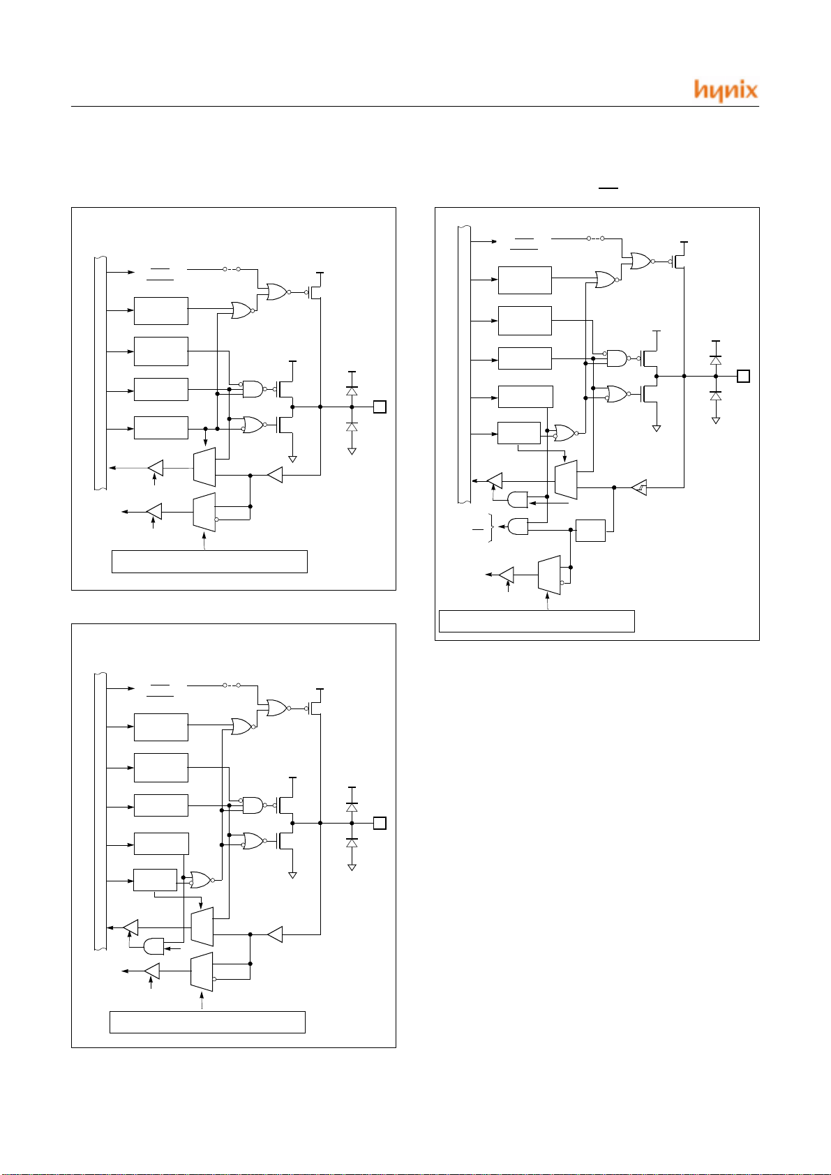
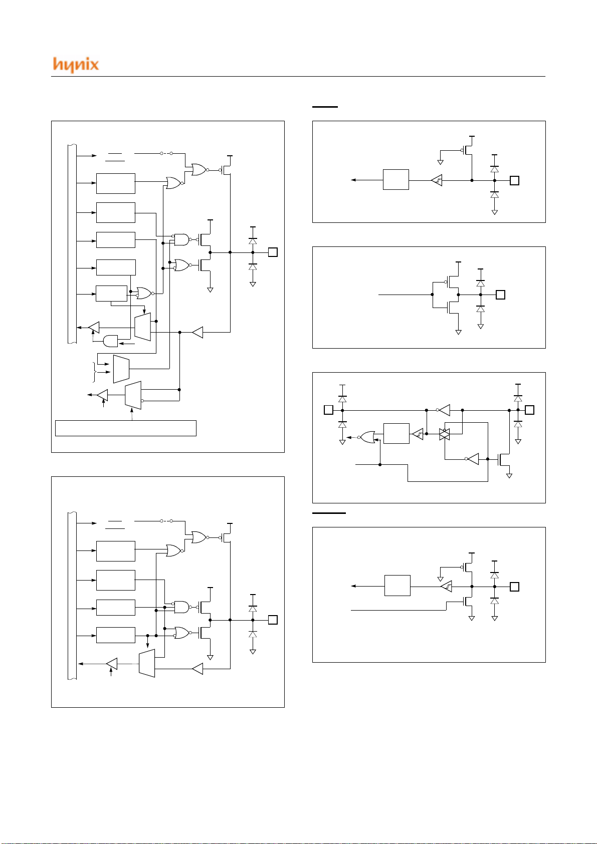
6. PORT STRUCTURES .........................10
7. ELECTRICAL CHARACTERISTICS ...12
Absolute Maximum Ratings .............................12
Recommended Operating Conditions ..............12
DC Electrical Characteristics ............................12
REMOUT Port Ioh Characteristics Graph ........13
REMOUT Port Iol Characteristics Graph .........14
AC Characteristics ...........................................14
8. MEMORY ORGANIZATION ................16
Registers ..........................................................16
Program Memory .............................................19
Data Memory ....................................................22
List for Control Registers.................................. 23
Addressing Mode .............................................25
9. I/O PORTS ..........................................30
R0 Ports........................................................... 30
R1 Ports ...........................................................30
R2 Port .............................................................32
10. CLOCK GENERATOR ......................33
Oscillation Circuit .......................................... 34
11. BASIC INTERVAL TIMER ................36
12. WATCH DOG TIMER .......................38
13. Timer0, Timer1, Timer2 ....................39
14. INTERRUPTS ...................................47
Interrupt priority and sources ........................ 48
Interrupt control register ................................ 48
Interrupt accept mode ................................... 49
Interrupt Sequence ........................................ 50
BRK Interrupt ................................................ 52
Multi Interrupt ................................................ 52
External Interrupt ........................................... 52
Key Scan Input Processing ........................... 53
15.STANDBY FUNCTION ......................55
Sleep Mode.................................................... 55
STOP MODE .................................................. 55
STANDBY MODE RELEASE ......................... 56
RELEASE OPERATION OF STANDBYMODE58
16. RESET FUNCTION ..........................60
EXTERNAL RESET ...................................... 60
POWER ON RESET ..................................... 60
Low Voltage Detection Mode ........................ 62
A. MASK ORDER SHEET ........................i
B. INSTRUCTION ....................................ii
Terminology List ...............................................ii
Instruction Map .................................................iii
Instruction Set ..................................................iv
JUNE 2001 Ver 1.00

HMS81004E/08E/16E/24E/32E
HMS81004E/08E/16E/24E/32E
CMOS SINGLE- CHIP 8-BIT MICROCONTROLLER
FOR UNIVERSAL REMOTE CONTROLLER
1. OVERVIEW
1.1 Description
The HMS81004E/08E/16E/24E/32E is an advanced CMOS 8-bit microcontroller with 4/8/16/24/32K bytes of ROM. The
device is one of GMS800 family. The HYNIX HMS81004 E/08E/16E/24E/32E is a powerfu l microcontroller which provides
a highly flexible and cost effective solution to many UR applications.The HMS81004E/0 8E/16E/24E/32E provides the following standard features: 4/8/16/24/32K bytes of ROM, 448 bytes of RAM, 8-bit timer/counter, on-chip oscillator and clock
circuitry. In addition, the HMS81004E/08E/16E/24E/32E supports power saving modes to reduce power consumption.
Device Name ROM Size EPROM Size RAM Size Package
HMS81004E 4K Bytes HMS81008E 8K Bytes HMS81016E 16K Bytes HMS81024E 24K Bytes -
HMS81032E 32K Bytes HMS81020TL - 20K Bytes
HMS81032TL - 32K Bytes
1.2 Features
• Instruction Cycle Time:
- 1us at 4MHz
• Programmable I/O pins
20 PIN 24 PIN 28 PIN
INPUT 3 3 3
OUTPUT 2 2 2
I/O 13 17 21
• Operating Voltage
- 2.0 ~ 3.6 V @ 4MHz (MASK)
- 2.0 ~ 4.0 V @ 4MHZ (OTP)
•Timer
- Timer / Counter ......... 16Bit * 1ch
......... 8Bit * 2ch
- Basic Interval Timer ...... 8Bit * 1ch
448 Bytes
( included
256 bytes
stack memory )
- Watch Dog Timer ............ 6Bit * 1ch
• 8 Interrupt sources
- Nested Interrupt control is available.
- External input: 2
- Keyscan input
- Basic Interval Timer
- Watchdog timer
- Timer : 3
• Power On Reset
• Power saving Operation Modes
- STOP Operation
- SLEEP Operation
• Low Voltage Detection Circuit
• Watch Dog Timer Auto Start (During 1second
after Power on Reset)
20 SOP/PDIP
24 SOP/Skinny DIP
28 SOP/Skinny DIP
JUNE 2001 Ver 1.00 1

HMS81004E/08E/16E/24E/32E
1.3 Development Tools
The HMS81004E/08E/16E/24E/32E are supported by a full-featured macro assembler, an in-circuit emulator CHOICE-Dr.
and OTP programmers. Macro assembler operates under the MSWindows 95/98
Please contact sales part of HYNIX
TM
/NT4/W2000.
TM
Software
Hardware
(Emulator)
OTP program-
mer
- MS- Window base assembler
- Linker / Editor / Debugger
- CHOICE-Dr.
- CHOICE-Dr. EVA 81C5EVA
- Universal single programmer.
- 4 gang programmer
- stand alone
2 JUNE 2001 Ver 1.00
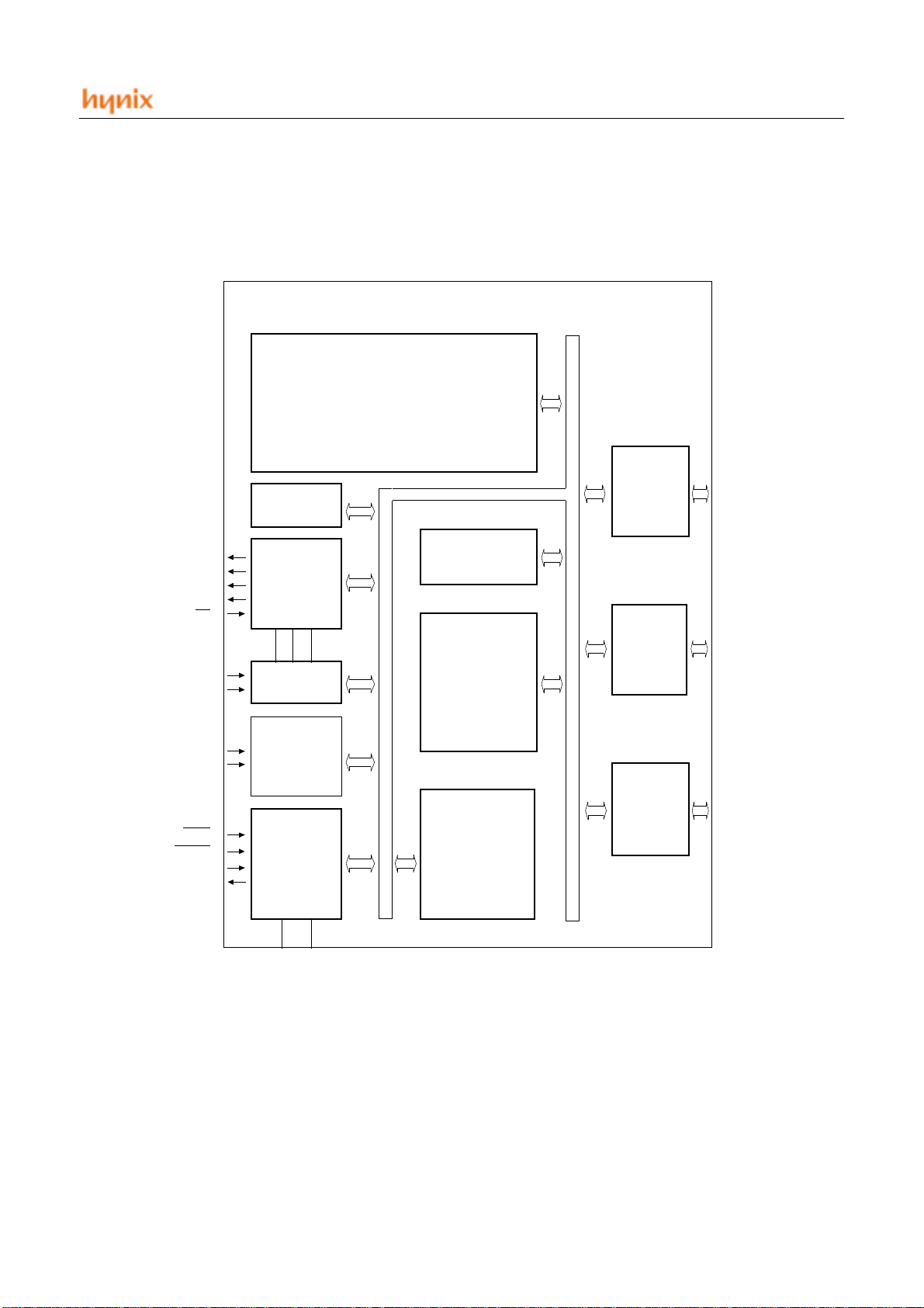
2. BLOCK DIAGRAM
HMS81004E/08E/16E/24E/32E
G8MC
Core
REMOUT
R17/T0
R16/T1
R15/T2
R14/EC
R12/INT2
R11/INT1
R00~R07
R10~R17
TEST
RESET
XIN
XOUT
Watchdog
Timer
Timer
Interrupt
Key Scan
INT.
Generation
Block
Clock Gen.
&
System
Control
RAM
(448byte)
ROM
(32kbyte)
Prescaler
&
B.I.T
R0
PORT
R1
PORT
R2
PORT
R00~R07
R10~R17
R20~R24
VDD VSS
JUNE 2001 Ver 1.00 3

HMS81004E/08E/16E/24E/32E
3. PIN ASSIGNMENT (Top View)
R13
R12
R11
R10
VDD
XOUT
XIN
R00
R01
R02
R03
R20
R21
R22
1
2
3
4
5
6
7
8
9
10
11
12
13
14
28PIN
28
27
26
25
24
23
22
21
20
19
18
17
16
15
R14
R15
R16
R17
REMOUT
RESET
TEST
R07
R06
R05
R04
VSS
R24
R23
R13
R12
R11
R10
VDD
XOUT
XIN
R00
R01
R02
R03
R20
1
2
3
4
5
6
7
8
9
10
11
12
24PIN
24
23
22
21
20
19
18
17
16
15
14
13
R14
R15
R16
R17
REMOUT
RESET
TEST
R07
R06
R05
R04
VSS
R11
R10
VDD
XOUT
XIN
R00
R01
R02
R03
R20
1
2
3
4
5
6
7
8
9
10
20PIN
20
19
18
17
16
15
14
13
12
11
R16
R17
REMOUT
RESET
TEST
R07
R06
R05
R04
VSS
4 JUNE 2001 Ver 1.00
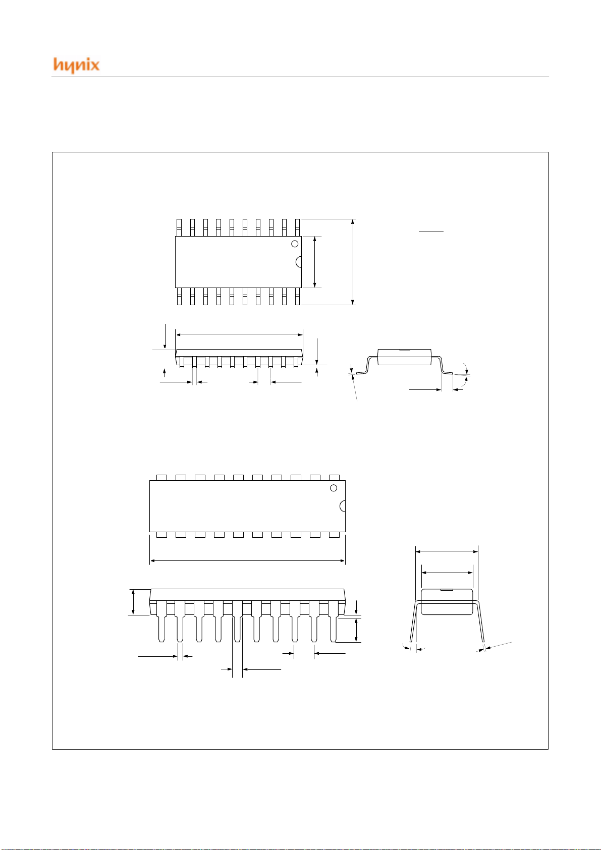
4. PACKAGE DIMENSION
HMS81004E/08E/16E/24E/32E
20 SOP
20 PDIP
0.093
0.105
0.020
0.013
0.512
0.495
0.050 BSC
0.229
0.291
0.012
0.004
0.419
3
1
0
.
0
0.398
8
0
0
.
0
UNIT: INCH
MAX
MIN
0.042
0.016
0 ~ 8°
0 ~ 15°
0.300 BSC
0.270
0.245
012
0.
08
0
0.
MAX 0.180
0.021
0.015
1.043
1.015
0.065
0.050
0.100 BSC
MIN 0.015
0.120
0.140
JUNE 2001 Ver 1.00 5
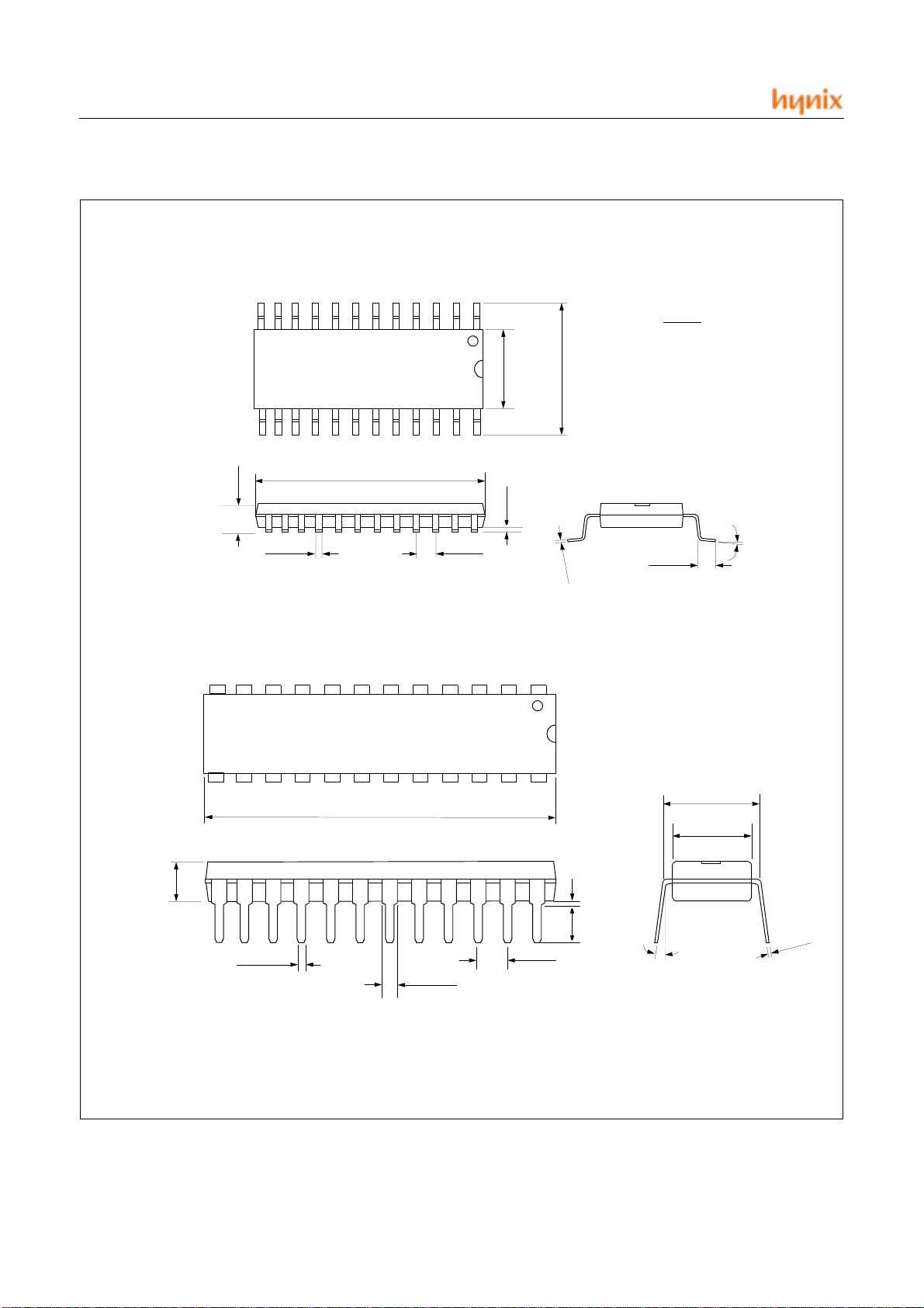
HMS81004E/08E/16E/24E/32E
24 SOP
24 SKDIP
0.093
0.106
0.020
0.013
0.614
0.598
0.050 BSC
0.229
0.291
0.004
0.012
UNIT: INCH
MAX
MIN
0.419
0.398
8
3
0
1
0
.
0
.
0
0
0.042
0.016
0 ~ 8°
0 ~ 15°
0.300 BSC
0.300
0.250
14
0
0.
008
0.
MAX 0.180
0.021
0.015
1.265
1.160
0.065
0.045
0.100 BSC
MIN 0.015
0.120
0.140
6 JUNE 2001 Ver 1.00
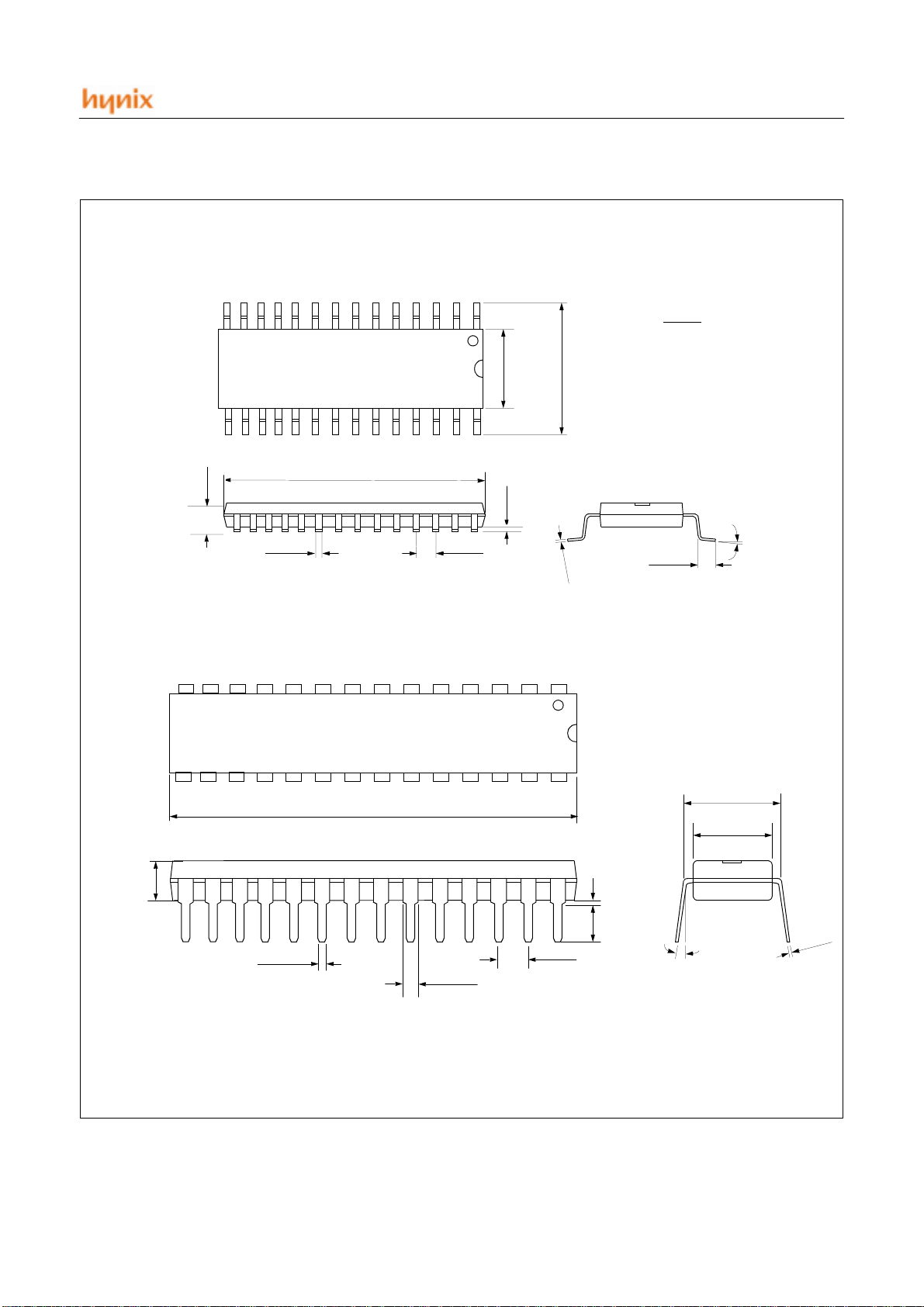
HMS81004E/08E/16E/24E/32E
28 SOP
UNIT: INCH
MAX
MIN
0.229
0.291
0.419
0.398
0.713
0.093
0.106
0.697
0.004
0.012
MAX 0.180
28 SKDIP
0.020
0.013
0.021
0.015
1.375
1.355
0.050 BSC
0.055
0.045
8
3
0
1
0
.
0
.
0
0
0.100 BSC
MIN 0.015
0.120
0.140
0.042
0.016
0 ~ 15°
0 ~ 8°
0.300 BSC
0.300
0.275
14
0
0.
008
0.
JUNE 2001 Ver 1.00 7

HMS81004E/08E/16E/24E/32E
5. PIN FUNCTION
V
: Supply voltage.
DD
V
: Circuit ground.
SS
TEST
: Used for shipping inspection of the IC. For normal
operation, it should be connected to V
RESET
X
: Reset the MCU.
: Input to the inverting oscillator amplifier and input to
IN
DD
.
the internal main clock operating circuit.
X
: Output from the inverting oscillator amplifier.
OUT
R00~R07
: R0 is an 8-bit CMOS bidirectional I/O port. R0
pins 1 or 0 written to the Port Direction Register can be
used as output s or inputs.
R10~R17
: R1 is an 8-bit CMOS bidirectional I/O port. R1
pins 1 or 0 written to the Port Direction Register can be
used as outputs or inputs.
In addition, R1 serves the functions of the various follow -
ing special features .
Port pin Alternate function
R11
R12
R14
R15
R16
R17
R20~R24
INT1 (External Interrupt input 1)
INT2 (External Interrupt input 2)
EC
T2 (Timer / Counter input 2)
T1 (Timer / Counter input 1)
T0 (Timer / Counter input 0)
: R2 is an 8-bit CMOS bidirectional I/O port. R2
(Event Counter input )
pins 1 or 0 written to the Port Direction Register can be
used as outputs or inputs .
8 JUNE 2001 Ver 1.00

HMS81004E/08E/16E/24E/32E
PIN NAME
R00 I/O
R01 I/O
R02 I/O
R03 I/O
R04 I/O
R05 I/O
R06 I/O
R07 I/O
R10 I/O
R11/INT1 I/O
R12/INT2 I/O
R13 I/O
R14/EC
R15/T2 I/O
R16/T1 I/O
R17/T0 I/O
R20 I/O - Each bit of the port can be individually configured as
R21 I/O
R22 I/O
R23 I/O
R24 I/O
XIN I Oscillator input Low
XOUT O Oscillator output High
REMOUT O High current output ‘L’ output ‘L’ output
RESET
TEST
VDD P Positive power supply
VSS P Groud
INPUT/
OUTPUT
- Each bit of the port can be individually configured as
an input or an output by user software
- Push-pull output
- CMOS input with pull-up resister (option)
- Can be programmable as key scan input
- Pull-up resisters are automatically disabled at output
mode
- Each bit of the port can be individually configured as
an input or an output by user software
- Push-pull output
- CMOS input with pull-up resister (option)
I/O
I Includes pull-up resistor ‘L’ level
I Includes pull-up resistor
- Can be programmable as key scan input or open
drain output
- Pull-up resisters are automatically disabled at output
mode
- Direct driving of LED(N-Tr.)
an input or an output by user software
- Push-pull output
- CMOS input with pull-up resister (option)
- Pull-up resisters are automatically disabled at output
mode
- Direct driving of LED(N-Tr.)
Function @RESET @STOP
INPUT
INPUT
INPUT
State of
before
Stop
State of
before
Stop
State of
before
Stop
state of
before stop
JUNE 2001 Ver 1.00 9
HMS81004E/08E/16E/24E/32E
Pin
Data Reg.
Function Sele-
Key Scan
Pull up
Reg.
Rd
V
DD
V
SS
Pull-up Tr.
Input
Open Drain
Reg.
Data Bus
Tr.: Transistor
Reg.: Register
LVD
Circuit
OTP : connected
MASK : option (default connected)
V
DD
KS_EN
Standby Release Level Control Regist er
ction Reg.
Dir Reg.
MUX
Noise
Filter
to R11...INT1
to R12...INT2
to R14...EC
MUX
6. PORT STRUCTURES
R0[0:7]
Data Bus
Key Scan
Input
OTP : connected
LVD
Circuit
Pull up
Reg.
Open Drain
Reg.
Data Reg.
Dir. Reg.
Rd
KS_EN
Standby Release Level Control Register
MASK : option (default connected)
V
DD
V
SS
MUX
MUX
V
DD
Pull-up Tr.
Tr.: Transistor
Reg.: Register
R11/INT1, R12/INT2, R14/EC
Pin
R10, R13
Data Bus
Key Scan
Input
OTP : connected
LVD
Circuit
Pull up
Reg.
Open Drain
Reg.
Data Reg.
Function Selection Reg.
Dir Reg.
KS_EN
Standby Release Level Control Register
MASK : option (default connected)
V
DD
Rd
MUX
MUX
V
SS
V
DD
Pull-up Tr.
Tr.: Transistor
Reg.: Register
Pin
10 JUNE 2001 Ver 1.00
HMS81004E/08E/16E/24E/32E
Pin
V
DD
V
SS
Noise
Filter
Pin
V
DD
V
SS
Internal Signal
XIN
V
SS
XOUT
Noise
Filter
from STOP circuit
Pin
V
DD
V
SS
Noise
Filter
from Power On Reset
R15/T2, R16/T1, R17/T0
OTP : connected
LVD
Circuit
Pull up
Reg.
Open Drain
Reg.
Data Reg.
Data Bus
Function Selection Reg.
Dir Reg.
to R15...T2
to R16...T1
to R17...T0
Key Scan
Input
Standby Release Level Control Register
KS_EN
MASK : option (default connected)
MUX
Rd
MUX
MUX
TEST
V
DD
Pull-up Tr.
V
DD
REMOUT
Pin
V
SS
XIN, XOUT
Tr.: Transistor
Reg.: Register
R2[0:4]
OTP : connected
LVD
Circuit
Pull up
Reg.
Open Drain
Reg.
Data Reg.
Data Bus
Dir. Reg.
Rd
JUNE 2001 Ver 1.00 11
MASK : option (default connected)
MUX
V
DD
Pull-up Tr.
V
DD
Pin
V
SS
Tr.: Transistor
Reg.: Register
RESET

HMS81004E/08E/16E/24E/32E
7. ELECTRICAL CHARACTERISTICS
7.1 Absolute Maximum Ratings
Supply voltage...........................................-0.3 to +5.0 V
Input Voltage .....................................-0.3 to V
Output Voltage ...................................-0.3 to V
DD
DD
+0.3 V
+0.3 V
Operating Temperature........................................ 0~70°C
Storage Temperature ......................................-65~150°C
Power Dissipation................................................700 mA
7.2 Recommended Operating Conditions
Parameter Symbol Condition
Supply Voltage
Operating Frequency
Operating Temperature
V
T
DD
f
XIN
OPR
f
XIN
VDD=2.0~3.6V
7.3 DC Electrical Characteristics
(TA=-0~70°C, VDD=2.0~3.6V, GND=0V)
Parameter Symbol Condition
Note: Stresses above those listed under “Absolute Maxi-
mum Ratings” may cause per manent damage to the d evice. This is a stress ra ting only and functional ope r ati on of
the device at any oth er c ond iti ons ab ov e tho se ind ic ated in
the oper ati o na l se c ti ons of this s pe c ifi ca t io n i s no t i m pl ie d .
Exposure to absolute maximum rating conditions for extended periods may affect device reliability.
Specifications
Unit
Min. Max.
=4MHz
2.0 3.6 V
1.0 4.0 MHz
-0+70
°
C
Specifications
Unit
Min. Typ. Max.
High level
input Voltage
Low level
input Voltage
Hign level input
Leakage Current
Low level input
Leakage Current
High level
output Voltage
Low level
output Voltage
Hign level output
Leakage Current
Low level output
Leakage Current
V
V
V
V
V
V
V
V
V
V
I
I
IH1
IH2
IL1
IL2
I
IH
I
IL
OH1
OH2
OH3
OL1
OL2
OL3
OHL
OLL
R11,R12,R14,RESET
R0,R1(except R11,R12,R14), R2
R11,R12,R14,RESET 0R0,R1(except R11,R12,R14), R2 0 -
R0,R1,R2,RESET ,VIH= VDD
R0,R1,R2,RESET (without pu ll-up),VIL= 0
R0, IOH=-0.5mA
R1[6:0], R2, IOH=-1.0mA
XIN, XOUT,IOH=-200µA
R0, IOL=1mA
R1, R2, IOL=5mA
XIN, XOUT,IOL=200µA
R0,R1,R2, VOH= VDD
R0,R1,R2, VOL= 0
0.8 V
0.7 V
DD
DD
-
-
0.2 V
0.3 V
--1µA
---1µA
VDD-0.4 - - V
VDD-0.4 - - V
VDD-0.9 - - V
--0.4V
--0.8V
--0.8V
--1µA
---1µA
V
DD
V
DD
DD
DD
V
V
V
V
12 JUNE 2001 Ver 1.00
HMS81004E/08E/16E/24E/32E
Parameter Symbol Condition
High Level
output current
Low Level
output cruuent
Input pul l-up curren t
Power Supply Current
RAM retention
supply voltage
I
OH
I
OL
I
I
DD1
I
DD2
I
SLP1
I
SLP2
I
STP1
I
STP2
V
RET
REMOUT, R17, V
REMOUT, V
R0,R1,R2, RESET, VDD=3V 15 30 60
p
Operating current ,fxin=4Mhz, VDD=2.0V - 2.4 6 mA
Operating current ,fxin=4Mhz, VDD=3.6V - 4 10 mA
Sleep mode current ,fxin=4Mhz,
VDD=2.0V
Sleep mode current ,fxin=4Mhz,
VDD=3.6V
Stop mode current ,Oscillator Stop
VDD=2.0V
Stop mode current ,Oscillator Stop
VDD=3.6V
OL
Specifications
Unit
Min. Typ. Max.
=2V -30
OH
=1V
0.5 - 3 mA
-12 -5 mA
µ
A
-12mA
-23mA
-28µA
-310µA
-0.7--V
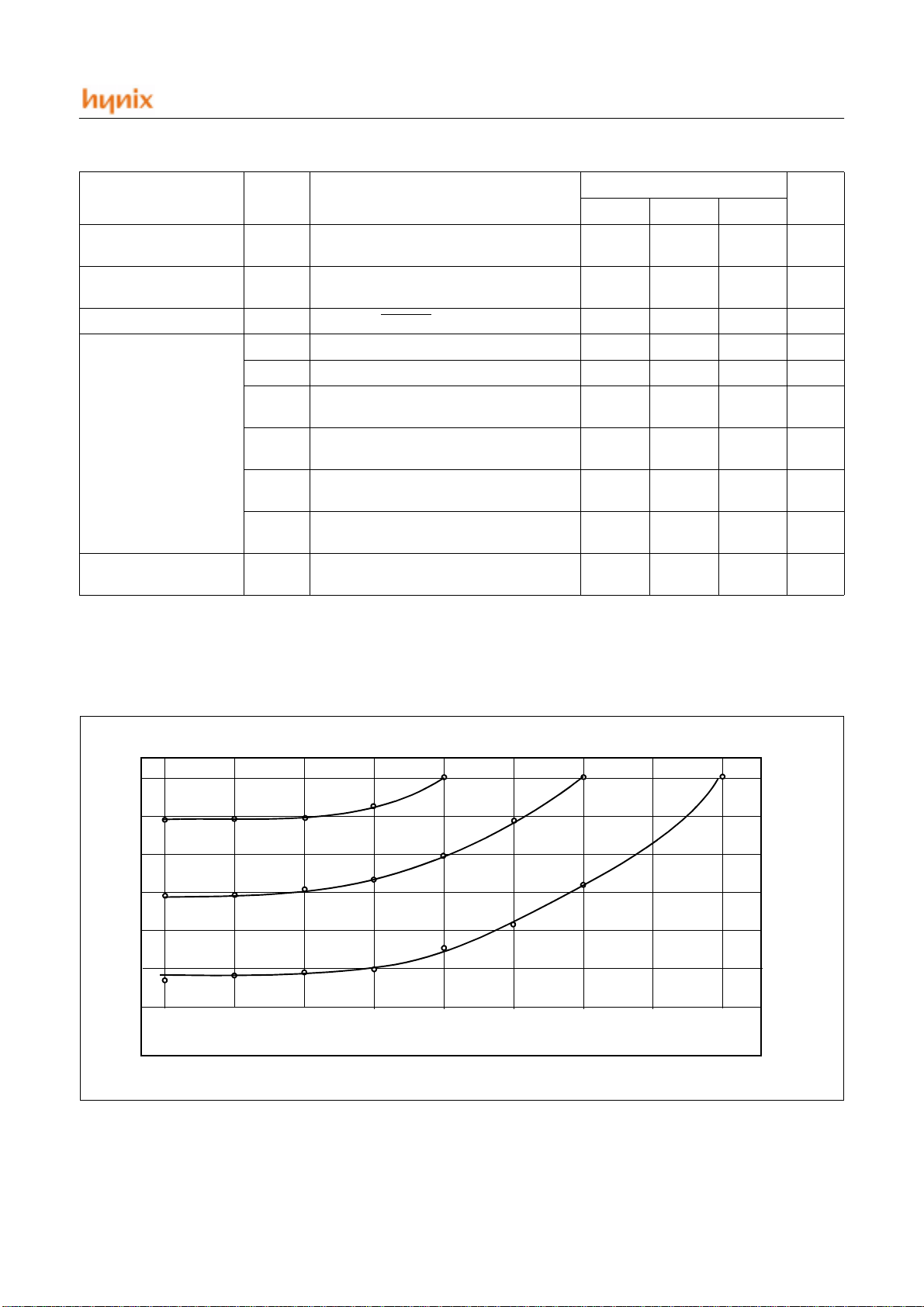
7.4 REMOUT Port Ioh Characteristics Graph
(typical process & room temperature)
.
Ioh(mA)
0
-5
-10
-15
-20
-25
-30
0 0.5 1.0 1.5 2.0 2.5 3.0 3.5 4.0
Voh (
Vdd 2V
Vdd 3V
Vdd 4V
V)
Figure 7-1 Ioh vs Voh
JUNE 2001 Ver 1.00 13
HMS81004E/08E/16E/24E/32E
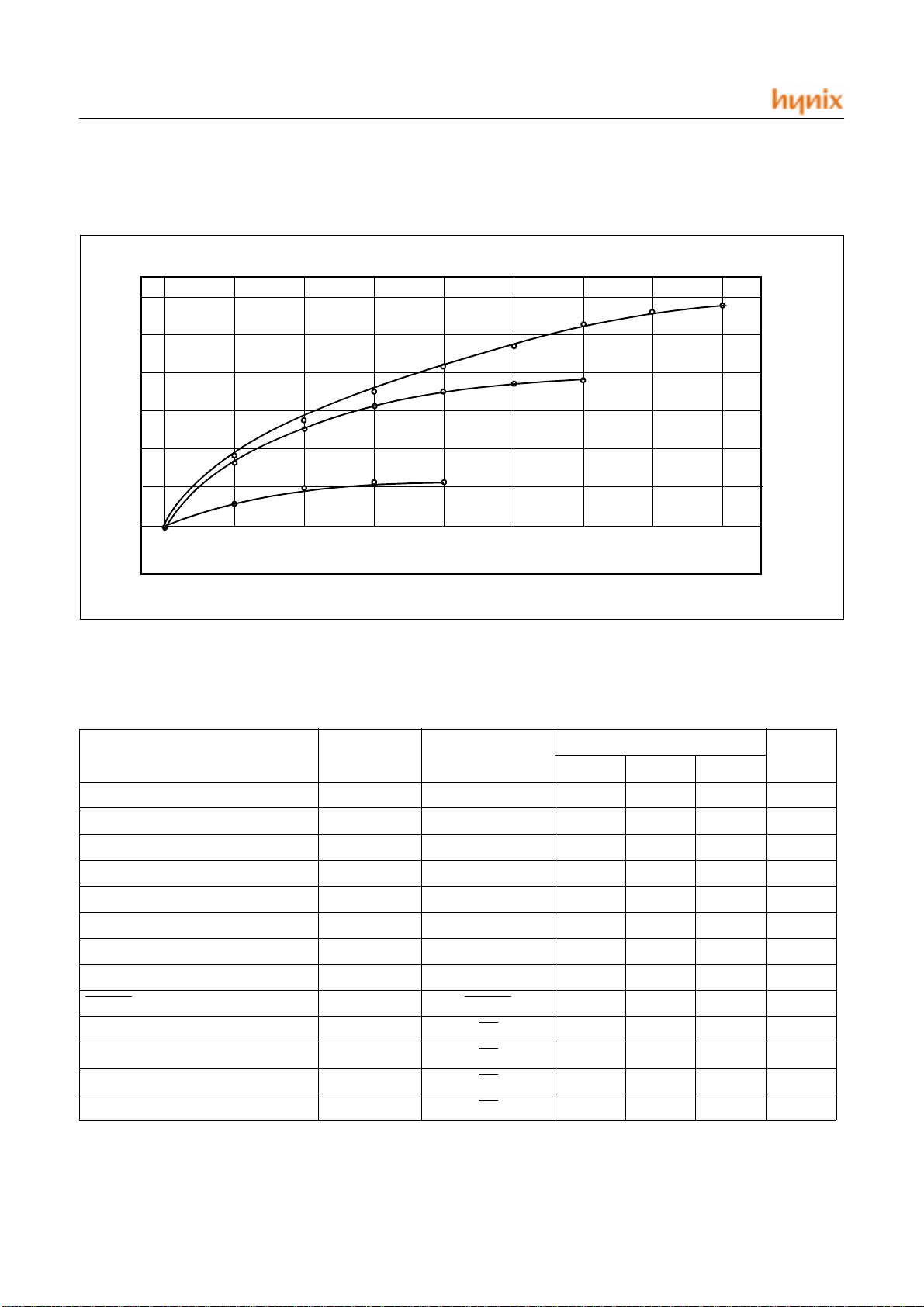
7.5 REMOUT Port Iol Characteristics Graph
(typical process & room temperature)
.
Iol(mA)
5
4
3
2
1
0
-1
0 0.5 1.0 1.5 2.0 2.5 3.0 3.5 4.0
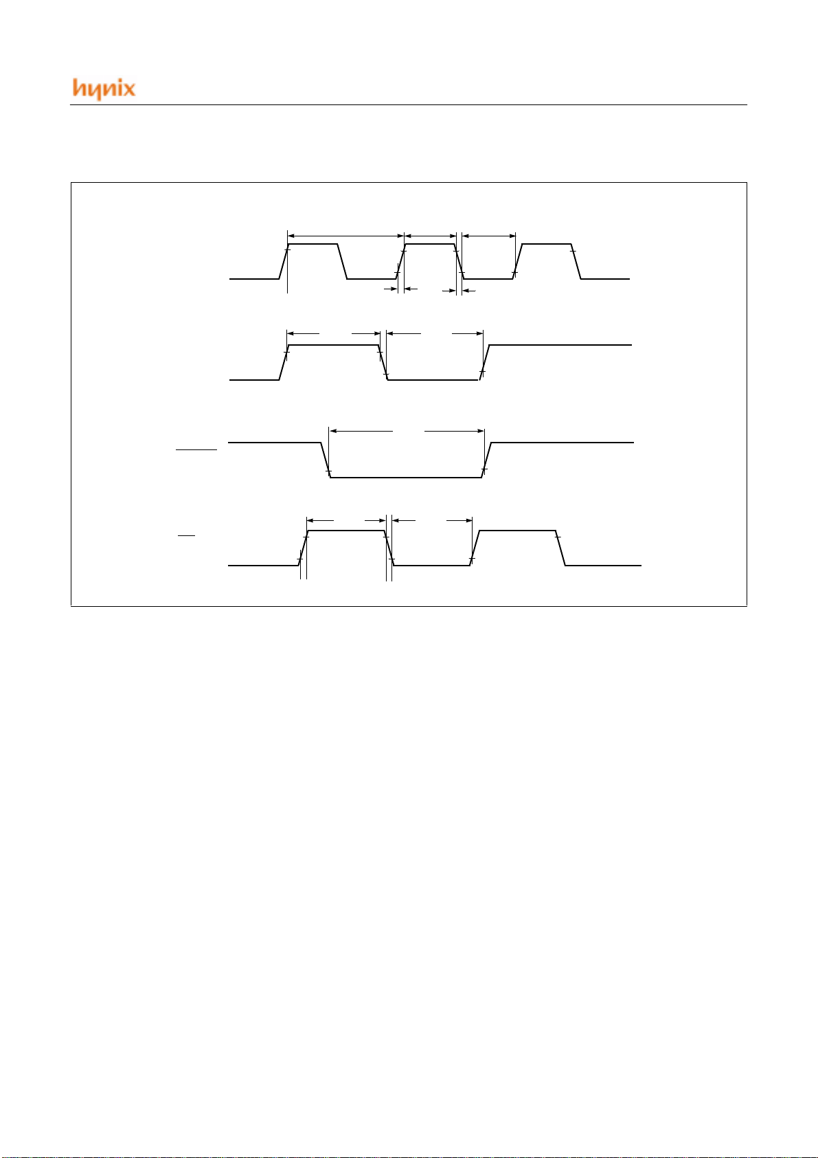
7.6 AC Characteristics
(TA=0~+70°°°°C, VDD=2.0~3.6V, VSS=0V)
Parameter Symbol Pins
Vdd 2V
Vol (
V)
Figure 7-2 Iol vs Vol
Vdd 4V
Vdd 3V
Specifications
Unit
Min. Typ. Max.
External clock input cycle time
System clock cycle time
External clock pulse width High
External clock pulse width Low
External clock rising time
External clock falling time
Interrupt pulse width High
Interrupt pulse width Low
RESET Input pulse width low
Event counter input pulse width high
Event counter input pulse width low
Event counter input pulse rising time
Event counter input pu lse fa lling time
t
CP
t
SYS
t
CPH
t
CPL
t
RCP
t
FCP
t
t
t
RSTL
t
ECH
t
ECL
t
REC
t
FEC
IH
IL
X
IN
250 500 1000 ns
500 1000 2000
X
IN
X
IN
X
IN
X
IN
40 - - ns
40 - - ns
- - 40 ns
- - 40 nS
INT1, INT2 2 - INT1, INT2 2 - -
RESET 8--
EC 2-EC 2-EC --40
EC --40
t
SYS
t
SYS
t
SYS
t
SYS
t
SYS
ns
ns
ns
14 JUNE 2001 Ver 1.00
HMS81004E/08E/16E/24E/32E
X
IN
INT1
INT2
RESET
EC
t
CP
t
RCP
t
IH
0.8V
DD
t
RSTL
t
ECH
Figure 7-3 Timing Diagram
t
CPH
t
ECL
t
CPL
-0.5V
V
DD
0.5V
t
FCP
t
IL
0.2V
DD
0.2V
DD
0.8V
DD
0.2V
DD
JUNE 2001 Ver 1.00 15

HMS81004E/08E/16E/24E/32E
8. MEMORY ORGANIZATION
The HMS81004E/08E/16E/24E/32E has separate address
spaces for Program memory and Data Memory. Program
memory can only be read, not written to. It can be up to
8.1 Registers
This device has six registers that are the Program Counter
(PC), an Accumulator (A), two index registers (X, Y), the
Stack Pointer (SP), and the Program Status Word (PSW).
The Program Counter consists of 16-bit register.
A
X
Y
SP
PCLPCH
PSW
Figure 8-1 Configuration of Registers
Accumulator:
The Accumulator is the 8-bit general purpose register, used
for data operation such as transfer, temporary saving, and
conditional judgement, etc. The Accumulator can be used
as a 16-bit register with Y Register as shown below.
In the case of multiplication instruction, execute as a multiplier register. After multiplication operation, the lower 8bit of the result enters. (Y*A => YA). In the case of division instruction, ex ecute as the lo wer 8-bit of di vidend. After division operation, quotient enters.
Y
A
Two 8-bit Registers can be used as a "YA" 16-bit Register
ACCUMULATOR
X REGISTER
Y REGISTER
STACK POINTER
PROGRAM COUNTER
PROGRAM STATUS
WORD
Y A
32K bytes of Program memory. Data memory can be read
and written to up to 448 bytes including the stack area.
X, Y Registers:
In the addressing mode which uses these index registers,
the register contents are added to the specified address,
which becomes the actual address. These modes are extremely effective for referencing subroutine tables and
memory tables. The index registers also have increment,
decrement, comparison and data transfer functions, and
they can be used as simple accumulators.
• X Regist er
In the case of division instruction, execute as register.
• Y Regist er
In the case of 16-bit operation instruction, execute as the
upper 8-bit of YA. (16-bit accumulator). In the case of
multiplication instruction, execute as a multiplicand register. After multiplication operation, the upper 8-bit of the
result enters. In the case of division instruction, execute as
the upper 8-bit of dividend. After division operation, remains enters. Y register can be used as loop counter of
conditional branch command. (e.g.DBNE Y, rel)
Stack Pointer:
The Stack Pointer is an 8-bit register used for occurrence
interrupts, calling out subroutines and P USH, POP, RETI,
RET instruction. Stack Pointer identifies the location in the
stack to be accessed (save or restore).
Generally, SP is automatically updated when a subrout ine
call is executed or an interrupt is accepted. However, if it
is used in excess of the stack area permitted by the data
memory allocating configuration, the user-processed data
may be lost. The SP is post-decremented when a subroutine call or a push instruction is executed, or when an interrupt is accepted. The SP is pre-incremented when a return
or a pop instruction is executed.
Figure 8-2 Configuration of YA 16-bit Register
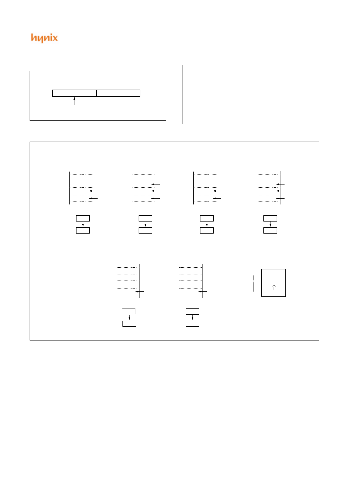
The stack can be located at any position within 100
1FF
of the internal data memory. The SP is not initialized
H
to
H
by hardware, requiring to write the initial v alue (the lo cation with which the use of the stack starts) by using the initialization routine. Normally, the initial value of "FF
H
" is
16 JUNE 2001 Ver 1.00
HMS81004E/08E/16E/24E/32E
used.
Stack Address ( 100H ~ 1FFH )
15 087
01
H
Hardware fixed
At execution of
a CALL/TCALL/PCALL
01FC
01FD
01FE
01FF
SP before
execution
SP after
execution
PCL
PCH
01FF
01FD
Push
down
SP
01FC
01FD
01FE
01FF
At acceptance
of interrupt
PSW
PCL
PCH
01FF
01FC
Push
down
Caution:
The Stack Pointer must be initialized by software be-
cause its value is undefined after RESET.
Example: To initialize the SP
LDX #0FFH
TXSP ; SP ← FFH
At execution
of RET instruction
01FC
01FD
01FE
01FF
PCL
PCH
01FD
01FF
Pop
up
At execution
of RETI instruction
01FC
01FD
01FE
01FF
PSW
PCL
PCH
01FC
01FF
Pop
up
At execution
of PUSH instruction
PUSH A (X,Y,PSW)
01FC
01FD
SP before
execution
SP after
execution
01FE
01FF
01FF
01FE
Push
A
down
Figure 8-3 Stack Operation
Program Counter:
The Program Counter is a 16-bit wide which consists of
two 8-bit registers, PCH and PCL. This counter indicates
the address of the next instruction to be executed. In reset
state, the program counter has reset routine address
(PC
:0FFH, PCL:0FEH).
H
Program Status Word:
The Program Status Word (PSW) contains several bits that
At execution
of POP instruction
POP A (X,Y,PSW)
01FC
01FD
01FE
01FF
A
01FE
01FF
Pop
up
0100H
01FFH
Stack
depth
reflect the current state of the CPU. The PSW is described
in Figure 8-4 . It contains the Negative flag, the Overflow
flag, the Break flag the Half Carry (for BCD operation),
the Interrupt enable flag, the Zero flag, and the Carry flag.
[Carry flag C]
This flag stores any carry or borrow from the ALU of CPU
after an arithmetic operation and is also changed by the
Shift Instruction or Rotate Instruction.
JUNE 2001 Ver 1.00 17

HMS81004E/08E/16E/24E/32E
[Zero flag Z]
This flag is set when the result of an arithmetic operat ion
or data transfer is "0" and is cleared by any other result.
MSB LSB
N
PSW
V G B H I Z C
RESET VALUE : 00
H
NEGATIVE FLAG
OVERFLOW FLAG
SELECT DIRECT PAGE
when g=1, page is addressed by RPR
BRK FLAG
Figure 8-4 PSW (Program Status Word) Register
[Interrupt disable flag I]
This flag enables/disables all interrupts except interrupt
caused by Reset or software BRK instruction. All interrupts are disabled when cleared to "0". This flag immediately becomes "0" when an interrupt is served. It is set by
the EI instruction and cleared by the DI instruction.
[Half carry flag H]
After operation, this is set when there is a carry from bit 3
of ALU or there is no borrow from bit 4 of ALU. This bit
can not be set or cleared except CLRV instruction with
Overflow flag (V).
[Break flag B]
This flag is set by software BRK instruction to distinguish
BRK from TCALL instruction with the same vector address.
[Direct page flag G]
CARRY FLAG RECEIVES
CARRY OUT
ZERO FLAG
INTERRUPT ENABLE FLAG
HALF CARRY FLAG RECEIVES
CARRY OUT FROM BIT 1 OF
ADDITION OPERLANDS
the direct addressing mode, addressing area is from zero
page 00
to 0FFH when this flag is "0". If it is set to "1",
H
addressing area is 1 Page. It is set by SETG instruction and
cleared by CLRG.
[Overflow flag V]
This flag is set to "1" when an overflow occurs as the result
of an arithmetic operation involving signs. An overflow
occurs when the result of an addition or subtraction exceeds +127(7F
) or -128(80H). The CLRV instruction
H
clears the overflow flag. There is no set instruction. When
the BIT instruction is executed, bit 6 of memory is copied
to this flag.
[Negative flag N]
This flag is set to match the sign bit (bit 7) status of the result of a data or arithmetic operation. When the BIT instruction is executed, bit 7 of memory is copied to this flag.
This flag assigns RAM page for di rect addressing mode. I n
18 JUNE 2001 Ver 1.00

8.2 Program Memory
E0
E2
Address
Vector Area Memory
E4
E6
E8
EA
EC
EE
F0
F2
F4
F6
F8
FA
FC
FE
-
-
-
Basic Interval Timer Interrupt Vector Area
-
-
Timer2 Interrupt Vector Area
Timer0 Interrupt Vector Area
-
External Interrupt 2 Vector Area
Key Scan Interrupt Vector Area
RESET Vector Area
External Interrupt 1 Vector Area
Timer1 Interrupt Vector Area
Watch Dog Timer Interrupt Vector Area
"-" means reserved area.
NOTE:
-
0FFDE
H
S/W Interrupt Vector Area
HMS81004E/08E/16E/24E/32E
A 16-bit program counter is capable of addressing up to
64K bytes, but this device has 4/8/16/24/32K bytes program memory space only physically implemented. Accessing a location above FFFF
to 0000
.
H
will cause a wrap-around
H
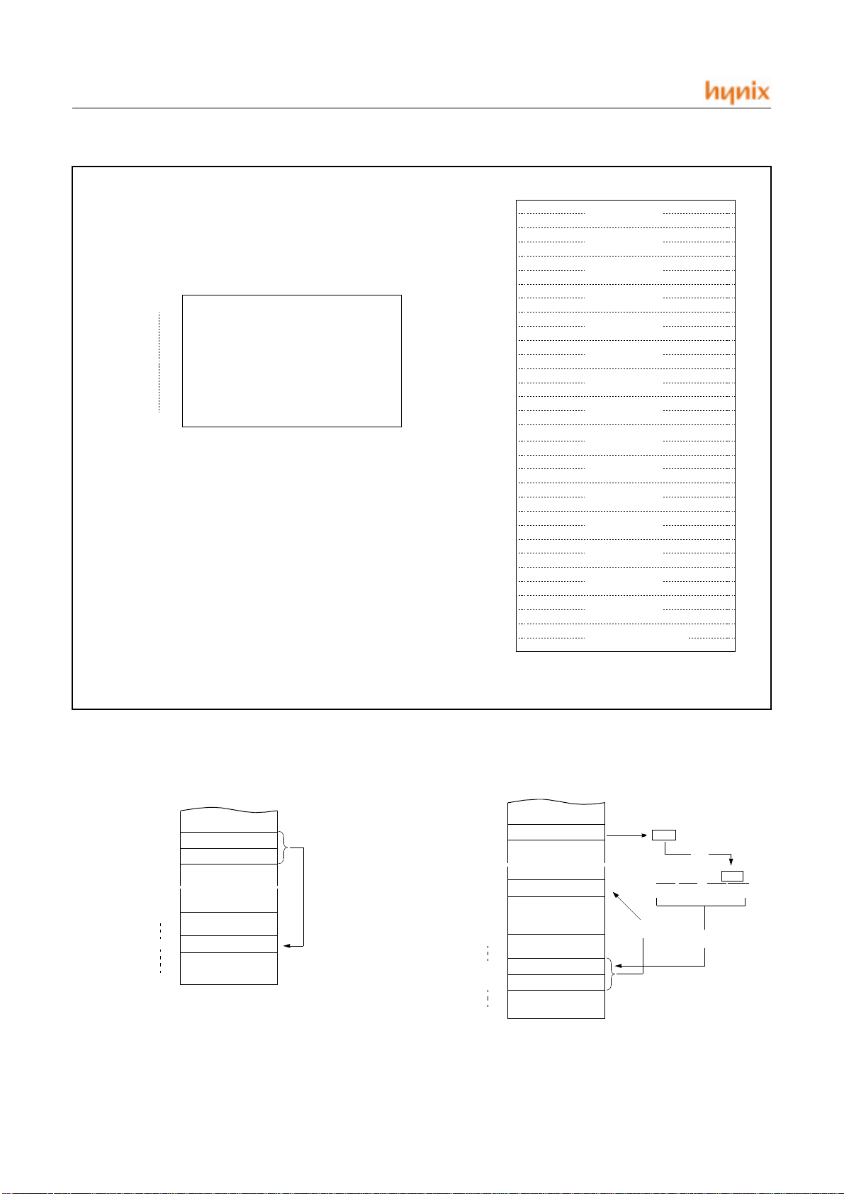
Figure 8-5 , shows a map of Progr am Memory. After reset,
the CPU begins execution from reset vector which is stored
in address FFFE
and FFFFH as shown in Figure 8-6 .
H
As shown in Figure 8-5 , each area is assigned a fixed location in Program M emory. Program Memory area contains the user program.
8000
H
A000
H
C000
H
32KROM
E000
F000
FF00
FFC0
FFE0
FFFF
H
H
H
H
H
INTERRUPT
VECTOR AREA
H
PCALL
AREA
TCALL
AREA
8KROM
4KROM
HMS81008E
HMS81004E
KROM
HMS81016E 16
24KROM
HMS81032E
HMS81024E
Example: Usage of TCALL
LDA #5
TCALL 0FH ;
:;
:;
;
;TABLE CALL ROUTINE
;
FUNC_A: LDA LRG0
RET
;
FUNC_B: LDA LRG1
RET
;
;TABLE CALL ADD. AREA
;
ORG 0FFC0H ;
DW FUNC_A
DW FUNC_B
1BYTE INSTRUCTION
IN STEAD OF 2 BYTES
NORMAL CALL
1
2
TCALL ADDRESS AREA
The interrupt causes the CPU to jum p to specific location,
where it commences the execution of the service routine.
The External interrupt 0, for example, is assigned to location 0FFFA
interval: 0FFF8
0FFFA
Any area from 0FF00
. The interrupt service locations spaces 2-byte
H
and 0FFF9H for External Interru pt 1,
H
and 0FFFBH for External Interrupt 0, etc.
H
to 0FFFFH, if it is not going to be
H
used, its service location is available as general purpose
Program Memory.
Figure 8-5 Program Memory Map
Page Call (PCALL) area contains subroutine program to
reduce program byte length by using 2 bytes PCALL instead of 3 bytes CALL instruction. If it is frequently
called, it is more useful to save program byte length.
Table Call (TCALL) c auses the CPU to jump to each
TCALL address, where it commences the execution of the
service routine. The Table Call service area spaces 2-byte
for every TCALL: 0FFC0
TCALL14, etc., as shown in Figure 8-7 .
JUNE 2001 Ver 1.00 19
for TCALL15, 0FFC2H for
H
Figure 8-6 Interrupt Vector Area
HMS81004E/08E/16E/24E/32E
11111111
11010110
01001010
PC:
FHFHDH6
H
4A
~
~
~
~
25
0FFD6H
0FF00H
0FFFFH
D1
NEXT
0FFD7H
➊
➋
➌
0D125H
Reverse
Address PCALL Area Memory
0FF00
H
PCALL Area
(192 Bytes)
0FFBF
H
Address Pro gram Memory
0FFC0
H
C1
C2
C3
C4
C5
C6
C7
C8
C9
CA
CB
CC
CD
CE
CF
D0
D1
D2
D3
D4
D5
D6
D7
D8
D9
DA
DB
DC
DD
DE
DF
NOTE:
* means that the BRK software interrupt is using
same address with TCALL0.
TCALL 15
TCALL 14
TCALL 13
TCALL 12
TCALL 11
TCALL 10
TCALL 9
TCALL 8
TCALL 7
TCALL 6
TCALL 5
TCALL 4
TCALL 3
TCALL 2
TCALL 1
TCALL 0 / BRK *
Figure 8-7 PCALL and TCALL Memory Area
PCALL
4F35 PCALL 35H
20 JUNE 2001 Ver 1.00
→
→
→ →
rel
0FF00H
0FF35H
0FFFFH
TCALL
→
→
→ →
n
4A TCALL 4
4F
35
~
~
NEXT
~
~

HMS81004E/08E/16E/24E/32E
Example: The usage software example of Vector address and the initialize part.
ORG 0FFE0H
DW NOT_USED
DW NOT_USED
DW NOT_USED
DW B IT_INT ; BIT
DW WDT_INT ; Watch Dog Timer
DW NOT_USED
DW NOT_USED
DW T MR2_INT ; Timer-2
DW T MR1_INT ; Timer-1
DW T MR0_INT ; Timer-0
DW N OT_USED ;
DW I NT2 ; Int.2
DW I NT1 ; Int.1
DW K EY_INT ; Key Scan
DW N OT_USED ;
DW R ESET ; Reset
ORG 08000H ;HMS81032E Program start address
;********************************************
; MAIN PROGRAM *
;********************************************
;
RESET: NOP
RAM_CLR: LDA #0 ;RAM Clear(!0000H->!00BFH)
CLRG
DI ;Disable All Interrupts
LDX #0
STA {X}+
CMPX #0C0H
BNE RAM_CLR ;
LDX #0FFH ;Stack Pointer Initialize
TXSP
LDM R0, #0 ;Normal Port 0
LDM R0DD,#1000_0010B ;Normal Port Direction
LDM P0PC,#1000_0010B ;Pull Up Selection Set
LDM PMR1,#0000_0010B ;R1 port / int
:
:
LDM CKCTLR,#0011_1101B ;WDT ON , 16mS Time delay after stop mode release
:
:
JUNE 2001 Ver 1.00 21
 Loading...