HYNIX GMS90L320Q, GMS90L320PL, GMS90L320, GMS90C320Q50, GMS90C320Q40 Datasheet
...
HYNIX SEMICONDUCTOR INC.
8-BIT SINGLE-CHIP MICROCONTROLLERS
GMS90C320
User’s Manual (Ver. 1.2)

REVISION HISTORY
VERSION 1.2 (Oct. 2000) This book
Correct the pin number of 44-MQFP package type on page 6.
VERSION 1.1 (Oct. 1999) Before version
Version 1.2
Published by
MCU Application Team
Copy right 2001 Hynix semiconductor, All right reserved.
Additional information of this manual may be served by Hynix semiconductor offices in Korea or Distributors and Representatives listed at address directory.
Hynix semiconductor reserves the right to make changes to any information here in at any time without notice.
The information, diagrams and other data in this manual are correct and reliable; however, Hynix semiconductor is in no
way responsible for any violations of patents or other rights of the third party generated by the use of this manual.

GMS90C320
Device Naming Structure
H(G)MS90X320
MCU Series
Hynix semiconductor MCU
XXXX
Frequency
Blank: 24MHz
40: 40MHz
50: 50MHz
Package Type
Blank:
PL:
Q:
Enhanced ROM-less version
Operating Voltage
C:L:Normal voltage
40PDIP
44PLCC
44MQFP
Low voltage
OCT. 2000 Ver 1.2

GMS90C320
GMS90C320 ordering information
Operating
Voltage (V)
4.25~5.5
2.7~5.5
Device Name
GMS90C320 40
GMS90C320 PL40
GMS90C320 Q40
GMS90C320 50
GMS90C320 PL50
GMS90C320 Q50
GMS90L320
GMS90L320 PL
GMS90L320 Q
ROM size
(bytes)
ROM-less 256 40
ROM-less 256 50
ROM-less 256 24
RAM size
(bytes)
Operating max.
Frequency (MHz)
Package Type
40PDIP
44PLCC
44MQFP
40PDIP
44PLCC
44MQFP
40PDIP
44PLCC
44MQFP
OCT. 2000 Ver 1.2

GMS90C320/L320
CMOS SINGLE-CHIP 8-BIT MICROCONT ROLLER
ROM-less Version for 90C52
GMS90C320
Operating Voltage (V) Device Name ROM RAM
4.25~5.5 GMS90C320 ROM-less 256 ×××× 8bit 40/50
2.7~5.5 GMS90L320 ROM-less 256 ×××× 8bit 24
Features
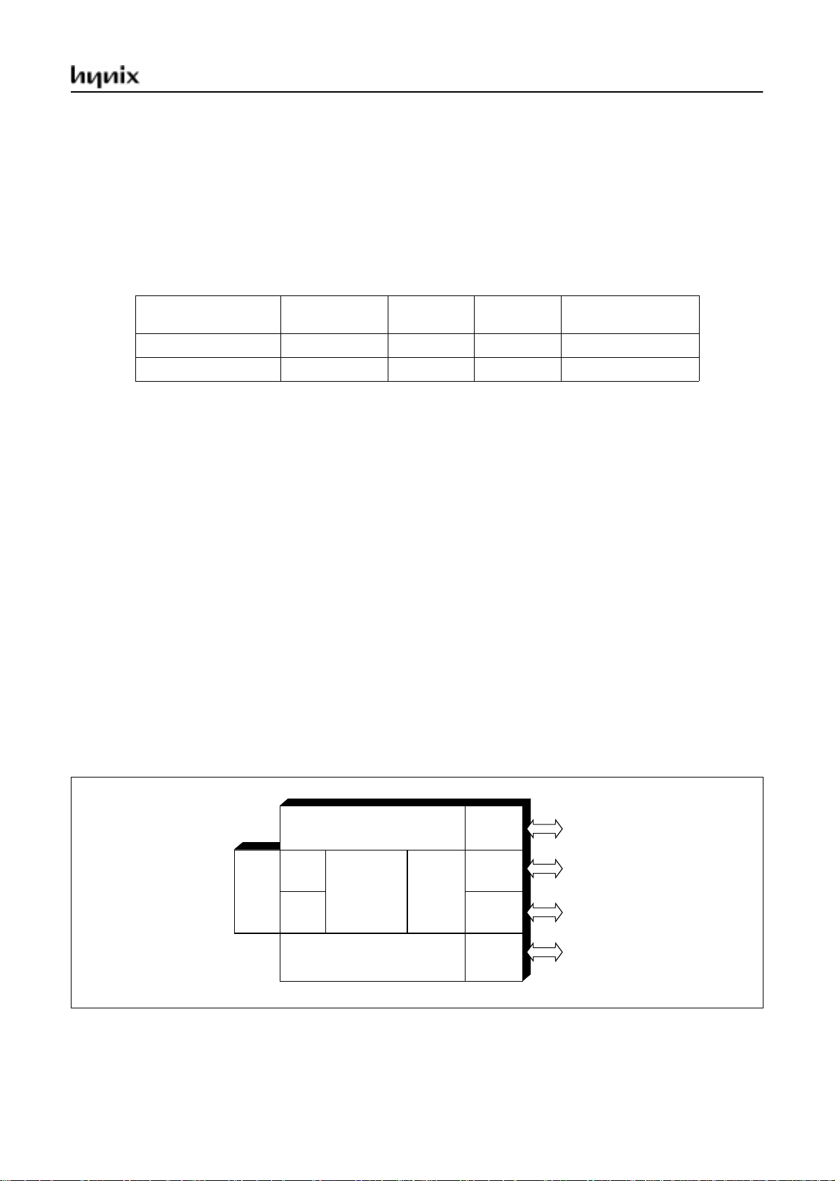
• Fully compatible to standard MCS-51 microcontroller
• Versions for 40/50 MHz operating frequency
• Low voltage version for 24MHz operating frequency
• 256 bytes of on-chip data RAM
• 64K external program memory space
• 64K external data memory space
• Four 8-bit ports
• Three 16-bit Timers/Counters (Timer 2 with up/down counter feature)
•USART
• Six interrupt sources, two priority levels
• Power saving Idle and power down mode
Operating
Frequency (MHz)
• 2.7Volt low voltage version available
• P-DIP-40, P-LCC-44, P-MQFP-44 package
RAM
256 x 8
T0
T2
T1
The GMS90C320 described in this document is compatible with the standard 80C32 can be used for all present standard
80C32 applications.
CPU
ROM-less
8-BIT
USART
PORT0
PORT1
PORT2
PORT3
I/O
I/O
I/O
I/O
OCT. 2000 Ver 1.2 1

GMS90C320
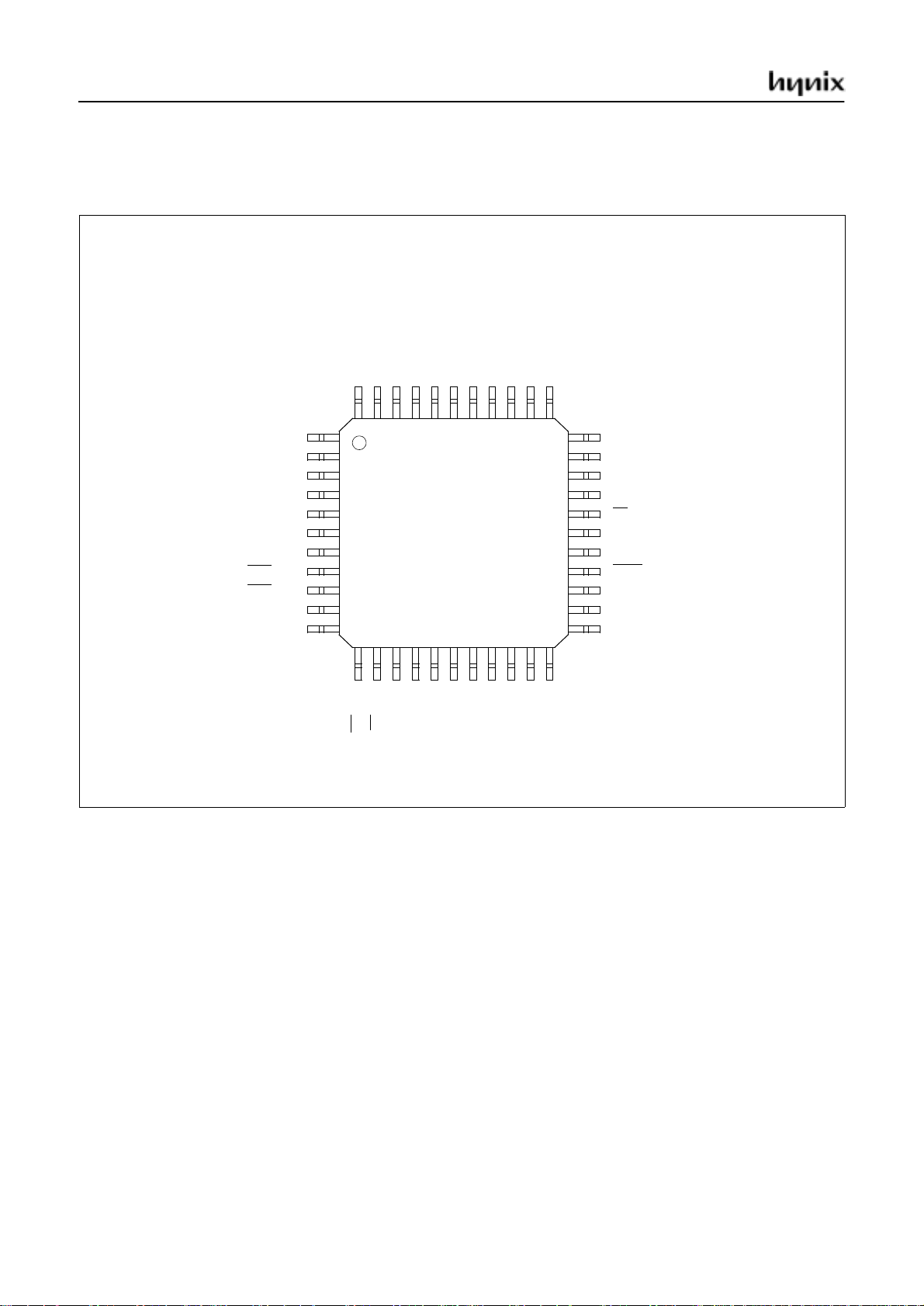
44-PLCC Pin Configuration
(top view)
RESET
RxD/P3.0
TxD/P3.1
INT0
/P3.2
INT1
/P3.3
T0/P3.4
T1/P3.5
P1.5
P1.6
P1.7
N.C.
(P-LCC-44)
P1.4
P1.2
P1.1/T2EX
P1.0/T2
N.C.
2
1
VCCP0.0/AD0
4443424140
P1.3
6
543
7
8
9
10
11
12
13
14
15
16
17
1819202122232425262728
P0.1/AD1
P0.2/AD2
P0.3/AD3
P0.4/AD4
39
P0.5/AD5
38
P0.6/AD6
37
P0.7/AD7
36
EA
35
N.C.
34
ALE
33
PSEN
32
P2.7/A15
31
P2.6/A14
30
P2.5/A13
29
/P3.6RD/P3.7
WR
SS
N.C.
V
XTAL2
XTAL1
P2.0/A8
P2.1/A9
P2.2/A10
P2.3/A11
P2.4/A12
2 OCT. 2000 Ver 1.2

40-PDIP Pin Configuration
(top view)
GMS90C320
(P-DIP-40)
T2/P1.0
T2EX/P1.1
P1.2
P1.3
P1.4
P1.5
P1.6
P1.7
RESET
RxD/P3.0
TxD/P3.1
INT0
/P3.2
INT1
/P3.3
T0/P3.4
T1/P3.5
/P3.6
WR
RD
/P3.7
XTAL2
XTAL1
V
1
2
3
4
5
6
7
8
9
10
11
12
13
14
15
16
17
18
19
20
SS
V
40
CC
P0.0/AD0
39
P0.1/AD1
38
P0.2/AD2
37
P0.3/AD3
36
35
P0.4/AD4
34
P0.5/AD5
33
P0.6/AD6
32
P0.7/AD7
31
EA
30
ALE
29
PSEN
P2.7/A15
28
P2.6/A14
27
P2.5/A13
26
P2.4/A12
25
P2.3/A11
24
P2.2/A10
23
P2.1/A9
22
P2.0/A8
21
OCT. 2000 Ver 1.2 3

GMS90C320
44-PLCC Pin Configuration
(top view)
(P-MQFP-44)
P1.4
P1.2
P1.1/T2EX
P1.0/T2
N.C.
VCCP0.0/AD0
P0.1/AD1
P0.2/AD2
P1.3
P0.3/AD3
P1.5
P1.6
P1.7
RESET
RxD/P3.0
N.C.
TxD/P3.1
INT0
/P3.2
INT1
/P3.3
T0/P3.4
T1/P3.5
4443424140
1
2
3
4
5
6
7
8
9
10
11
1213141516171819202122
/P3.6RD/P3.7
XTAL2
WR
XTAL1
3837363534
39
SS
N.C.
V
P2.0/A8
P2.1/A9
P2.2/A10
33
32
31
30
29
28
27
26
25
24
23
P2.3/A11
P2.4/A12
P0.4/AD4
P0.5/AD5
P0.6/AD6
P0.7/AD7
EA
N.C.
ALE
PSEN
P2.7/A15
P2.6/A14
P2.5/A13
4 OCT. 2000 Ver 1.2

GMS90C320
V
V
CC
SS
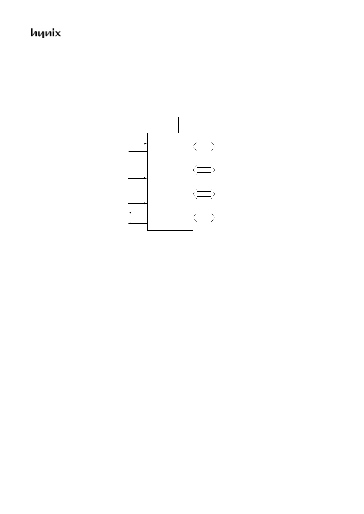
Logic Symbol
XTAL1
XTAL2
RESET
EA
ALE
PSEN
Port 0
8-bit Digital I/O
Port 1
8-bit Digital I/O
Port 2
8-bit Digital I/O
Port 3
8-bit Digital I/O
OCT. 2000 Ver 1.2 5

GMS90C320
Pin Definitions and functions
Pin Number
Symbol
P-LCC-44 P-DIP-40
P1.0-P1.7 2-9 1-8 40-44,
2
3
P3.0-P3.7 11,13-1910-17 5,7-
11 10 5 P3.0/RxD receiver data input (asynchronous) or data input
13 11 7 P3.1 / TxD transmitter data output (asynchronous) or clock
14 12 8 P3.2 / INT0 interrupt 0 input /timer0gatecontrol
15 13 9 P3.3 / INT1 interrupt 1 input /timer1gatecontrol
16 14 10 P3.4 / T0 counter 0 input
17 15 11 P3.5 / T1 counter 1 input
18 16 12 P3.6 / WR the write control signal latches the data byte from
19 17 13 P3.7 / RD the read control signal enables the external data
XTAL2 20 18 14 O XTAL2
XTAL1 21 19 15 I XTAL1
P-MQFP-
44
1-3
1
2
40
41
13
Input/
Output
I/O Port1
is an 8-bit bidirectional I/O port with internal pull-ups. Port 1 pins
that have 1s written to them are pulled high by the internal pull-up
resistors and can be used as inputs. As inputs, port 1 pins that are
externally pulled low will source current because of the pulls-ups
(IIL, in the DC characteristics). Pins P1.0 and P1.1 also. Port 1
also receives the low-order address byte during program memory
verification. Port1 also serves alternate functions of Timer 2.
P1.0/T2: Timer/counter 2 external count input
P1.1/T2EX: Timer/counter 2 trigger input
I/O Port 3
is an 8-bit bidirectional I/O port with internal pull-ups. Port 3 pins
that have 1s written to them are pulled high by the internal pull-up
resistors, and in that state they can be used as inputs. As inputs,
port 3 pins being externally pulled low will source current (IIL,in
the DC characteristics) because of internal pulls-up resistors. Port
3 also serves the special features of the 80C51 family, as listed
below.
Output of the inverting oscillator amplifier
Input to the inverting oscillator amplifier and input to the internal
clock generator circuits.
To drive the device from an external clock source, XTAL1 should
be driven, while XTAL2 is left unconnected. There are no requirements on the duty cycle of the external clock signal, since the
input to the internal clocking circuitry is divided down by a divideby-two flip-flop. Minimum and maximum high and low times as
well as rise fall times specified in the AC characteristics must be
observed.
Function
output (synchronous) of the serial interface 0
output (synchronous) of the serial interface 0
port 0 into the external data memory
memory to port 0
6 OCT. 2000 Ver 1.2

GMS90C320
Symbol
Pin Number
P-LCC-44 P-DIP-40
P-MQFP-
44
Input/
Output
P2.0-P2.7 24-31 21-28 18-25 I/O Port 2
Port 2 is an 8-bit bidirectional I/O port with internal pull-ups. Port 2
pins that have 1s written to them are pulled high by the internal
pull-up resistors and can be used as inputs. As inputs, port 2 pins
that are externally pulled low will source current because of the
pulls-ups (IIL, in the DC characteristics). Port 2 emits the highorder address byte during fetches from external program memory
and during accesses to external data memory that use 16-bit
addresses (MOVX @DPTR). In this application it uses strong
internal pull-ups when emitting 1s. During accesses to external
data memory that use 8-bit addresses (MOVX @Ri), port 2 emits
the contents of the P2 special function register.
PSEN 32 29 26 O The Program Store Enable
The read strobe to external program memory when the device is
executing code from the external program memory. PSEN is activated twice each machine cycle, except that two PSEN activation
are skipped during each access to external data memory. PSEN
is not activated during fetches from internal program memory.
RESET 10 9 4 I RESET
A high level on this pin for two machine cycles while the oscillator
is running resets the device. An internal diffused resistor to V
permits power-on reset using only an external capacitor to VCC.
ALE 33 30 27 O The Address Latch Enable
Output pulse for latching the low byte of the address during an
access to external memory. In normal operation, ALE is emitted
at a constant rate of 1/6 the oscillator frequency, and can be used
for external timing or clocking. Note that one ALE pulse is skipped
during each access to external data memory.
EA 35 31 29 I External Access Enable
EA must be external held low to enable the device to fetch code
from external program memory locations 0000Hto FFFFH.IfEAis
held high, the device executes from internal program memory
unless the program counter contains an address greater than its
internal memory size.
P0.0-P0.7 43-36 39-32 37-30 I/O Port 0
Port 0 is an 8-bit open-drain bidirectional I/O port. Port 0 pins that
have 1s written to them float and can be used as high-impedance
inputs. Port 0 is also the multiplexed low-order address and data
bus during accesses to external program and data memory. In
this application it uses strong internal pull-ups when emitting 1s.
Port 0 also outputs the code bytes during program verification in
the GMS97C5x. External pull-up resistors are required during
program verification.
V
SS
V
CC
N.C. 1,12,
22 20 16 - Circuit ground potential
44 40 38 - Supply terminal for all operating modes
23,34
-
6,17,
28,39
- No connection
Function
SS
OCT. 2000 Ver 1.2 7

GMS90C320
Function Description
The GMS90 series is fully compatible to the standard 8051 microcontroller family.
It is compatible with the standard 80C32. While maintaining all architectural and operational characteristics of the standard
80C32, the GMS90C320 incorporates some enhancements in the Timer 2 unit.
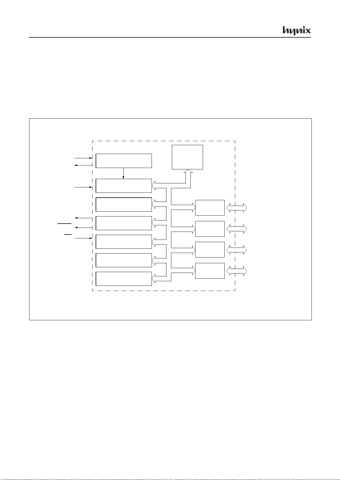
Figure 1 shows a block diagram of the GMS90C320
XTAL1
XTAL2
RESET
ALE
PSEN
EA
OSC & Timing
CPU
Timer 0
Timer 1
Timer 2
Interrupt Unit
Serial Channel
RAM
256 x 8
Port 0
Port 1
Port 2
Port 3
Port 0
8-bit Digital I/O
Port 1
8-bit Digital I/O
Port 2
8-bit Digital I/O
Port 3
8-bit Digital I/O
Figure 1 Block Diagram of the GMS90C320
8 OCT. 2000 Ver 1.2

GMS90C320
CPU
The GMS90C320is efficientbothasa controller and as an arithmetic processor.IthasextensivefacilitiesforbinaryandBCD
arithmetic and excels in its bit-handling capabilities. Efficient use of program memory results from an instruction set consisting of 44% one-byte, 41% two-byte, and 15% three-byte instructions. With a 12 MHz crystal, 58% o f the instructions are
executed in 1.0µs.
Special Function R egister PSW
MSB LSB
BitNo.76543210
Addr. D0
CY AC F0 RS1 RS2 OV F1 P PSW
H
Bit Function
CY Carry Flag
AC Auxiliary Carry Flag (for BCD operation)
F0 General Purpose Flag
RS1
0
0
1
1
RS0
0
1
0
1
Register Bank select control bits
Bank 0 selected, data address 00H-07
Bank 1 selected, data address 08H-0F
Bank 2 selected, data address 10H-17
Bank 3 selected, data address 18H-1F
OV Overflow Flag
F1 General Purpose Flag
P Parity Flag
Set/cleared by hardware each instruction cycle to indicate an odd/
even number of “one” bits in the accumulator, i.e. even parity.
Reset value of PSW is 00
H.
H
H
H
H
OCT. 2000 Ver 1.2 9

GMS90C320
Special Function Registers
All registers, except the program counter and the four general purpose register banks, reside in the special function register
area.
The 27 special function registers (SFR) include pointers and registers that provide an interface between theCPUand the other
on-chip peripherals. There are also 128 directly addressable bits within the SFR area.
All SFRs are listed in Table 1, Table 2,andTable 3.
In Table 1 they are organized in numeric order of their addresses. In Table 2 they are organized in groups which refer to the
functional blocks of the GMS90C320. Table 3 illustrates the contents of the SFRs.
Table 1
Special Function Registers in Numeric Order of their Addresses
Address Register
80
H
81
H
82
H
83
H
84
H
85
H
86
H
87
H
88
H
89
H
8A
H
8B
H
8C
H
8D
H
8E
H
8F
H
90
H
91
H
92
H
93
H
94
H
95
H
96
H
97
H
98
H
99
H
9A
H
9B
H
9C
H
9D
H
9E
H
9F
H
1)
: Bit-addressable Special Function Register
2)
: X means that the value is indeterminate and the location is reserved
1)
P0
SP
DPL
DPH
reserved
reserved
reserved
PCON
TCON
TMOD
TL0
TL1
TH0
TH1
reserved
reserved
1)
P1
reserved
reserved
reserved
reserved
reserved
reserved
reserved
SCON
SBUF
reserved
reserved
reserved
reserved
reserved
reserved
1)
1)
Contents after
Reset
FF
H
07
H
00
H
00
H
2)
XX
H
2)
XX
H
2)
XX
H
00
00
00
00
00
00
FF
00
00
2)
B
H
H
H
H
H
H
2)
H
2)
H
H
H
2)
H
2)
H
2)
H
2)
H
2)
H
2)
H
H
2)
H
2)
H
2)
H
2)
H
2)
H
2)
H
2)
H
0XXX0000
XX
XX
XX
XX
XX
XX
XX
XX
XX
XX
XX
XX
XX
XX
XX
Address Register
A0
A1
A2
A3
A4
A5
A6
A7
A8
A9
AA
AB
AC
AD
AE
AF
B0
B1
B2
B3
B4
B5
B6
B7
B8
B9
BA
BB
BC
BD
BE
BF
H
H
H
H
H
H
H
H
H
H
H
H
H
H
H
H
H
H
H
H
H
H
H
H
H
H
H
H
H
H
H
H
1)
P2
reserved
reserved
reserved
reserved
reserved
reserved
reserved
1)
IE
reserved
reserved
reserved
reserved
reserved
reserved
reserved
1)
P3
reserved
reserved
reserved
reserved
reserved
reserved
reserved
1)
IP
reserved
reserved
reserved
reserved
reserved
reserved
reserved
Contents after
Reset
FF
H
2)
XX
H
2)
XX
H
2)
XX
H
2)
XX
H
2)
XX
H
2)
XX
H
2)
XX
H
FF
2)
B
2)
H
2)
H
2)
H
2)
H
2)
H
2)
H
2)
H
H
2)
H
2)
H
2)
H
2)
H
2)
H
2)
H
2)
H
2)
B
2)
H
2)
H
2)
H
2)
H
2)
H
2)
H
2)
H
0X000000
XX
XX
XX
XX
XX
XX
XX
XX
XX
XX
XX
XX
XX
XX
XX000000
XX
XX
XX
XX
XX
XX
XX
10 OCT. 2000 Ver 1.2
 Loading...