HYNIX GMS87C1408SK, GMS87C1408D, GMS87C1408, GMS87C1404SK, GMS87C1404D Datasheet
...
June. 2001 Ver 1.2
8-BIT SINGLE-CHIP MICROCONTROLLERS
GMS81C1404
GMS81C1408
User’s Manual

Table of Contents
OVERVIEW . . . . . . . . . . . . . . . . . . . . . . . 1
Description . . . . . . . . . . . . . . . . . . . . . . 1
Features . . . . . . . . . . . . . . . . . . . . . . . . 1
Development Tools . . . . . . . . . . . . . . . . 2
Ordering Information . . . . . . . . . . . . . . . 2
BLOCK DIAGRAM . . . . . . . . . . . . . . . . . 3
PIN ASSIGNMENT . . . . . . . . . . . . . . . . . 4
PACKAGE DIAGRAM . . . . . . . . . . . . . . . 5
PIN FUNCTION . . . . . . . . . . . . . . . . . . . . 6
PORT STRUCTURES . . . . . . . . . . . . . . . 8
ELECTRICAL CHARACTERISTICS
(GMS81C1404/GMS81C1408) . . . . . . . 12
Absolute Maximum Ratings . . . . . . . . 12
Recommended Operating Conditions 12
A/D Converter Characteristics . . . . . . 12
DC Electrical Characteristics . . . . . . . 13
AC Characteristics . . . . . . . . . . . . . . . 14
Typical Characteristics . . . . . . . . . . . . 15
ELECTRICAL CHARACTERISTICS
(GMS87C1404/GMS87C1408) . . . . . . . 17
Absolute Maximum Ratings . . . . . . . . 17
Recommended Operating Conditions 17
A/D Converter Characteristics . . . . . . 17
DC Electrical Characteristics . . . . . . . 18
AC Characteristics . . . . . . . . . . . . . . . 19
Typical Characteristics . . . . . . . . . . . . 20
MEMORY ORGANIZATION . . . . . . . . . 22
Registers . . . . . . . . . . . . . . . . . . . . . . 22
Program Memory . . . . . . . . . . . . . . . . 24
Data Memory . . . . . . . . . . . . . . . . . . . 27
Addressing Mode . . . . . . . . . . . . . . . . 31
I/O PORTS . . . . . . . . . . . . . . . . . . . . . . 35
RA and RAIO registers . . . . . . . . . . . . 35
RB and RBIO registers . . . . . . . . . . . . 36
RC and RCIO registers . . . . . . . . . . . . 38
RD and RDIO registers . . . . . . . . . . . . 39
CLOCK GENERATOR . . . . . . . . . . . . . . 40
Oscillation Circuit . . . . . . . . . . . . . . . . .40
BASIC INTERVAL TIMER . . . . . . . . . . . 41
TIMER / COUNTER . . . . . . . . . . . . . . . .42
8-bit Timer/Counter Mode . . . . . . . . . .43
16-bit Timer/Counter Mode . . . . . . . . .45
8-bit Compare Output (16-bit) . . . . . . .45
8-bit Capture Mode . . . . . . . . . . . . . . . 45
16-bit Capture Mode . . . . . . . . . . . . . .48
PWM Mode . . . . . . . . . . . . . . . . . . . . . 48
SERIAL PERIPHERAL INTERFACE . . .51
BUZZER OUTPUT FUNCTION . . . . . . .53
ANALOG TO DIGITAL CONVERTER . .54
INTERRUPTS . . . . . . . . . . . . . . . . . . . .57
Interrupt Sequence . . . . . . . . . . . . . . .59
BRK Interrupt . . . . . . . . . . . . . . . . . . . .60
Multi Interrupt . . . . . . . . . . . . . . . . . . . .60
External Interrupt . . . . . . . . . . . . . . . . . 62
WATCHDOG TIMER . . . . . . . . . . . . . . .64
POWER SAVING MODE . . . . . . . . . . . .65
Stop Mode . . . . . . . . . . . . . . . . . . . . . .65
STOP Mode using Internal RCWDT . . 67
Wake-up Timer Mode . . . . . . . . . . . . . 68
Minimizing Current Consumption . . . .69
RESET . . . . . . . . . . . . . . . . . . . . . . . . . . 71
POWER FAIL PROCESSOR . . . . . . . . . 72
OTP PROGRAMMING (GMS87C1404/
GMS87C1408 ONLY) . . . . . . . . . . . . . . .74
DEVICE CONFIGURATION AREA . . . 74
A. INSTRUCTION MAP . . . . . . . . . . . . . i
B. INSTRUCTION SET . . . . . . . . . . . . . ii

GMS81C1404/GMS81C1408
GMS81C1404 / GMS81C1408
CMOS SINGLE-CHIP 8-BIT MICROCONTROLLER
1. OVERVIEW
1.1 Description
The GMS81C1404 and GMS81C14 08 are an ad vanced C MOS 8 -bi t microcontroller with 4K/8K bytes of ROM. The Hynix
semiconductor’s GMS81C 1404 and GMS81C1408 are a power ful microcont roller which prov ides a highly flexib le and cost
effective solution to many small applications such as controller for battery charger. The GMS81C1404 and GMS81C1408
provide the followi ng st an dard feat ur es: 4 K/8K bytes of ROM, 192 bytes of RAM, 8-bit t i mer /co un ter , 8 -bi t A/D converter,
10-bit high speed PWM output, programmable buzzer driving port, 8-bit serial communication port, on-chip oscillator and
clock circuitry. In addition, the GMS81C1404 and GMS81C1408 supports power saving modes to reduce power consumption.
Device name ROM Size EPROM Size RAM Size
GMS81C1404 4K bytes - 192bytes 2.2 ~ 5.5V 28 SKDIP or SOP
GMS81C1408 8K bytes - 192bytes 2.2 ~ 5.5V 28 SKDIP or SOP
GMS87C1404 - 4K bytes 192bytes 2.5 ~ 5.5V 28 SKDIP or SOP
GMS87C1408 - 8K bytes 192bytes 2.5 ~ 5.5V 28 SKDIP or SOP
1.2 Features
• 4K/8K Bytes On-chip Program Memory
• 192 Bytes of On-chip Data RAM
(Included stack memory)
• Instruction Cycle Time:
- 250nS at 8MHz
• 23 Programmable I/O pins
(LED direct driving can be source and sink)
• 2.2V to 5.5V Wide Operating Range
• One 8-bit A/D Converter
• One 8-bit Basic Interval Timer
• Four 8-bit Timer / Counters
• Two 10-bit High Speed PWM Outputs
• Watchdog timer (can be operate with internal
RC-oscillation)
Operatind
Voltage
• One 8-bit Serial Peripheral Interface
• Twelve Interrupt sources
- External input: 4
- A/D Conversion: 1
- Serial Peripheral Interface: 1
- Timer: 6
• One Programmable Buzzer Driving port
- 500Hz ~ 130kHz
• Oscillator Type
- Crystal
- Ceramic Resonator
• Noise Immunity Circuit
- Power Fail Processor
• Power Down Mode
- STOP mode
- Wake-up Timer mode
Package
June. 2001 Ver 1.2 1

GMS81C1404/GMS81C1408
1.3 Development Tools
The GMS81C1404 and GMS81C1408 are supported by a
full-featured macro assembler, an in-circuit emulator
CHOICE-Dr
TM
.
1.4 Ordering Information
ROM Size Package Type Ordering Device Code Operating Temperature
28SKDIP GMS81C1404 SK
4K bytes
8K bytes
4K bytes (OTP)
8K bytes (OTP)
28SOP GMS81C1404 D
28SKDIP GMS81C1404E SK
28SOP GMS81C1404E D
28SKDIP GMS81C1408 SK
28SOP GMS81C1408 D
28SKDIP GMS81C1408E SK
28SOP GMS81C1408E D
28SKDIP GMS87C1404 SK
28SOP GMS87C1404 D
28SKDIP GMS87C1408 SK
28SOP GMS87C1408 D
In Circuit Emulators
Assembler
OTP Writer
OTP Devices
CHOICE-Dr.
HME Macro Assembler
Single Writer : Dr. Writer
4-Gang Writer : Dr.Gang
GMS87C1404 SK (Skinny DIP)
GMS87C1404 D (SOP)
GMS87C1408 SK (Skinny DIP)
GMS87C1408 D (SOP)
-20 ~ +85
-40 ~ +85
-20 ~ +85
-40 ~ +85
-20 ~ +85
C
°
C
°
C
°
C
°
C
°
2
June. 2001 Ver 1.2
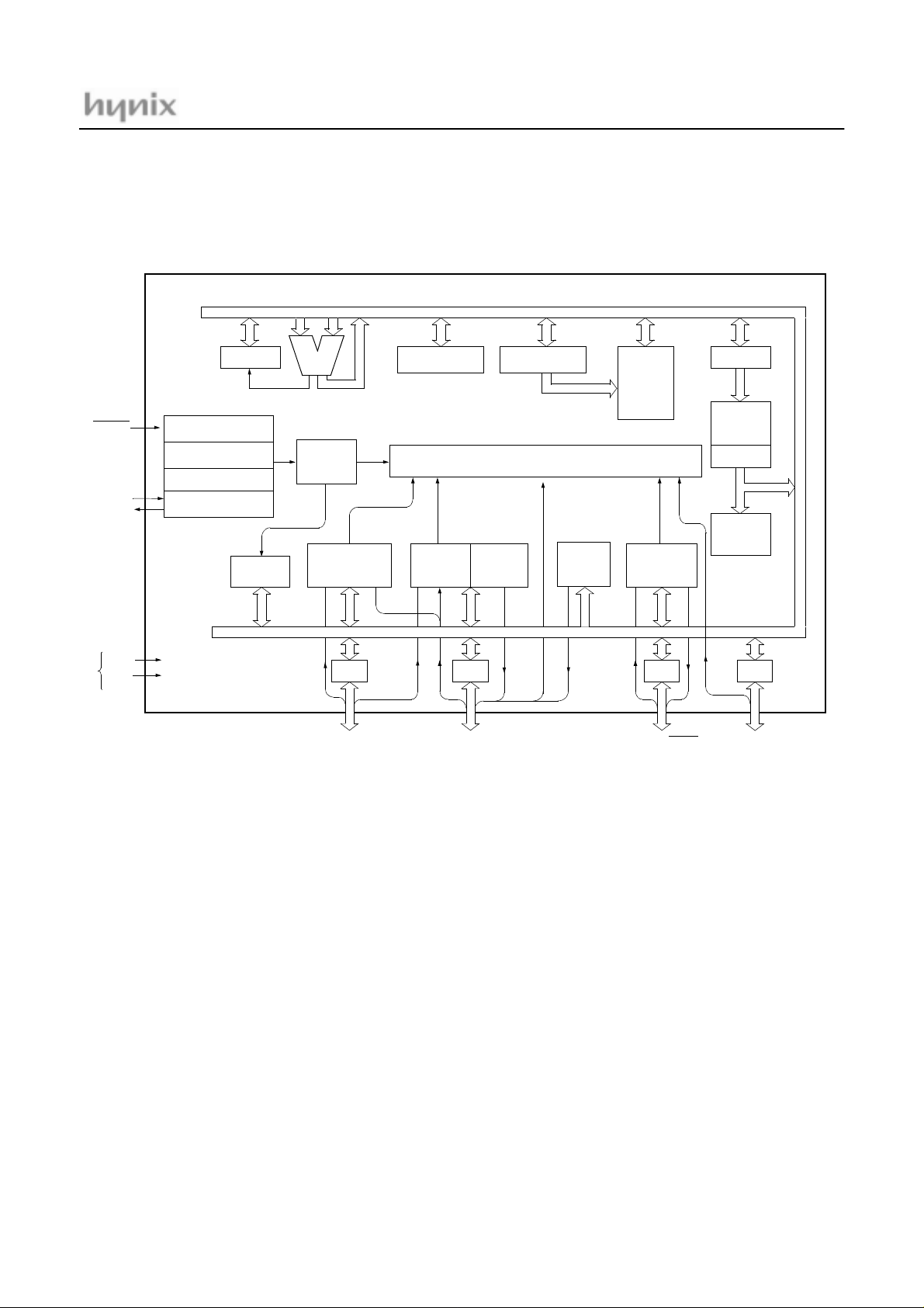
2. BLOCK DIAGRAM
GMS81C1404/GMS81C1408
RESET
Xin
Xout
V
DD
V
SS
Power
Supply
PSW
System controller
System
Clock Controller
Timing generator
Clock Generator
Watch-dog
Timer
ALU
8-bit Basic
Interval
Timer
8-bit
A/D
Converter
RA RB RC
RA0 / EC0
RA1 / AN1
RA2 / AN2
RA3 / AN3
RA4 / AN4
RA5 / AN5
RA6 / AN6
RA7 / AN7
Accumulator Stack Pointer
Interrupt Controller
8-bit
Timer/
Counter
High
Speed
PWM
RB0 / AN0 / Avref
RB1 / BUZ
RB2 / INT0
RB3 / INT1
RB4 / CMP0 / PWM0
RB5 / CMP1 / PWM1
RB6 / EC1
RB7 / TMR2OV
Buzzer
Driver
Data
Memory
SPI
RC3 / SRDY
RC4 / SCK
RC5 / SIN
RC6 / SOUT
PC
Program
Memory
Data Table
Instruction
Decoder
RD
RD0 / INT2
RD1 / INT3
RD2
June. 2001 Ver 1.2 3
GMS81C1404/GMS81C1408
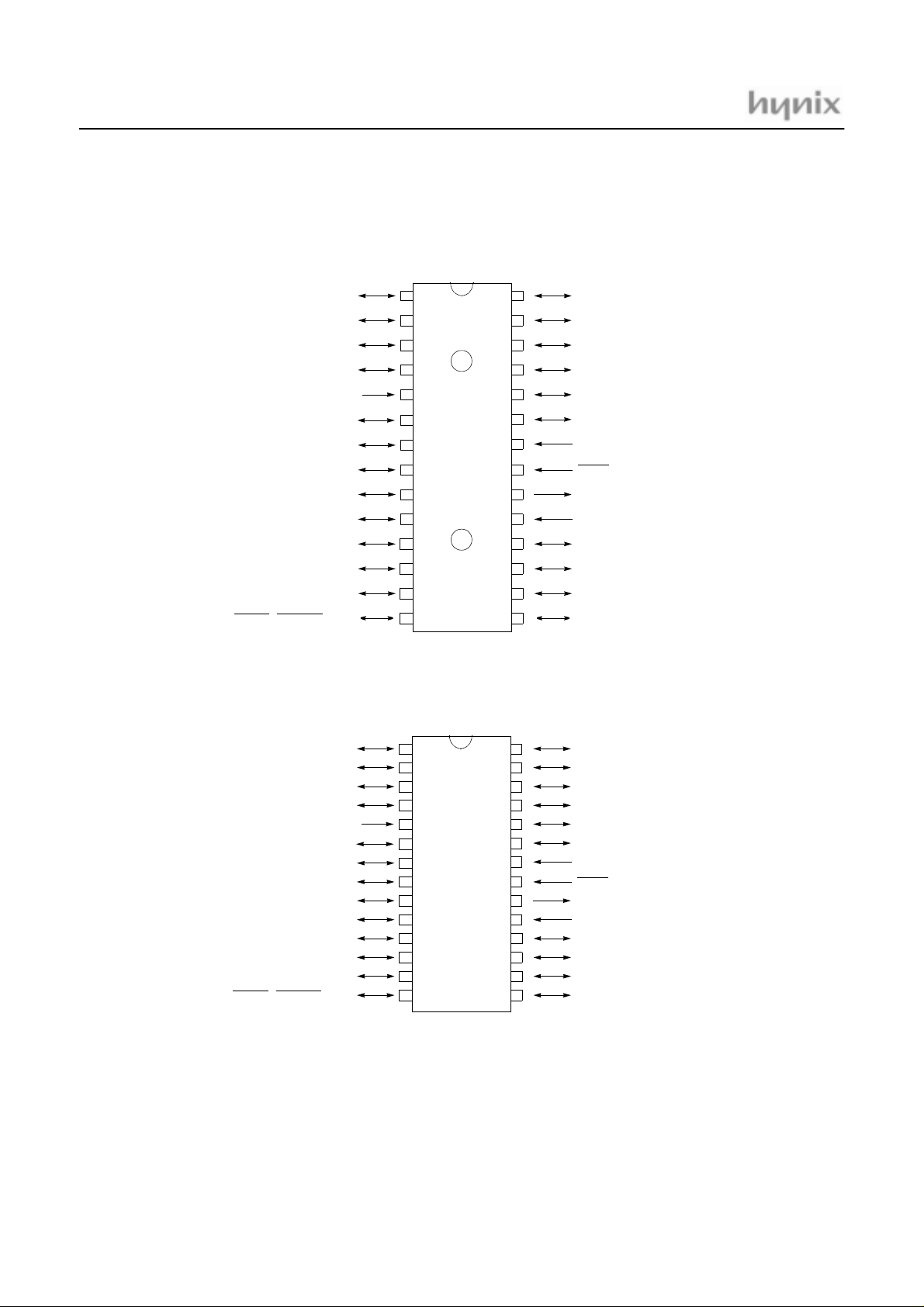
3. PIN ASSIGNMENT
28 SKINNY DIP
AN4 / RA4
AN5 / RA5
AN6 / RA6
AN7 / RA7
V
DD
AN0 / AVref / RB0
BUZ / RB1
INT0 / RB2
INT1 / RB3
PWM0 / COMP0 / RB4
PWM1 / COMP1 / RB5 RD2
EC1 / RB6
TMR2OV / RB7
SRDYIN / SRDYOUT / RC3
1
2
3
4
5
6
7
8
9
10
11
12
13
14
28
27
26
25
24
23
22
21
20
19
18
17
16
15
28 SOP
RA3 / AN3
RA2 / AN2
RA1 / AN1
RA0 / EC0
RD1 / INT3
RD0 / INT2
V
SS
RESET
Xout
Xin
RC6 / SOUT
RC5 / SIN
RC4 / SCK
AN4 / RA4
AN5 / RA5
AN6 / RA6
AN7 / RA7
V
DD
AN0 / AVref / RB0
BUZ / RB1
INT0 / RB2
INT1 / RB3
PWM0 / COMP0 / RB4
PWM1 / COMP1 / RB5 RD2
EC1 / RB6
TMR2OV / RB7
SRDYIN / SRDYOUT / RC3
1
2
3
4
5
6
7
8
9
10
11
12
13
14
28
27
26
25
24
23
22
21
20
19
18
17
16
15
RA3 / AN3
RA2 / AN2
RA1 / AN1
RA0 / EC0
RD1 / INT3
RD0 / INT2
V
SS
RESET
Xout
Xin
RC6 / SOUT
RC5 / SIN
RC4 / SCK
4
June. 2001 Ver 1.2
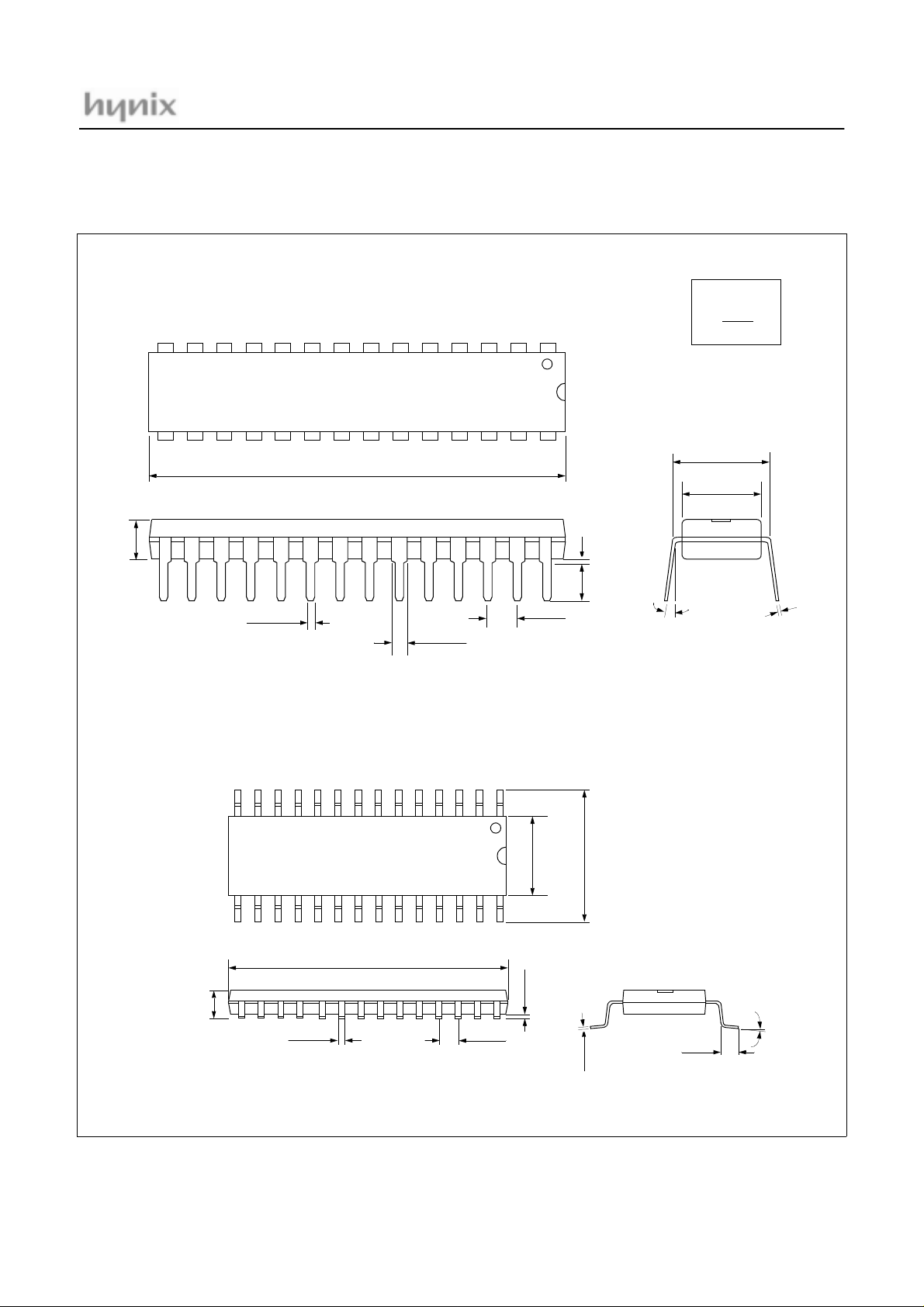
4. PACKAGE DIAGRAM
GMS81C1404/GMS81C1408
28 SKINNY DIP
MAX 0.180
0.021
0.015
1.375
1.355
0.055
0.045
TYP 0.100
0.140
MIN 0.020
0.120
0 ~ 15°
unit: inch
MAX
MIN
TYP 0.300
0.300
0.275
4
1
0
.
0
8
0
0
.
0
28 SOP
0.293
0.006
0.414
0.012
0.398
0.008
0.042
0 ~ 8°
0.022
0.299
0.708
0.608
0.012
0.106
0.096
0.019
0.013
TYP 0.050
June. 2001 Ver 1.2 5

GMS81C1404/GMS81C1408
5. PIN FUNCTION
VDD: Supply voltage.
V
: Circuit ground.
SS
RESET
X
: Reset the MCU.
: Input to the inverting oscillator amplifier and input to
IN
the internal main clock operating circuit.
X
: Output from the inverting oscillator amplifier.
OUT
RA0~RA7: RA is an 8-bit, CMOS, bidirectional I/O port.
RA pins can be used as outputs or inputs according to “1”
or “0” written the their Port Direction Register(RAIO).
Port pin Alternate function
RA0
RA1
RA2
RA3
RA4
RA5
RA6
RA7
EC0 ( Event Counter Input Source )
AN1 ( Analog Input Port 1 )
AN2 ( Analog Input Port 2 )
AN3 ( Analog Input Port 3 )
AN4 ( Analog Input Port 4 )
AN5 ( Analog Input Port 5 )
AN6 ( Analog Input Port 6 )
AN7 ( Analog Input Port 7 )
Table 5-1 RA Port
In addition, RA serves the functions of the various special
features in Table 5-1 .
RB0~RB7: RB is a 8-bit, CMOS, bidirectional I/O port.
RB pins can be used as outputs or inputs according to “1”
or “0” written the their Port Direction Register(RBIO).
RC3~RC6: RC is a 4-bit, CMOS, bidirectional I/O port.
RC pins can be used as outputs or inputs according to “1”
or “0” written the their Port Direction Register(RCIO).
RC serves the functions of the serial interface following
special features in Table 5-3 .
Port pin Alternate function
RC3
RC4
RC5
RC6
SRDYIN
SRDYOUT
SCKI (SPI CLK Input)
SCKO (SPI CLK Output)
SIN (SPI Serial Data Input)
SOUT (SPI Serial Data Output)
(SPI Ready Input)
(SPI Ready Output)
Table 5-3 RC Port
RD0~RD2: RD is a 3-bit, CMOS, bidirectional I/O port.
RC pins can be used as outputs or inputs according to “1”
or “0” written the their Port Direction Register(RDIO).
RD serves the functions of the external interrupt following
special features in Table 5-4
Port pin Alternate function
RD0
RD1
RD2
INT2 (External Interrupt Input Port 2)
INT3 (External Interrupt Input Port 3)
Table 5-4 RD Port
RB serves the functions of the va rious following special
features
in
Table 5-2
Port pin Alternate function
RB0
RB1
RB2
RB3
RB4
RB5
RB6
RB7
AN0 ( Analog Input Port 0 )
AVref ( External Analog Reference Pin )
BUZ ( Buzzer Driving Output Port )
INT0 ( External Interrupt Input Port 0 )
INT1 ( External Interrupt Input Port 1 )
PWM0 (PWM0 Output)
COMP0 (Timer1 Compare Output)
PWM1 (PWM1 Output)
COMP1 (Timer3 Compare Output)
EC1 (Event Counter Input Source)
TMR2OV (Timer2 Overflow Output)
Table 5-2 RB Port
6
June. 2001 Ver 1.2
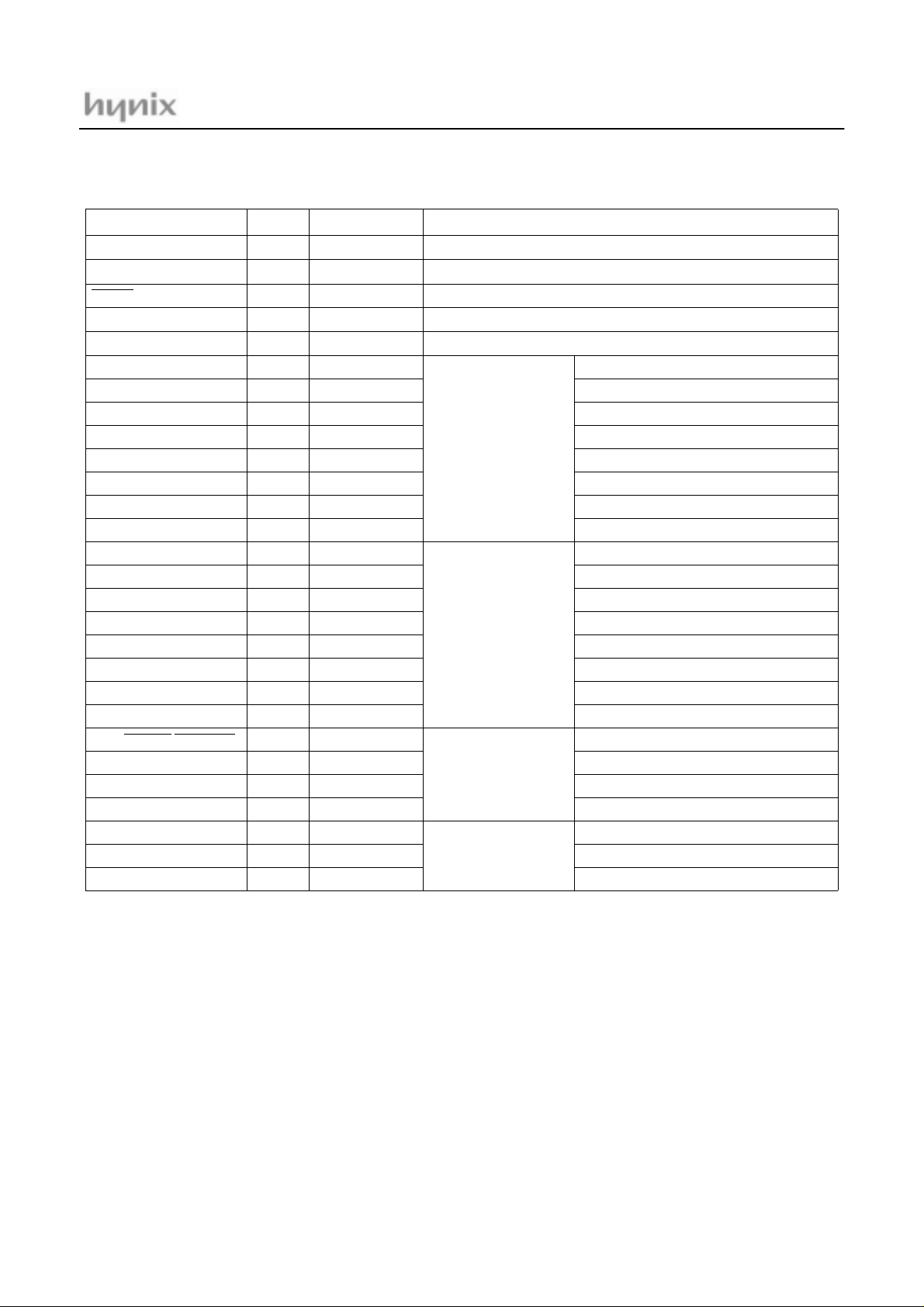
PIN NAME Pin No. In/Out Function
V
DD
V
SS
RESET
X
IN
X
OUT
22
21
19
20
RA0 (EC0) 25
RA1 (AN1) 26
RA2 (AN2) 27
RA3 (AN3) 28
RA4 (AN4) 1
RA5 (AN5) 2
RA6 (AN6) 3
RA7 (AN7) 4
RB0 (AVref/AN0) 6
RB1 (BUZ) 7
RB2 (INT0) 8
RB3 (INT1) 9
RB4 (PWM0/COMP0) 10
RB5 (PWM1/COMP1) 11
RB6 (EC1) 12
RB7 (TMR2OV) 13
RC3 (SRDYIN
/SRDYOUT)14
RC4 (SCK) 15
RC5 (SIN) 16
RC6 (SOUT) 17
RD0 (INT2) 23
RD1 (INT3) 24
RD2 18
5
-
I
I
O
I/O (Input)
I/O (Input)
I/O (Input)
I/O (Input)
I/O (Input)
I/O (Input)
I/O (Input)
I/O (Input)
I/O (Input)
I/O (Input)
I/O (Input)
I/O (Output)
I/O (Output/Output)
I/O (Output/Output)
I/O (Output/Output)
I/O (Output/Output)
I/O (Input/Output)
I/O (Input/Output)
I/O (Input)
I/O (Output)
I/O (Input)
I/O (Input)
I/O
Supply voltage
Circuit ground
Reset signal input
8-bit general I/O ports
8-bit general I/O ports
4-bit general I/O ports
3-bit general I/O ports
GMS81C1404/GMS81C1408
External Event Counter input 0
Analog Input Port 1
Analog Input Port 2
Analog Input Port 3
Analog Input Port 4
Analog Input Port 5
Analog Input Port 6
Analog Input Port 7
Analog Input Port 0 / Analog Reference
Buzzer Driving Output
External Interrupt Input 0
External Interrupt Input 1
PWM0 Output or Timer1 Compare Output
PWM1 Output or Timer3 Compare Output
External Event Counter input 1
Timer2 Overflow Output
SPI READY Input/Output
SPI CLK Input/Output
SPI DATA Input
SPI DATA Output
External Interrupt Input 2
External Interrupt Input 3
Table 5-5 Pin Description
June. 2001 Ver 1.2 7
GMS81C1404/GMS81C1408
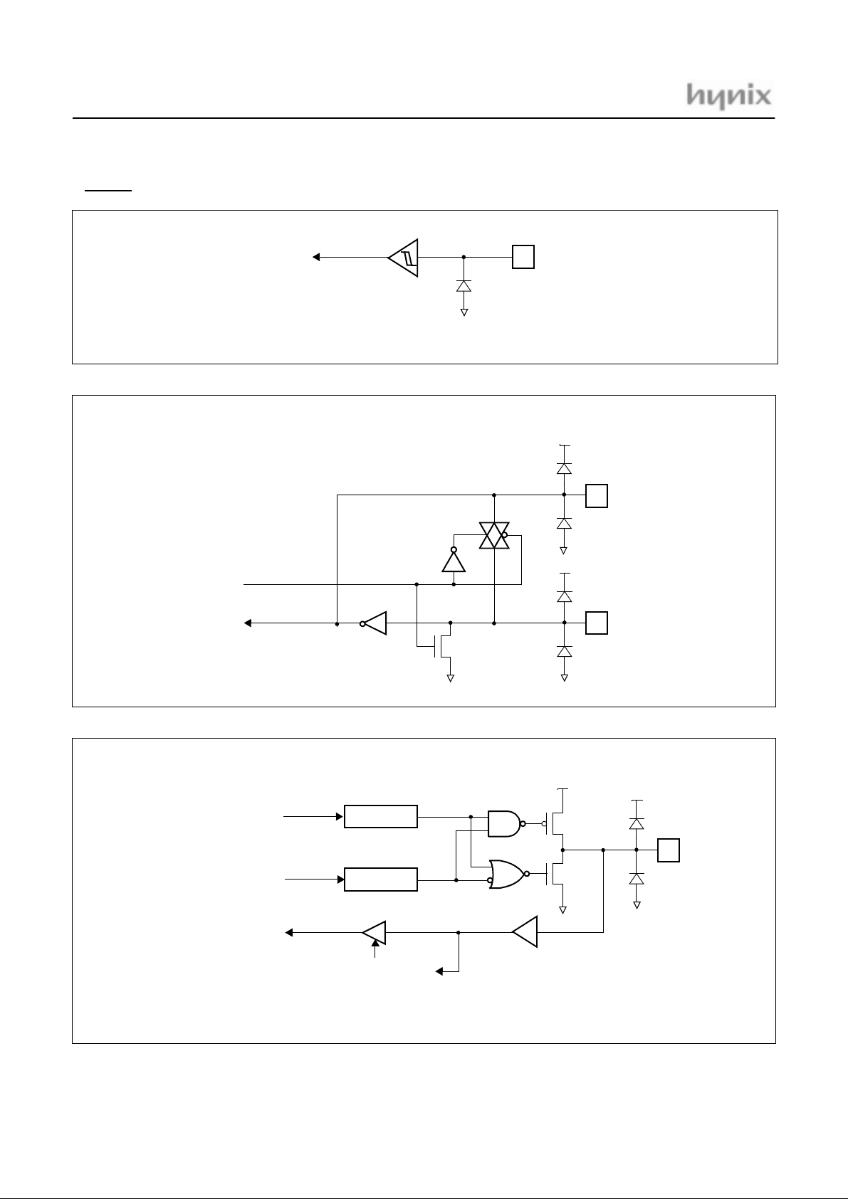
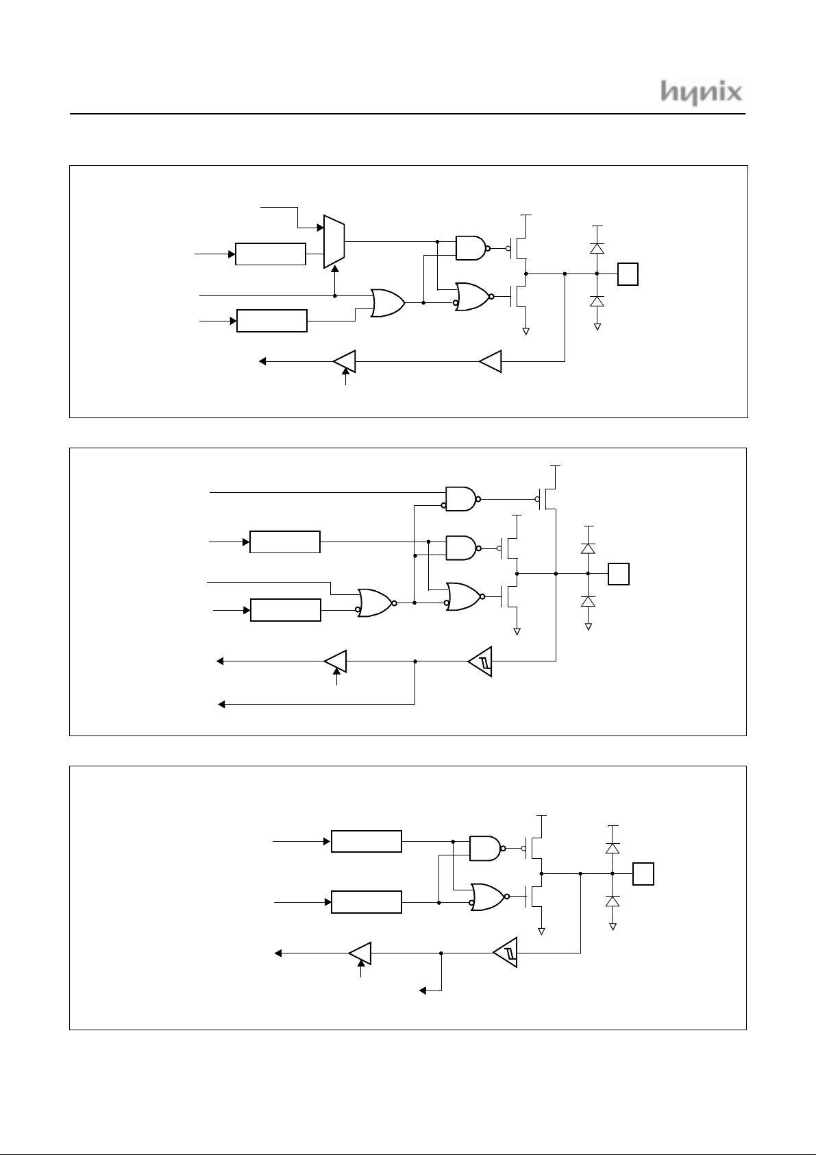
6. PORT STRUCTURES
• RESET
Internal RESET
• Xin, Xout
V
SS
V
DD
Xout
• RA0/EC0
STOP
To System CLK
Data Bus
Data Bus
Data Bus
Data Reg.
Direction Reg.
Read
EC0
V
SS
Xin
8
June. 2001 Ver 1.2
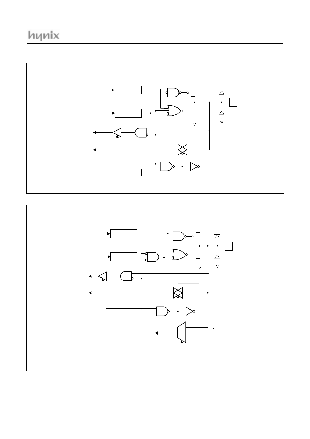
• RA1/AN1 ~ RA7/AN7
Data Bus
Data Bus
Data Bus
To A/D Converter
Analog Input Mode
(ANSEL7 ~ 1)
Analog CH. Selection
(ADCM.4 ~ 2)
Data Reg.
Direction Reg.
Read
GMS81C1404/GMS81C1408
V
DD
V
SS
• RB0 / AN0 / AVref
Data Bus
AVREFS
Data Bus
Data Bus
To A/D Converter
Analog Input Mode
(ANSEL0)
Analog CH0 Selection
(ADCM.4 ~ 2)
Read
Data Reg.
Direction Reg.
To Vref of A/D
1
0
AVREFS
V
DD
V
SS
Internal V
DD
June. 2001 Ver 1.2 9
GMS81C1404/GMS81C1408
• RB1/BUZ, RB4/PWM0/COMP0, RB5/PWM1/COMP1, RB7/TMR2OV, RC6/SOUT
PWM/COMP
BUZ,TMR2OV,SOUT
1
0
Read
Data Bus
Function
Select
Data Bus
Data Reg.
Direction Reg.
Data Bus
• RB2/INT0, RB3/INT1, RD0/INT2, RD1/INT3
Pull-up
Select
V
V
SS
DD
Weak Pull-up
• RB6/EC1
Data Bus
Function
Select
Data Bus
Data Bus
INT0, INT1
INT2, INT3
Data Bus
Data Bus
Data Reg.
Direction Reg.
Read
Data Reg.
Direction Reg.
Schmitt Trigger
V
DD
V
SS
10
Data Bus
Read
EC1
June. 2001 Ver 1.2
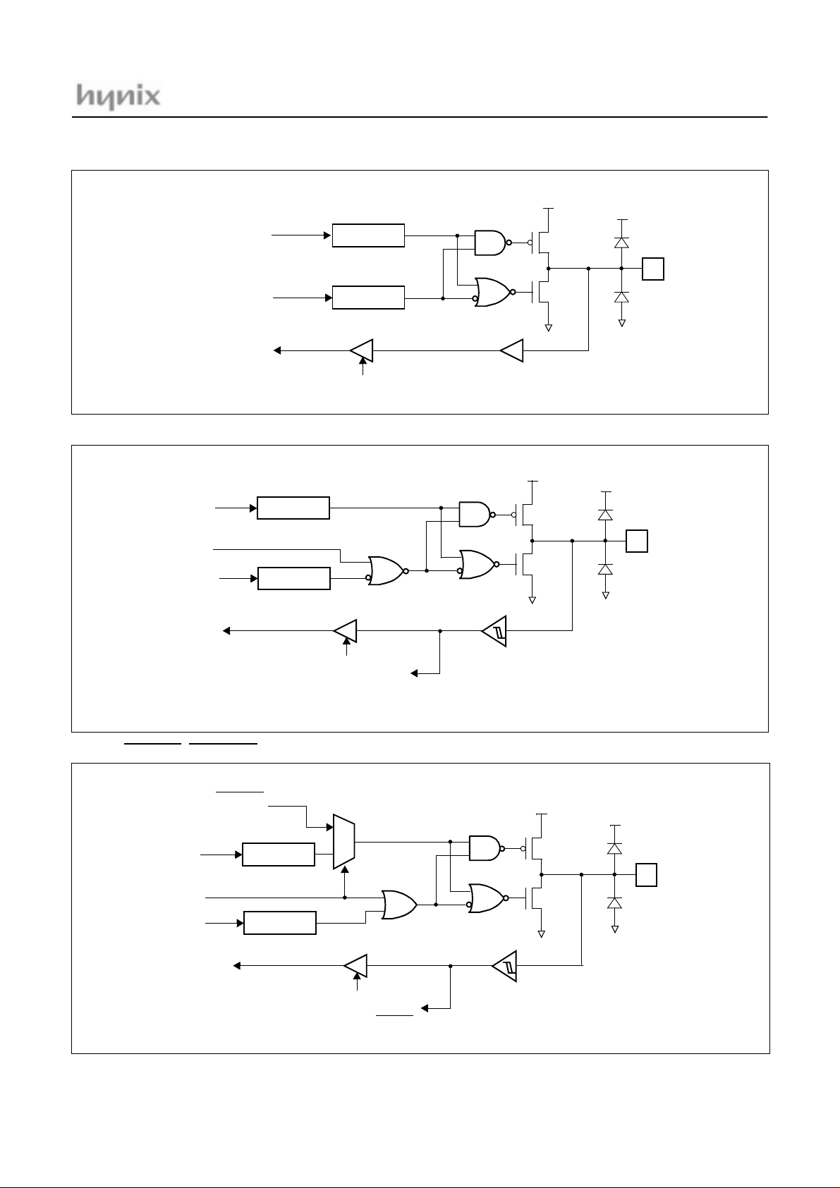
• RD2
• RC5/SIN
Data Bus
Data Bus
Data Bus
Data Reg.
Direction Reg.
Read
GMS81C1404/GMS81C1408
V
DD
V
SS
Data Bus
Function
Select
Data Bus
Data Bus
• RC3 / SRDYIN
Data Bus
Function
Select
Data Bus
Data Bus
Data Reg.
Direction Reg.
Read
SIN
/ SRDYOUT, RC4 / SCKIN / SCKOUT
SRDYOUT
SCKOUT
Data Reg.
Direction Reg.
1
0
Schmitt Trigger
V
DD
V
SS
V
DD
V
SS
Read
SCKIN
SRDYIN
Schmitt Trigger
June. 2001 Ver 1.2 11

GMS81C1404/GMS81C1408
7. ELECTRICAL CHARACTERISTICS (GMS81C1404/GMS81C1408)
7.1 Absolute Maximum Ratings
Supply voltage...........................................-0.3 to +6.0 V
Storage Temperature ................................-40 to +125 °C
Voltage on any pin with respect to Ground (V
SS
)
................................ ............................... -0.3 to VDD+0.3
Maximum current out of V
Maximum current into V
Maximum current sunk by (I
Maximum output current sourced by (I
pin........................200 mA
SS
pin ..........................150 mA
DD
per I/O Pin) ........25 mA
OL
per I/O Pin)
OH
...............................................................................15 mA
Maximum current (ΣI
) ....................................150 mA
OL
7.2 Recommended Operating Conditions
Maximum current (ΣI
Stresses above those listed under “Absolute Maxi-
Note:
mum Ratings” may cause perma nent damage to the
device. This is a stress rat ing only and functional op eration of the device at any other conditions above
those indicated in the operational sections of this
specification is not implied. Exposure to absolute
maximum rating cond itions for extended pe riods
may affect device reliability.
)....................................100 mA
OH
Parameter Symbol Condition
Supply Voltage
Operating Frequency
Operating Temperature
V
T
f
XIN
OPR
DD
7.3 A/D Converter Characteristics
(TA=25°C, VSS=0V, VDD=5.12V @
Parameter Symbol Condition
Analog Input Voltage Range
Analog Power Supply Input Voltage Range
Overall Accuracy
Non-Linearity Error
Differential Non-Linearity Error
Zero Offset Error
Full Scale Error
Gain Error
Conversion Time
AV
Input Current I
REF
f
=8MHz, VDD=3.072V @
XIN
f
=8MHz
XIN
=4.2MHz
f
XIN
VDD=4.5~5.5V
V
=2.2~5.5V
DD
V
AIN
V
REF
N
ACC
N
NLE
N
DNLE
N
ZOE
N
FSE
N
NLE
T
CONV
REF
Specifications
Unit
Min. Max.
4.5 5.5 V
2.2 5.5 V
18MHz
14.2MHz
-20 (-40 for GMS81C140XE) 85
f
=4MHz)
XIN
C
°
Specifications
Unit
Min. Typ. Max.
AVREFS=0
AVREFS=1
VDD=5V
V
=3V
DD
f
=8MHz
XIN
f
=4MHz
XIN
V
SS
V
SS
-
-
3-
2.4 -
-
-
-
-
-
-
±
±
±
±
±
±
1.0
1.0
1.0
0.5
0.25
1.0
--10
--20
V
DD
V
REF
V
DD
V
DD
1.5 LSB
±
1.5 LSB
±
1.5 LSB
±
1.5 LSB
±
0.5 LSB
±
1.5 LSB
±
V
V
V
µ
AVREFS=1 - 0.5 1.0 mA
S
12
June. 2001 Ver 1.2

7.4 DC Electrical Characteri stics
GMS81C1404/GMS81C1408
(TA=-20~85°C for GMS81C1404/1408 or TA=-40~85°C for GMS81C1404E/1408E, VDD=2.2~5.5V, VSS=0V)
Parameter Symbol Pin Condition
XIN, RESET 0.8 V
IH1
Hysteresis Input
IH2
Normal Input
IH3
XIN, RESET
IL1
Hysteresis Input
IL2
Normal Input 0 -
IL3
All Output Port
OH
All Output Port
OL
I
RB2, RB3, RD0, RD1
P
All Pins (except XIN)VDD=5V
IH1
X
IH2
IL1
IL2
T
IN
All Pins (except XIN)VDD=5V
X
IN
|
Hysteresis Input
1
1
VDD=5V, IOH=-5mA VDD -1
VDD=5V, IOL=10mA
VDD=5V
VDD=5V
VDD=5V
1
VDD=5V
PFD Level = 0 2.5 3.0 3.5
PFD Level = 1 2.0 2.5 3.0
VDD=5V
V
DD
Input High Voltage
Input Low Voltage
Output High Voltage
Output Low Voltage
Input Pull-up Current
Input High
Leakage Current
Input Low
Leakage Current
Hysteresis
PFD Voltage
Internal RC WDT
Period
V
V
V
V
V
V
V
V
I
I
I
I
| V
V
PFD1VDD
V
PFD2VDD
T
RCWDT
VDD=5.5V, f
Operating Current
Wake-up Timer
Mode Current
RCWDT Mode
Current at STOP
Mode
I
I
WKUPVDD
I
RCWDTVDD
DD
V
DD
V
DD
VDD=5.5V, f
V
DD
VDD=5.5V
V
DD
VDD=5.5V, f
Stop Mode Current
1. Hysteresis Input: RB2, RB3, RB6, RC3, RC4, RC5, RD0, RD1
I
STOP
V
DD
V
DD
=3V
=3.0V, f
=3.0V, f
=3.0V
=3.0V, f
XIN
XIN
XIN
XIN
XIN
XIN
=8MHz
=4MHz
=8MHz
=4MHz
=8MHz
=4MHz
Specifications
Min. Typ. Max.
-
-
-
0.8 V
0.7 V
DD
DD
DD
00-
V
V
V
0.2 V
0.2 V
DD
DD
DD
0.3 V
--V
-
-1V
-550 -320 -200
--5µA
--15µA
-5 - -
-15 - -
0.5 - - V
30 120
60 280
-56
-23
-12
-0.51
--200
--100
-0.53
-0.21
DD
DD
DD
,
Unit
V
V
A
µ
A
µ
A
µ
V
S
µ
mA
mA
A
µ
A
µ
June. 2001 Ver 1.2 13
GMS81C1404/GMS81C1408
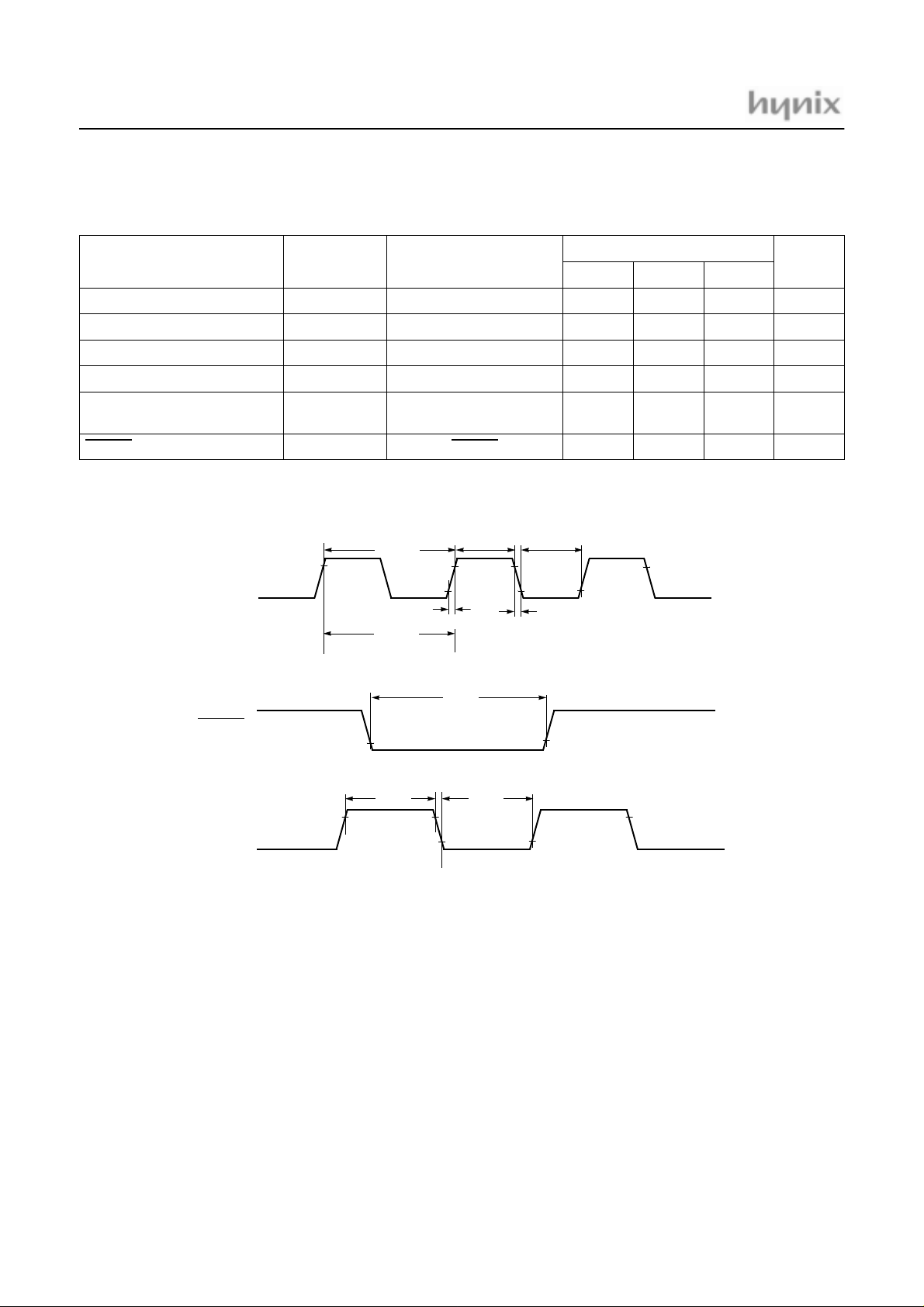
7.5 AC Characteristics
(TA=-20~85°C for GMS81C1404/1408 or TA=-40~85°C for GMS81C1404E/1408E, VDD=5V±10%, VSS=0V)
Parameter Symbol Pins
Operating Frequency
External Clock Pulse Width
External Clock Transition Time
Oscillation Stabilizing Time
External Input Pulse Width
RESET Input Width
X
IN
f
CP
t
CPW
t
RCP,tFCP
t
ST
t
EPW
t
RST
X
IN
X
IN
X
IN
XIN, X
OUT
INT0, INT1, INT2, INT3
EC0, EC1
RESET 8--
t
t
1/f
SYS
CP
t
RCP
t
CPW
RST
t
FCP
t
CPW
Specifications
Unit
Min. Typ. Max.
1-8MHz
80 - - nS
- - 20 nS
--20mS
2--
-0.5V
V
DD
0.5V
t
t
SYS
SYS
RESET
INT0, INT1
INT3
INT2,
EC0,
EC1
t
EPW
t
EPW
Figure 7-1 Timing Chart
0.2V
0.2V
DD
DD
0.8V
DD
14
June. 2001 Ver 1.2
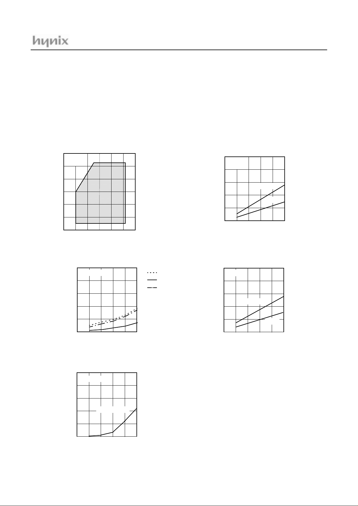
7.6 Typical Characteristics
GMS81C1404/GMS81C1408
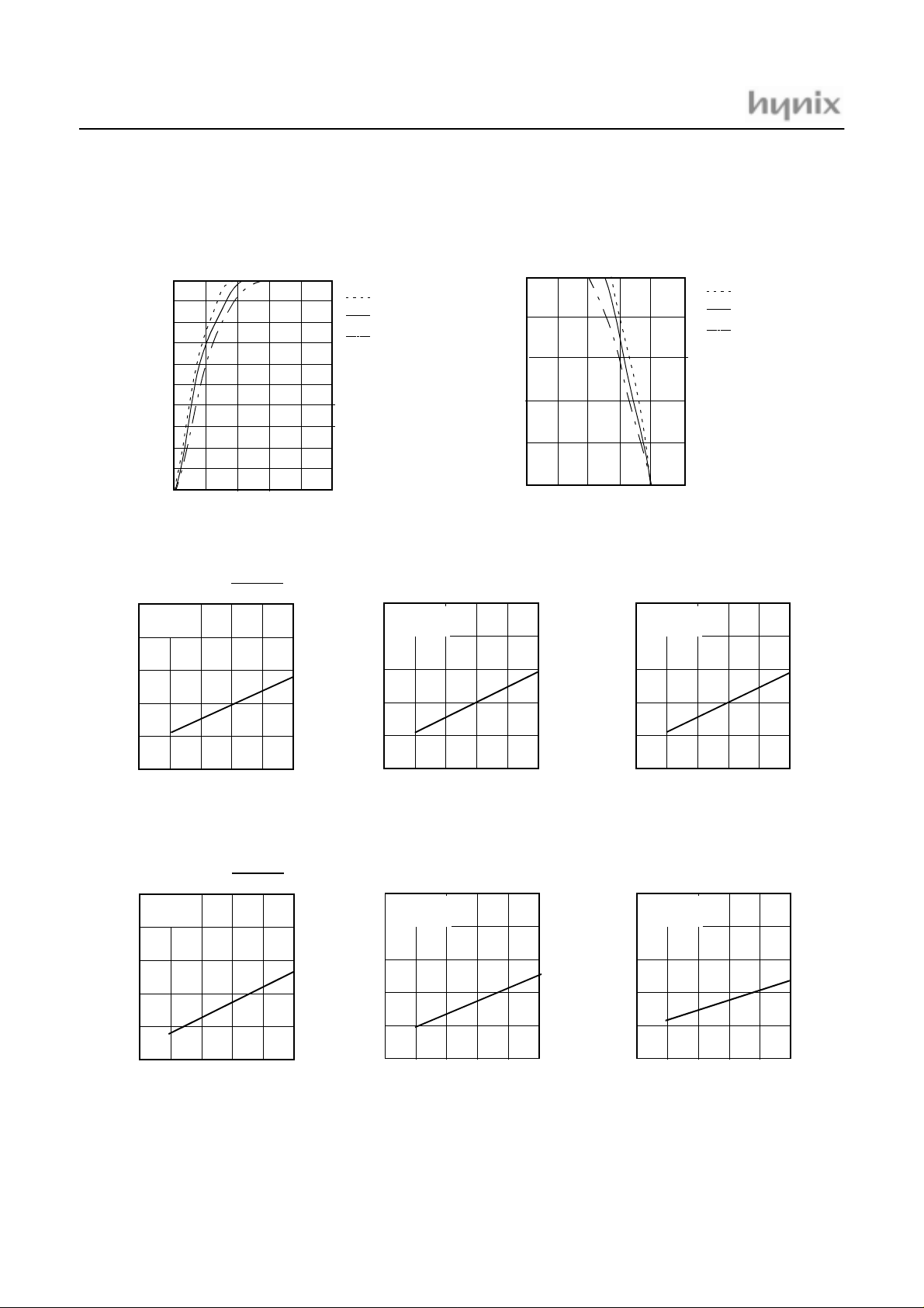
This graphs and tables provided in this section are for design guidance only and are not tested or guaranteed.
In some graphs or tables the data presented are outside specified operating range (e.g. outside specified
VDD range). This is for information only and devices
are guaranteed to operate properly only within the
specified range.
Operating Area
f
XIN
(MHz)
Ta= 25°C
10
8
6
4
2
0
23
45
V
DD
(V)
6
STOP Mode
I
DD
(µA)
I
0.8
0.6
0.4
STOP
f
= 8MHz
XIN
V
−
DD
-40°C
25°C
85°C
The data presented in this s ection is a statistical s ummary
of data collected on units from different lots over a period
of time. “Typical” represents the mean of the distribution
while “max” or “min” represents (mean + 3σ) and (mean −
3σ) respectively where σ is standard deviation
Normal Operation
I
V
−
DD
Ta=25°C
23
DD
f
XIN
= 8MHz
4MHz
45
V
DD
(V)
6
I
DD
(mA)
8
6
4
2
0
Wake-up Timer Mode
I
DD
(mA)
2.0
1.5
1.0
I
WKUP
Ta=25°C
−
f
XIN
V
DD
= 8MHz
0.2
0
23
45
V
DD
(V)
6
0.5
0
23
4MHz
45
V
DD
(V)
6
RC-WDT in Stop Mode
I
DD
(µA)
20
15
10
5
0
I
RCWDT
Ta=25°C
23
V
−
T
RCWDT
DD
= 80uS
45
V
DD
(V)
6
June. 2001 Ver 1.2 15
GMS81C1404/GMS81C1408
I
OL
I
OL
(mA)
40
30
20
10
0
V
V
−
DD
IH1
V
IH1
f
=4MHz
XIN
(V)
Ta=25°C
4
3
2
, VDD=5V
V
−
OL
12345
XIN, RESET
I
OH
I
OH
-40°C
25°C
85°C
V
OL
(V)
V
V
−
DD
IH2
V
IH2
f
=4kHz
XIN
(V)
Ta=25°C
4
3
2
(mA)
-20
-15
-10
-5
0
Hysteresis input
, VDD=5V
V
−
OH
V
23456
V
V
−
DD
IH3
V
IH3
f
=4kHz
XIN
(V)
Ta=25°C
4
3
2
-40°C
OH
(V)
Normal input
25°C
85°C
V
(V)
IL2
1
0
V
4
3
2
1
0
23
V
−
DD
f
=4kHz
XIN
Ta=25°C
23
45
IL2
Hysteresis input
45
V
DD
(V)
6
V
DD
(V)
6
1
0
1
23
V
V
−
DD
V
IL1
f
=4MHz
XIN
(V)
Ta=25°C
4
3
2
1
0
1
23
45
IL1
XIN, RESET
45
V
DD
(V)
6
V
DD
(V)
6
V
(V)
IL3
1
0
V
4
3
2
1
0
23
V
−
DD
f
=4kHz
XIN
Ta=25°C
23
IL3
Normal input
45
45
V
DD
(V)
6
V
DD
(V)
6
16
June. 2001 Ver 1.2

GMS81C1404/GMS81C1408
8. ELECTRICAL CHARACTERISTICS (GMS87C1404/GMS87C1408)
8.1 Absolute Maximum Ratings
Supply voltage...........................................-0.3 to +6.0 V
Storage Temperature ................................-40 to +125 °C
Voltage on any pin with respect to Ground (V
SS
)
................................ ............................... -0.3 to VDD+0.3
Maximum current out of V
Maximum current into V
Maximum current sunk by (I
Maximum output current sourced by (I
pin........................200 mA
SS
pin ..........................150 mA
DD
per I/O Pin) ........25 mA
OL
per I/O Pin)
OH
...............................................................................15 mA
Maximum current (ΣI
) ....................................150 mA
OL
8.2 Recommended Operating Conditions
Maximum current (ΣI
Note: Stresses above those listed under “Absolute Maxi-
mum Ratings” may cause perma nent damage to the
device. This is a stress rat ing only and functional op eration of the device at any other conditions above
those indicated in the operational sections of this
specification is not implied. Exposure to absolute
maximum rating cond itions for extended pe riods
may affect device reliability.
)....................................100 mA
OH
Parameter Symbol Condition
T
V
f
XIN
OPR
DD
Supply Voltage
Operating Frequency
Operating Temperature
8.3 A/D Converter Characteristics
(TA=25°C, VSS=0V, VDD=5.12V @
Parameter Symbol Condition
Analog Input Voltage Range
Analog Power Supply Input Voltage Range
Overall Accuracy
Non-Linearity Error
Differential Non-Linearity Error
Zero Offset Error
Full Scale Error
Gain Error
Conversion Time
AV
Input Current I
REF
f
=8MHz, VDD=3.072V @
XIN
f
=8MHz
XIN
=4.2MHz
f
XIN
VDD=4.5~5.5V
V
=2.5~5.5V
DD
V
AIN
V
REF
N
ACC
N
NLE
N
DNLE
N
ZOE
N
FSE
N
NLE
T
CONV
REF
Specifications
Unit
Min. Max.
4.5 5.5 V
2.5 5.5 V
18MHz
14.2MHz
f
XIN
-20 85
=4MHz)
C
°
Specifications
Unit
Min. Typ. Max.
AVREFS=0
AVREFS=1
VDD=5V
V
=3V
DD
f
=8MHz
XIN
f
=4MHz
XIN
V
SS
V
SS
-
-
3-
2.4 -
-
-
-
-
-
-
±
±
±
±
±
±
1.0
1.0
1.0
0.5
0.25
1.0
--10
--20
V
DD
V
REF
V
DD
V
DD
1.5 LSB
±
1.5 LSB
±
1.5 LSB
±
1.5 LSB
±
0.5 LSB
±
1.5 LSB
±
V
V
V
µ
AVREFS=1 - 0.5 1.0 mA
S
June. 2001 Ver 1.2 17

GMS81C1404/GMS81C1408
8.4 DC Electrical Characteri stics
(TA=-20~85°C, VDD=2.5~5.5V, VSS=0V)
,
Parameter Symbol Pin Condition
XIN, RESET 0.8 V
IH1
Hysteresis Input
IH2
Normal Input
IH3
XIN, RESET
IL1
Hysteresis Input
IL2
Normal Input 0 -
IL3
All Output Port
OH
All Output Port
OL
I
RB2, RB3, RD0, RD1
P
All Pins (except XIN)VDD=5V
IH1
X
IH2
IL1
IL2
T
IN
All Pins (except XIN)VDD=5V
X
IN
|
Hysteresis Input
1
1
VDD=5V, IOH=-5mA VDD -1
VDD=5V, IOL=10mA
VDD=5V
VDD=5V
VDD=5V
1
VDD=5V
PFD Level = 0 2.5 3.0 3.5
PFD Level = 1 2.0 2.5 3.0
VDD=5V
V
DD
Input High Voltage
Input Low Voltage
Output High Voltage
Output Low Voltage
Input Pull-up Current
Input High
Leakage Current
Input Low
Leakage Current
Hysteresis
PFD Voltage
Internal RC WDT
Period
V
V
V
V
V
V
V
V
I
I
I
I
| V
V
PFD1VDD
V
PFD2VDD
T
RCWDT
VDD=5.5V, f
Operating Current
Wake-up Timer
Mode Current
RCWDT Mode
Current at STOP
Mode
I
I
WKUPVDD
I
RCWDTVDD
DD
V
DD
V
DD
VDD=5.5V, f
V
DD
VDD=5.5V
V
DD
VDD=5.5V, f
Stop Mode Current
1. Hysteresis Input: RB2, RB3, RB6, RC3, RC4, RC5, RD0, RD1
I
STOP
V
DD
V
DD
=3V
=3.0V, f
=3.0V, f
=3.0V
=3.0V, f
XIN
XIN
XIN
XIN
XIN
XIN
=8MHz
=4MHz
=8MHz
=4MHz
=8MHz
=4MHz
Specifications
Min. Typ. Max.
-
-
-
0.8 V
0.7 V
DD
DD
DD
00-
V
V
V
0.2 V
0.2 V
0.3 V
DD
DD
DD
DD
DD
DD
--V
-
-1V
-550 -420 -200
--5µA
--15µA
-5 - -
-15 - -
0.5 - - V
40 120
95 280
-56
-23
-12
-0.51
--200
--100
-0.53
-0.21
Unit
V
V
A
µ
A
µ
A
µ
V
S
µ
mA
mA
A
µ
A
µ
18
June. 2001 Ver 1.2
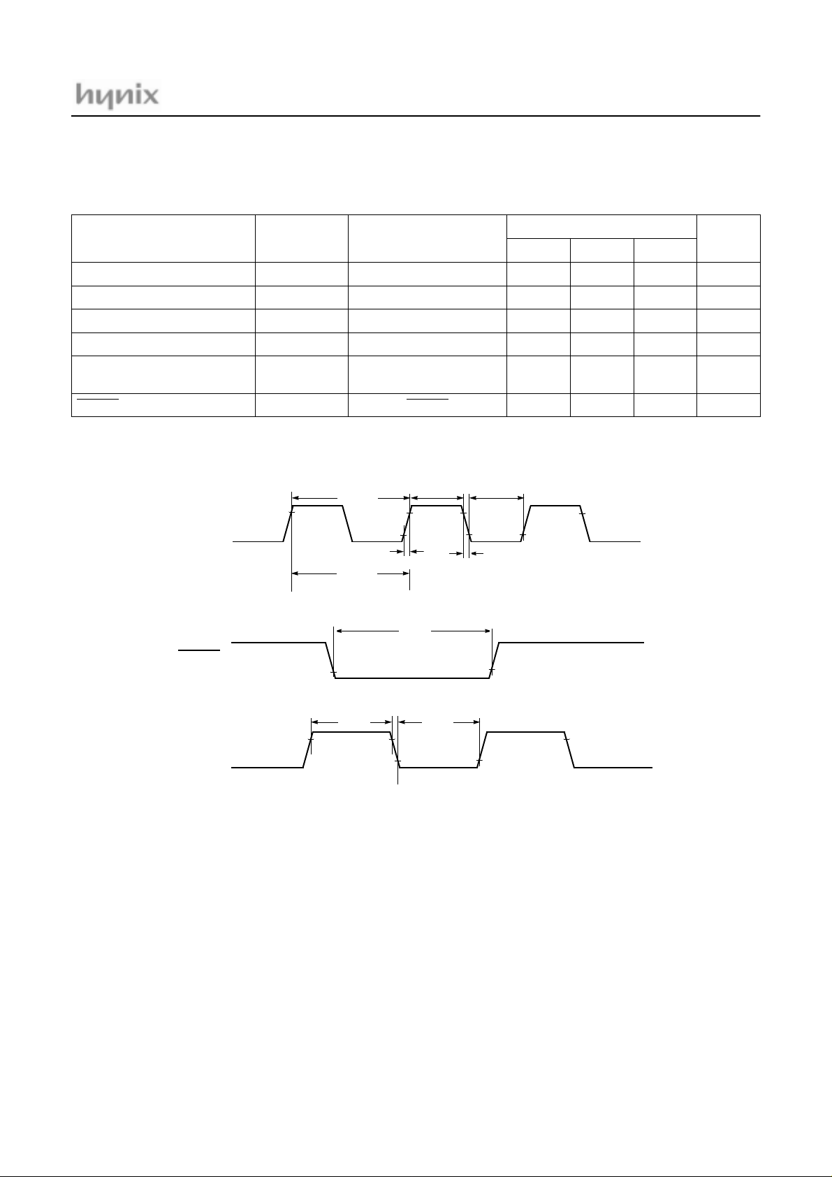
8.5 AC Characteristics
(TA=-20~+85°C, VDD=5V±10%, VSS=0V)
GMS81C1404/GMS81C1408
Parameter Symbol Pins
Operating Frequency
External Clock Pulse Width
External Clock Transition Time
Oscillation Stabilizing Time
External Input Pulse Width
RESET Input Width
X
IN
f
CP
t
CPW
t
RCP,tFCP
t
ST
t
EPW
t
RST
X
IN
X
IN
X
IN
XIN, X
OUT
INT0, INT1, INT2, INT3
EC0, EC1
RESET 8--
t
t
1/f
SYS
CP
t
RCP
t
CPW
RST
t
FCP
t
CPW
Specifications
Unit
Min. Typ. Max.
1-8MHz
80 - - nS
- - 20 nS
--20mS
2--
-0.5V
V
DD
0.5V
t
t
SYS
SYS
RESET
INT0, INT1
INT3
INT2,
EC0,
EC1
t
EPW
t
EPW
Figure 8-1 Timing Chart
0.2V
0.2V
DD
DD
0.8V
DD
June. 2001 Ver 1.2 19
GMS81C1404/GMS81C1408
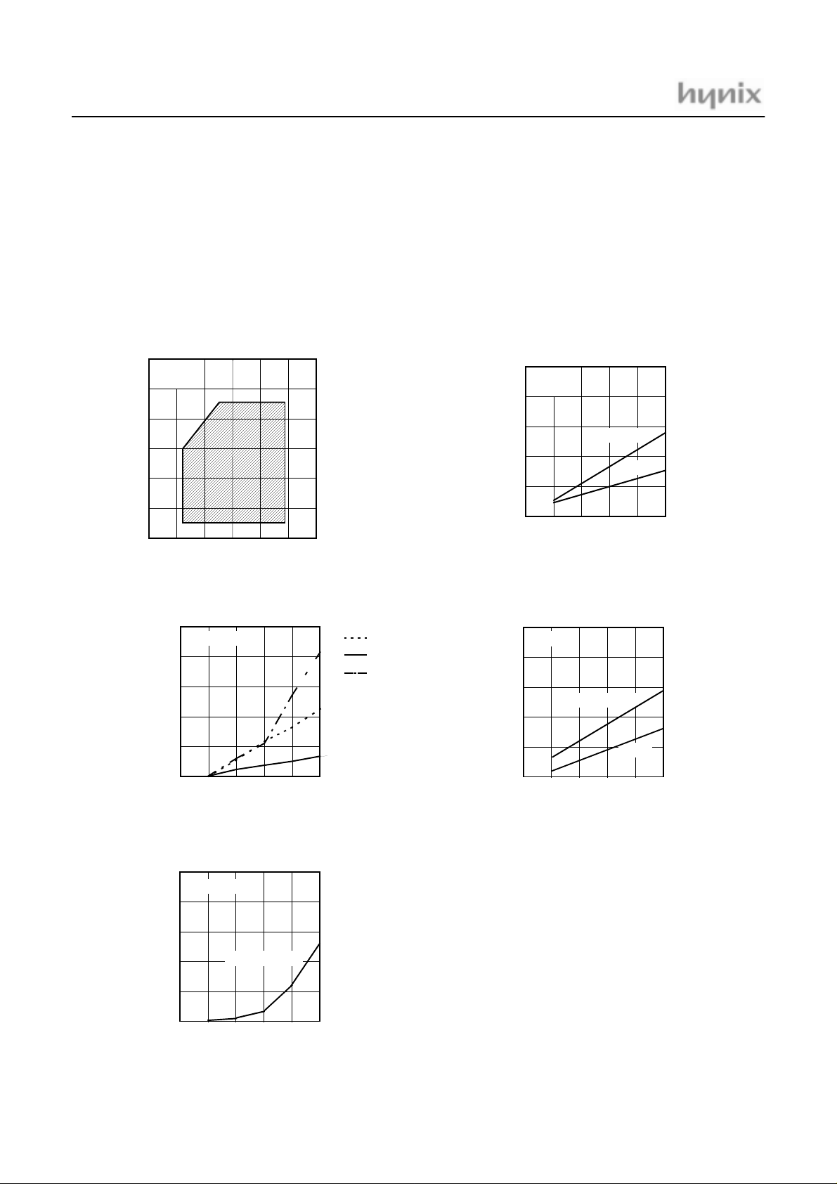
8.6 Typical Characteristics
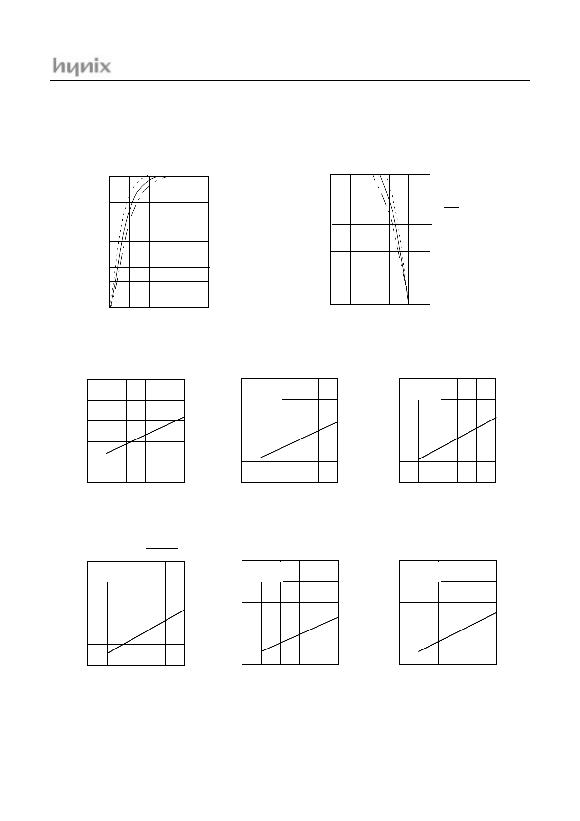
This graphs and tables provided in this section are for design guidance only and are not tested or guaranteed.
In some graphs or tables the data presented are outside specified operating range (e.g. outside specified
VDD range). This is for information only and devices
are guaranteed to operate properly only within the
specified range.
Operating Area
f
XIN
(MHz)
Ta= 25°C
10
8
6
4
2
0
23
45
V
DD
(V)
6
STOP Mode
I
DD
(µA)
I
0.8
0.6
0.4
STOP
f
= 8MHz
XIN
V
−
DD
-25°C
25°C
85°C
The data presented in this s ection is a statistical s ummary
of data collected on units from different lots over a period
of time. “Typical” represents the mean of the distribution
while “max” or “min” represents (mean + 3σ) and (mean −
3σ) respectively where σ is standard deviation
Normal Operation
I
V
−
DD
Ta=25°C
23
DD
f
XIN
= 8MHz
4MHz
45
V
DD
(V)
6
I
DD
(mA)
8
6
4
2
0
Wake-up Timer Mode
I
DD
(mA)
2.0
1.5
1.0
I
WKUP
Ta=25°C
V
−
DD
f
= 8MHz
XIN
20
0.2
0
23
RC-WDT in Stop Mode
I
DD
(µA)
20
15
10
5
0
I
RCWDT
Ta=25°C
23
V
−
T
RCWDT
DD
45
= 80uS
45
0.5
V
DD
(V)
6
V
DD
(V)
6
0
23
4MHz
V
DD
(V)
45
6
June. 2001 Ver 1.2
GMS81C1404/GMS81C1408
I
OL
I
OL
(mA)
40
30
20
10
0
V
V
−
DD
IH1
V
IH1
f
=4MHz
XIN
(V)
Ta=25°C
4
3
2
, VDD=5V
V
−
OL
12345
XIN, RESET
I
OH
I
OH
-25°C
25°C
85°C
V
OL
(V)
V
V
−
DD
IH2
V
IH2
f
=4kHz
XIN
(V)
Ta=25°C
4
3
2
(mA)
-20
-15
-10
-5
0
Hysteresis input
, VDD=5V
V
−
OH
V
23456
V
V
−
DD
IH3
V
IH3
f
=4kHz
XIN
(V)
Ta=25°C
4
3
2
-25°C
OH
(V)
Normal input
25°C
85°C
V
(V)
IL2
1
0
V
4
3
2
1
0
23
V
−
DD
f
=4kHz
XIN
Ta=25°C
23
45
IL2
Hysteresis input
45
V
DD
(V)
6
V
DD
(V)
6
1
0
1
23
V
V
−
DD
V
IL1
f
=4MHz
XIN
(V)
Ta=25°C
4
3
2
1
0
1
23
45
IL1
XIN, RESET
45
V
DD
(V)
6
V
DD
(V)
6
V
(V)
IL3
1
0
V
4
3
2
1
0
23
V
−
DD
f
=4kHz
XIN
Ta=25°C
23
IL3
Normal input
45
45
V
DD
(V)
6
V
DD
(V)
6
June. 2001 Ver 1.2 21

GMS81C1404/GMS81C1408
9. MEMORY ORGANIZATION
The GMS81C1404 and GMS81C1408 have separate address spaces for Program memory and Data Memory. Pro gram memory can only be read, not written to. It can be up
9.1 Registers
This device has six registers that are the Program Counter
(PC), a Accumulator (A), two index registers (X, Y), the
Stack Pointer (SP), and the Program Status Word (PSW).
The Program Counter consists of 16-bit register.
A
X
Y
SP
PCLPCH
PSW
Figure 9-1 Configuration of Registers
Accumulator: The Accumulato r is the 8-bit gen eral purpose register, used for data operation such as transfer, temporary saving, and conditional judgement, etc.
The Accumulator can be used as a 16-bit register with Y
Register as shown below.
ACCUMULATOR
X REGISTER
Y REGISTER
STACK POINTER
PROGRAM COUNTER
PROGRAM STATUS
WORD
to 4K /8K bytes of Prog ram memor y. Data memory ca n be
read and written to up to 192 bytes including the stack area.
Generally, SP is automatically updated when a subrout ine
call is executed or an interrupt is accepted. However, if it
is used in excess of the stack area permitted by the data
memory allocating configuration, the us er-processed data
may be lost.
The stack can be located at any position within 00
to BF
H
of the internal data memory. The SP is not initialized by
hardware, requiring to write the initial value (the location
with which the use of the stack starts) by using the initialization routine. Normally, the initial value of “BF
H
” is
used.
Stack Address (000
15 087
0
Hardware fixed
The Stack Pointer must be initi alized by softwa re be-
Note:
cause its value is undefined after RESET.
Example: To initialize the SP
LDX #0BFH
TXSP ; SP ← BFH
~ 0BFH)
H
SP
H
Y
Y A
A
Two 8-bit Registers can be used as a “YA” 16-bit Register
Figure 9-2 Configuration of YA 16 -bit Register
X, Y Registers: In the addressing mode which uses these
index registers, the register conten ts a re added to the specified address, which becomes the actual address. These
modes are extremely effective for referencing subroutine
tables and memory tables . The index regi sters also h ave increment, decrement, comparison and data transfer functions, and they can be used as simple accumulators.
Stack Pointer: The Stack Pointer is an 8-bit register used
for occurrence interrupts and calling out subroutines. Stack
Pointer identifies the location in the stack to be accessed
(save or restore).
22
Program Counter: The Program Counter is a 16-bit wide
which consists of two 8-bit regist ers, PCH and PCL. This
counter indicates the address of the next instruction to be
executed. In reset state, the program counter has reset routine address (PC
:0FFH, PCL:0FEH).
H
Program Status Word: The Program Status Word (PSW)
contains several bits that reflect the current state of the
CPU. The PSW is described in Figure 9-3 . It contains the
Negative flag, the Overflow flag, the Break flag the Half
Carry (for BCD operation), the Interrupt enable flag, the
Zero flag, and the Carry flag.
[Carry flag C]
This flag stores any carry or borrow from the ALU of CPU
after an arithmetic operation and is also changed by the
Shift Instruction or Rotate Instruction.
[Zero flag Z]
This flag is set when the result of an arithmetic operation
or data transfer is “0” and is cleared by any other result.
June. 2001 Ver 1.2

PSW
MSB LSB
N
V - B H I Z C
RESET VALUE: 00
GMS81C1404/GMS81C1408
H
NEGATIVE FLAG
OVERFLOW FLAG
BRK FLAG
Figure 9-3 PSW (Program Status Word) Register
[Interrupt disable flag I]
This flag enables/disables all interrupts except interrupt
caused by Reset or software BRK instruction. All interrupts are disabled when cleared to “0”. This flag immediately becomes “0” when an interrupt is served. It is set by
the EI instruction and cleared by the DI instruction.
[Half carry flag H]
After operation, this is set when there is a carry from bit 3
of ALU or there is no borrow from bit 4 of ALU. This bit
can not be set or cleared except CLRV instruction with
Overflow flag (V).
[Break flag B]
This flag is set by software BRK instruction to distinguish
BRK from TCALL instruction with the same vector ad-
CARRY FLAG RECEIVES
CARRY OUT
ZERO FLAG
INTERRUPT ENABLE FLAG
HALF CARRY FLAG RECEIVES
CARRY OUT FROM BIT 1 OF
ADDITION OPERLANDS
dress.
[Overflow flag V]
This flag is set to “1” when an overflow occurs as the result
of an arithmetic operation involving signs. An overflow
occurs when the result of an addition or subtraction exceeds +127(7F
) or -128(80H). The CLRV instruction
H
clears the overflow flag. There is no set instruction. When
the BIT instruction is executed, bit 6 of memory is copied
to this flag.
[Negative flag N]
This flag is set to match the sign bit (bit 7) status of the re-
sult of a data or arithmetic operation. When the BIT instruction is executed, bit 7 of memory is copied to this flag.
June. 2001 Ver 1.2 23

GMS81C1404/GMS81C1408
9.2 Program Memory
A 16-bit program counter is capable of addressing up to
64K bytes, but these devices have 4K/8K bytes program
memory space only physically implemented. Accessing a
location above FFFF
will cause a wrap-around to 0000H.
H
Figure 9-4 , shows a map of Progr am Memory. After reset ,
the CPU begins execution from reset vector which is stored
in address FFFE
and FFFFH as shown in Figure 9-5 .
H
As shown in Figure 9-4 , each area is assigned a fixed location in Program M emory. Program Memory area contains the user program.
E000H
GMS81C1408
F000H
GMS81C1404
FEFFH
FF00H
FFC0H
FFDFH
FFE0H
FFFFH
TCALL
AREA
INTERRUPT
VECTOR AREA
PROGRAM
MEMORY
PCALL
AREA
Example: Usage of TCALL
LDA #5
TCALL 0FH ;
:;
:;
;
;TABLE CALL ROUTINE
;
FUNC_A: LDA LRG0
RET
;
FUNC_B: LDA LRG1
RET
;
;TABLE CALL ADD. AREA
;
ORG 0FFC0H ;
DW FUNC_A
DW FUNC_B
1BYTE INSTRUCTION
INSTEAD O F 3 BYTES
NORMAL CALL
1
2
TCALL ADDRESS AREA
The interrupt causes the CPU to jum p to specific location,
where it commences the execution of the service routine.
The External interrupt 0, for example, is assigned to location 0FFFA
interval: 0FFF8
0FFFA
As for the area from 0FF00
. The interrupt service locations spaces 2-byte
H
and 0FFF9H for External Interru pt 1,
H
and 0FFFBH for External Interrupt 0, etc.
H
to 0FFFFH, if any area of
H
them is not going to be used, its s ervice location is available as general purpose Program Memory.
Figure 9-4 Program Memory Map
Page Call (PCALL) area contains subroutine program to
reduce program byte length by using 2 bytes PCALL instead of 3 bytes CALL instruction. If it is frequently called,
it is more useful to save program byte length .
Table Call (TCALL) c auses the CPU to jump to each
TCALL address, where it commences the execution of the
service routine. The Table Call service area spaces 2-byte
for every TCALL: 0FFC0
for TCALL15, 0FFC2H for
H
TCALL14, etc., as shown in Figure 9-6 .
Address Vector Area Memory
0FFE0
H
E2
E4
Serial Peripheral Interface Interrupt Vector Area
E6
E8
EA
EC
EE
F0
F2
F4
F6
F8
FA
FC
FE
NOTE:
“-” means reserved area.
Basic Interval Interrupt Vector Area
Watchdog Timer Interru pt Ve ctor Area
A/D Converter Interrupt Vector Area
Timer/Counter 3 Interrupt Vector Area
Timer/Counter 2 Interrupt Vector Area
External Interrupt 3 Vector Area
External Interrupt 2 Vector Area
Timer/Counter 1 Interrupt Vector Area
Timer/Counter 0 Interrupt Vector Area
External Interrupt 1 Vector Area
External Interrupt 0 Vector Area
RESET Vector Area
-
-
-
Figure 9-5 Interrupt Vector Area
24
June. 2001 Ver 1.2

Address PCALL Area Memory
0FF00
H
PCALL Area
(256 Bytes)
0FFFF
H
GMS81C1404/GMS81C1408
Address Program Memory
0FFC0
H
C1
C2
C3
C4
C5
C6
C7
C8
C9
CA
CB
CC
CD
CE
CF
D0
D1
D2
D3
D4
D5
D6
D7
D8
D9
DA
DB
DC
DD
DE
DF
NOTE:
* means that the BRK software interrupt is using
same address with TCALL0.
TCALL 15
TCALL 14
TCALL 13
TCALL 12
TCALL 11
TCALL 10
TCALL 9
TCALL 8
TCALL 7
TCALL 6
TCALL 5
TCALL 4
TCALL 3
TCALL 2
TCALL 1
TCALL 0 / BRK *
Figure 9-6 PCALL and TCALL Memory Area
PCALL→ rel
4F35 PCALL 35H
~
~
0FF00H
0FF35H
0FFFFH
4F
35
NEXT
~
~
TCALL→ n
4A TCALL 4
4A
~
~
0F125H
0FF00H
0FFD6H
0FFD7H
0FFFFH
NEXT
25
F1
01001010
~
~
PC:
11111111
FHFHDH6
➌
Reverse
➊
11010110
➋
H
June. 2001 Ver 1.2 25

GMS81C1404/GMS81C1408
Example: The usage software example of Vector address and the initialize part.
ORG 0FFE0H
DW NOT_USED ; (0FFEO)
DW NOT_USED ; (0FFE2)
DW SPI_INT ; (0FFE4) Serial Peripheral Interface
DW BIT_INT ; (0FFE6) Basic Interval Timer
DW WDT_INT ; (0FFE8) Watchdog Timer
DW AD_INT ; (0FFEA) A/D
DW TMR3_INT ; (0FFEC) Timer-3
DW TMR2_INT ; (0FFEE) Timer-2
DW INT3 ; (0FFF0) Int.3
DW INT2 ; (0FFF2) Int.2
DW TMR1_INT ; (0FFF4) Timer-1
DW TMR0_INT ; (0FFF6) Timer-0
DW INT1 ; (0FFF8) Int.1
DW INT0 ; (0FFFA) Int.0
DW NOT_USED ; (0FFFC)
DW RESET ; (0FFFE) Reset
ORG 0F000H
;********************************************
; MAIN PROGRAM *
;*******************************************
;
RESET: DI ;Disable All Interrupts
RAM_CLR: LDA #0 ;RAM Clear(!0000H->!00BFH)
;
;
;
LDX #0
STA {X}+
CMPX #0C0H
BNE RAM_CLR
LDX #0BFH ;Stack Pointer Initialize
TXSP
CALL INITIAL ;
LDM RA, #0 ;Normal Port A
LDM RAIO,#1000_0010B ;Normal Port Direction
LDM RB, #0 ;Normal Port B
LDM RBIO,#1000_0010B ;Normal Port Direction
:
:
LDM PFDR,#0 ;Enable Power Fail Detector
:
:
26
June. 2001 Ver 1.2
 Loading...