HYNIX GMS81C7016Q, GMS81C7016K, GMS81C7016, GMS81C7008Q, GMS81C7008K Datasheet
...
HYNIX SEMICONDUCTOR INC.
8-BIT SINGLE-CHIP MICROCONTROLLERS
GMS81C7008
GMS81C7016
User’s Manual
(Ver. 2.01)

Version 2.01
Published by
MCU Application Team
2001 Hynix semiconductor Inc. All right reserved.
Additional inf orm ati on of this man ual m ay be serv ed by Hyni x sem ico nduc tor offic es in Ko rea o r Dis tri butor s and Rep rese nta tives listed
at address directory.
Hynix semiconductor reserves the right to make changes to any information here in at any ti m e without notice.
The information, diagrams and other data in this manual are correct and reliable; however, Hynix semiconductor is in no way responsible
for any violations of patents or other rights of the third party generated by the use of this manual.
REVISION HISTORY
VERSION 2.01 (APR., 2001) This book
Delete product of 52SDIP package also , no longer produce 52 pi n MC U .
The compay name Hyundai Electronics Industires Co., Ltd. changed to Hynix Semiconductor Inc.
VERSION 2.00 (FEB., 2001)
Delete product of 52LQFP package.
Fixed some errata that pin number 25 and 26 on 52SDIP package are reversed.
VERSION 1.02 (NOV., 2000)
Fixed the name of LCR r e gister on page 39 and 75, the BUR register on page 66.
VERSION 1.01 (SEP., 2000) sticker
Correct the bit LVDE of LVDR register on page 91.

GMS81C7008/7016/7108/7116
APR., 2001 Ver 2.01
Table of Contents
1. OVERVIEW............................................1
Description .........................................................1
Features ............................... ..............................1
Development Tools ............................................2
Ordering Information ..........................................2
2. BLOCK DIAGRAM.................................3
3. PIN ASSIGNMENT ................................4
4. PACKAGE DIMENSION ........................5
5. PIN FUNCTION......................................6
6. PORT STRUCTURES............................9
7. ELECTRICAL CHARACTERISTICS....11
Absolute Maximum Ratings .............................11
Recommended Operating Conditions ..............11
DC Electrical Characteristics ............ ...... ....... ..1 1
A/D Converter Characteristics .........................13
AC Characteristics ...........................................13
Serial Interface Timing Characteristics ............15
Typical Characteristics .....................................16
8. MEMORY ORGANIZATION.................18
Registers ....................... ...................................18
Program Memory ....................... ....... ...............21
Data Memory ...................................................24
List of Control Registers ...................................25
Addressing Mode .............................................28
9. I/O PORTS...........................................32
Registers for Port .............................................32
I/O Ports Configuration ....................................33
10. CLOCK GENERATOR.......................37
11. OPERATION MODE..........................39
Operation Mode Switching ...............................40
12. BASIC INTERVAL TIMER..................42
13. TIMER/EVENT COUNTER................44
8-bit Timer / Counter Mode ..............................47
16-bit Timer / Counter Mode ............................51
8-bit Capture Mode ..........................................52
16-bit Capture Mode .................. ....... ...... ....... ..5 3
Timer output port mode ....................................53
PWM Mode ......................................................54
14. ANALOG DIGITAL CONVERTER.....57
15. SERIAL COMMUNICATION..............59
Transmission/Recei vi ng Timi ng ........... ........... 60
The method of Serial I/O ................................. 61
The Method to Test Correct Transmission ...... 61
16. BUZZER FUNCTION.........................62
17. INTERRUPTS....................................64
Interrupt Sequence .......................................... 66
BRK Interrupt .................................................. 67
Multi Interrupt .................................................. 67
External Interrupt ............................................. 68
Key Scan Interrupt .......................................... 68
18. LCD DRIVER..................................... 70
LCD Control Registers .................................... 70
Duty and Bias Selection of LCD driver ............ 72
Selecting Frame Frequency ............................ 72
LCD Display Memory ...................................... 75
Control Method of LCD Driver ......................... 76
19. WATCH / WATCHDOG TIMER.........78
Watch Timer ............................ ...... .................. 78
Watchdog Timer ...................... ...... ....... ........... 78
20. POWER DOWN OPERATION...........81
SLEEP Mode ................................................... 81
STOP Mode .................................................... 82
21. OSCILLATOR CIRCUIT.....................85
22. RESET...............................................86
External Reset Input ........................................ 86
Watchdog Timer Reset ................................... 86
23. POWER FAIL PROCESSOR.............87
24. DEVELOPMENT TOOLS...................89
OTP Programming .......................................... 89
Emulator EVA. Board Setting .......................... 90
Appendix
A. MASK ORDER SHEET ..........................i
B. INSTRUCTION......... ..... ..... ...................ii
Terminology List .................................................ii
Instruction Map ..................................................iii

GMS81C7008/7016/7108/7116
APR., 2001 Ver 2.01
Instruction Set ...................................................iv
C. SOFTWARE EXAMPLE........................x

GMS81C7008/7016
APR., 2001 Ver 2.01 1
GMS81C7008/16
CMOS SINGLE-CHIP 8-BIT MICROCONTROLLER
WITH LCD DRIVER & A/D CONVERTER
1. OVERVIEW
1.1 Description
The GMS81C7008/ 7016 is advanc ed CMOS 8-bit micro controlle rs with 8K/16K by tes of ROM. There are a po werful microc ontroller
which provides a high ly flexible and cost effective solution to many LCD applicatio ns. These p rovide th e following standard fe atures:16K/
8K bytes of mask type ROM or 16K bytes OTP ROM, 448 bytes of RAM, 8-bit timer/counter, 8-bit A/D converter, 10 bit high speed PWM
Output, programmabl e buzzer d riving p ort, 8-bi t basic i nterval t imer, wat ch dog t imer, serial peri pheral in terface, on chip o sc illator and
clock circuitry. They also come with 4com/24seg LCD driver. In addition, it suppo rt power saving mode to re duce power consumption.
1.2 Features
• 8K/16K Bytes On-chip Programmable ROM
• 448 Bytes of On-chip Data RAM
(Included stack area and 27 nibbles LCD Display
RAM)
• Instruction Execution Time
1µs at 4MHz (2cycle NOP In struction)
• One 8-bit Basic Interval Timer
• One Watch Timer
• One Watchdog Timer
• Four 8-bit Timer/Event Counter
(or Two 16-bit Timer/Event Counter)
• Two channel 10-bit High Speed PWM Output
• Three External Interrupt input ports
• One Programmable 6-bit Buzzer Driving port
- 500Hz ~ 250kHz@4MHz
• 49 I/O Ports
• Eight channel 8-bit A/D converter
• One 8-bit Serial Communication Interface
• LCD Display/ Controller
- Static Mode (27SEG x 1COM, Static)
- 1/2 Duty Mode (26SEG x 2COM, 1/2 or 1/3 Bias)
- 1/3 Duty Mode (25SEG x 3COM, 1/3 Bias)
- 1/4 Duty Mode (24SEG x 4COM, 1/3 Bias)
- Internal Built-in Resistor Circuit for Bias
• Thirteen Interrupt sources
- Basic Interval Timer: 1
- External input: 3
- Timer/Event counter: 4
- ADC: 1
- Serial Interface: 1
- WT:1
- WDT: 1
- Key Scan: 1
• Main Clock Oscillation (1.0~4.5MHz)
- Crystal
- Ceramic Resonator
- External R Oscillator (Built-in Capacitor)
• Sub Clock Oscillation
- 32.768kHz Crystal Oscillator
• Power Saving Operation Mode
- Main / Sub Active mode changeable
- 2/8/16/64 divided system clock selectable
• Power Down Mode
- STOP mode
- SLEEP mode
- Sub active Mode
• 2.7V to 5.5V Wide Operating Voltage Range
• Noise Immunity Circuit for EMS
Device name ROM Size RAM Size I/O OTP Package
GMS81C7008 8K bytes 448 bytes 49 GMS87C7016
64SDIP, 64MQFP
GMS81C7016 16K bytes 448 bytes 49 GMS87C7016
GMS81C7008/7016
2 APR., 2001 Ver 2.01
- Power fail processor
- Built in Noise filter
• 64SDIP, 64LQFP package types
• Available 16K bytes OTP version
1.3 Development Tools
Note: There are several setting switches in the Emulator.
User should read carefully and do setting properly before
developing the prog ram refer to " 24.2 Emul ator EVA. Board
Setting" on page 90. Otherw ise, the Emulator ma y not work
properly.
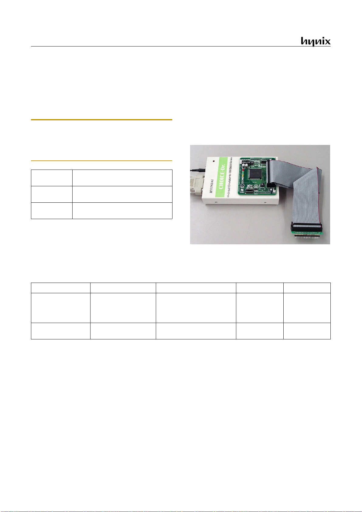
The GMS81C7008/16 is supported by a full-featured macro assembler, an in-circuit emulator CHOICE-Dr.
TM
and OTP programmers. There are two different type programmers, one is
single type, another is gang type. For more detail, refer to OTP
Programming chapt er. Ma cro as sembler ope rat es unde r the MS-
Windows 95/98TM.
Please contact sales part of Hynix semiconductor.
1.4 Ordering Information
Software
- MS- Window base assembler
- Linker / Editor / Debugger
Hardware
(Emulator)
- CHOICE-Dr.
- CHOICE-Dr. EVA 81C51/81C7X B/D
OTP programmer
- CHOICE-SIGMA (Single type)
- CHOICE-GANG4 (4-gang type)
Device na me ROM Size (bytes) RAM size Package
Mask ROM version
GMS81C7008 K
GMS81C7016 K
GMS81C7008 Q
GMS81C7016 Q
8K bytes
16K bytes
8K bytes
16K bytes
448 bytes
448 bytes
448 bytes
448 bytes
64SDIP
64SDIP
64MQFP
64MQFP
OTP ROM version
GMS87C7016 K
GMS87C7016 Q
16K bytes OTP
16K bytes OTP
448 bytes
448 bytes
64SDIP
64MQFP
GMS81C7008/7016
APR., 2001 Ver 2.01 3
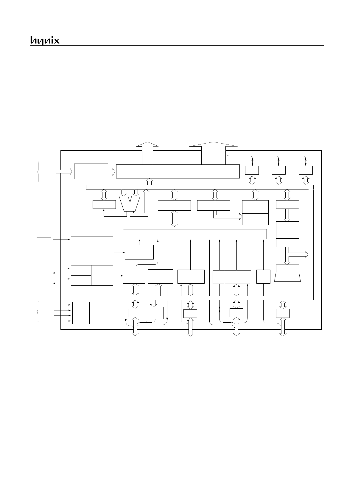
2. BLOCK DIAGRAM
GMS81C7008/7016
ALU
LCD Controller / Driver (LCDC)
Accumulator Stack Pointer
Interrupt Controller
Data
Memory
LCD Display
Memory
Program
Memory
Data Table
PC
8-bit Basic
Interv a l T imer
High Speed
PC
R1
R0
R3
Buzzer
Driver
PSW
System controller
Timing generator
System
Clock Controller
Clock
Generator
High freq.
Low freq.
RESET
XIN
XOUT
SXIN
SXOUT
Common Drive Output
COM0
R00 / INT0
R01 / INT1
R02 / INT2
R03 / EC0
R04 / EC2
R05 / SCK
R06 / SO
R07 / SI
R10
R11
R30 / BUZ
VDD
VSS
Power
Supply
VCL0
VCL1
VCL2
COM1/SEG26
COM2/SEG25
COM3/SEG24
LCD Power
Control Circuit
AVDD
AVSS
Power
Supply
Circuit
BIAS
R20 / AN0
R31 / PWM0 / T1O
R32 / PWM1 / T3O
R33
R21 / AN1
R22 / AN2
R23 / AN3
8-bit
A/D Converter
R2
PWM
8-bit
Timer/Counter
SIO
R24 / AN4
R25 / AN5
R26 / AN6
R27 / AN7
R4 R5 R6
R34 / WDTO
Watch/
Timer
R35 / SXOUT
R36 / SXIN
Segment Drive Output
SEG0 ~ SEG23
R40-R47
Watchdog
Key
Scan
R50-R56
R60-R67
LCD Power
Supply
GMS81C7008/7016
4 APR., 2001 Ver 2.01
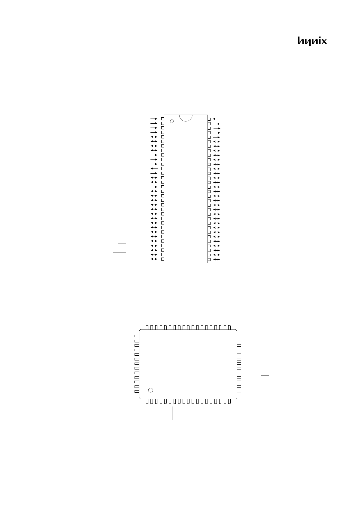
3. PIN ASSIGNMENT
VCL0
VCL1
VCL2
AV
DD
R20
R21
R22
R23
AV
SS
BIAS
X
IN
X
OUT
RESET
R36
R35
V
SS
AN0
AN1
AN2
AN3
PWM1 / T3O
PWM0 / T1O
BUZ
WDTO
R24
R25
R26
R27
R07
R06
R05
R04
R03
R02
R01
R00
R11
R10
R34
R33
SI
SO
EC2
EC0
INT2
INT1
INT0
V
DD
COM3
COM2
COM1
COM0
R67
R66
R65
R64
R63
R62
R61
R60
R57
R56
R55
R54
R53
R52
R51
R50
R47
R46
R45
R44
R43
R42
R41
R40
R30
R31
R32
R21
R66
R67
COM0
COM1
COM2
COM3
V
DD
VCL0
VCL1
VCL2
AV
DD
R20
AN1
SEG22
R02
R42
R41
R40
R30
R31
R32
R33
R34
R10
R11
R00
R01
INT2
INT0
INT1
R65
R63
R62
R61
R60
R57
R56
R55
R54
R53
R52
R51
R50
R47
R46
R45
R64
R44
R43
R22
AV
SS
BIAS
XIN
XOUT
RESET
R36
R35
VSSR24
R25
R26
R27
R07
R06
R05
R23
R04
R03
AN2
SX
IN
SX
OUT
AN4
AN5
AN6
AN7
SI
SO
SCK
AN3
EC2
EC0
123456789
101112131415161718
19
484746
45
4443424140
39
3837363534
33
515049
32
31
30
29
28
27
26
25
24
23
22
21
20
52
53
54
55
56
57
58
59
60
61
62
63
64
64MQFP
64SDIP
1
2
3
4
5
6
7
8
9
10
11
12
13
14
15
16
17
18
19
20
21
22
23
24
25
26
27
28
29
30
31
32
64
63
62
61
60
59
58
57
56
55
54
53
52
51
50
49
48
47
46
45
44
43
42
41
40
39
38
37
36
35
34
33
GMS81C7008/7016
GMS81C7008/7016
(Top View)
(Top View)
AN4
AN5
AN6
AN7
SX
IN
SX
OUT
SCK
SEG0
SEG1
SEG2
SEG3
SEG4
SEG5
SEG6
SEG7
SEG8
SEG9
SEG10
SEG11
SEG12
SEG13
SEG14
SEG15
SEG16
SEG17
SEG18
SEG19
SEG20
SEG21
SEG22
SEG23
SEG26
SEG25
SEG24
WDTO
PWM1/T3O
PWM0/T1O
BUZ
SEG0
SEG1
SEG2
SEG3
SEG4
SEG5
SEG6
SEG7
SEG8
SEG9
SEG10
SEG11
SEG12
SEG13
SEG14
SEG15
SEG16
SEG17
SEG18
SEG19
SEG20
SEG21
SEG23
AN0
SEG26
SEG25
SEG24
KS1
KS0
KS0
KS1
GMS81C7008/7016
APR., 2001 Ver 2.01 5
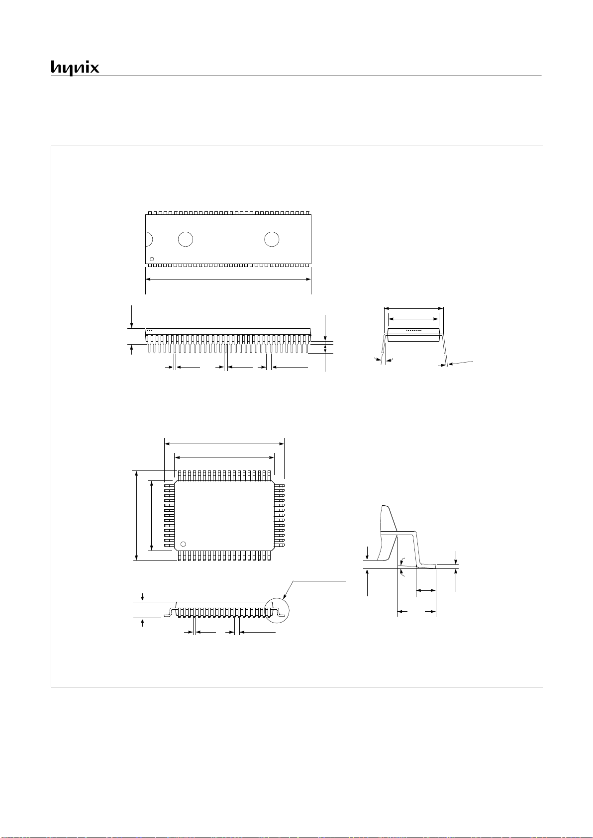
4. PACKAGE DIMENSION
UNIT: INCH
2.280
2.260
0.022
0.016
0.050
0.030
0.070 Typ.
0.140
0.120
min. 0.015
0.680
0.660
0.750 Typ.
0-15
°
64SDIP
0
.0
1
2
0
.0
0
8
0.205 max.
20.10
19.90
24.15
23.65
18.15
17.65
14.10
13.90
3.18 max.
0.50
0.35
1.00 Typ.
SEE DETAIL “A”
1.03
0.73
0-7
°
0.36
0.10
0.23
0.13
1.95
REF
DETAIL “A”
UNIT: MM
64MQFP

GMS81C7008/7016
6 APR., 2001 Ver 2.01
5. PIN FUNCTION
V
DD
: Supply voltage.
V
SS
: Circuit ground.
RESET
: Reset the MCU.
AV
DD
: Supply voltage to the ladder resistor of ADC circuit. To
enhance the resolution of analog to digital converter, use independent powe r sour ce as we ll as po ss ibl e, oth er than digita l pow er source.
AV
SS
: ADC circuit ground.
X
IN
: Input to the in verting oscillato r amplifier a nd in put to the in-
ternal main clock operating circuit.
X
OUT
: Output from the inverting oscillator amplifier.
BIAS
: LCD bias voltage input pin.
VCL0~VCL2
: LCD driver power supply pins. The voltage on
each pin is VCL2> VCL1> VCL0. For details, Refer to “18. LCD
DRIVER” on page 70.
COM0~COM3
: LCD common signal output pins. Also, the pins
of COM1,COM2 and COM3 are shared with LCD segment signal outputs of SEG26, SEG25, SEG24 as applic ation requirement.
SX
IN
: Input to the internal subsystem clock operating circuit. In
addition, SX
IN
is shared with the R36 which is selected by the
software option.
SX
OUT
: Output from the inverting subsystem oscillator amplifi-
er. In addition, SX
OUT
is shared with the R35 which is selected
by the software option.
R00~R07:
R0 is an 8-bit CMOS bidirectio nal I/O po rt. R 0 pins 1
or 0 written to the Port Direction Register can be used as outputs
or schmitt trigger inputs. Also, pull-up resistors and open-drain
outputs are software assignable.
In addition, R0 serves the functions of the various followin g special features.
R10~R11
: R1 is a 2-bit CMOS bidirectional I/O port. R1 pins 1
or 0 written to the Port Direction Register can be used as outputs
or inputs. Also, pull-up resistors and open-drain outputs are soft-
ware assignable. These pins are not served on 81C71XX.
In addition, R0 serves t he fu n ct ion s o f th e v a riou s fo llowing sp e -
cial features.
R20~R27
: R2 is an 8-bit CMOS bidirectional I/O port. R2 p ins 1
or 0 written to the Port Direction Register can be used as outputs
or inputs. Also, pull-up resistors and open-drain outputs are software assignable.R2 4~R27 are not served on 81C71XX.
In addition, R2 is shared with the ADC input.
R30~R36
: R3 is a 7-bit CMOS bidirectional I/O port. R3 pins 1
or 0 written to the Port Direction Register can be used as outputs
or inputs. Also, pull-up resistors and open-drain outputs are software assignable. R33, R34 are not served on 81C71XX.
In addition, R3 serves the functions of the various follow ing special features.
SEG0~SEG7
: These pins generate LCD segment signal output.
Every LCD segment pins are shared with normal R4 input/output
port. R4 is an 8-bit CMOS bidirectional I/O port. R4 pins 1 or 0
written to the Port Direction Re gister can be use d as outputs or in -
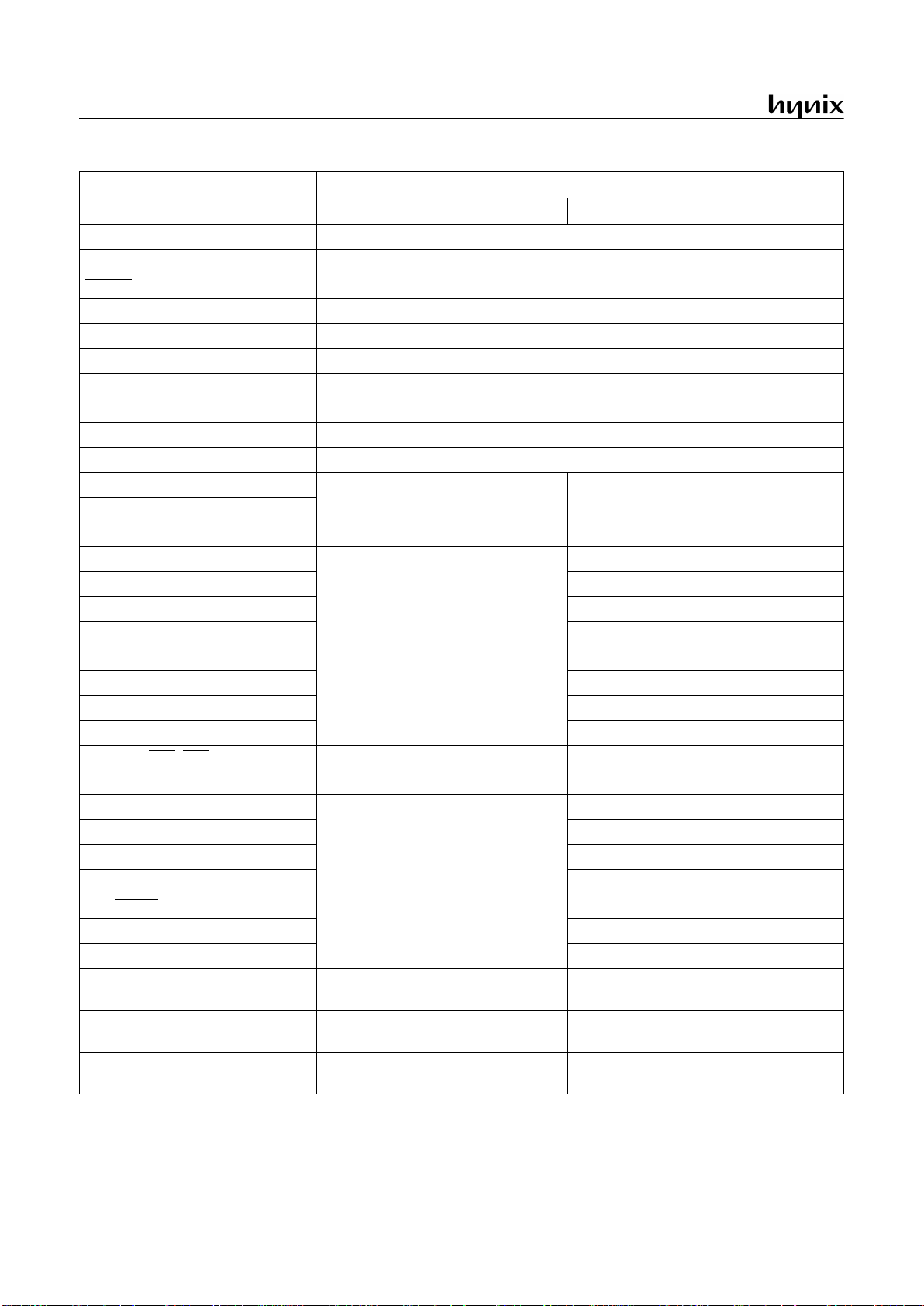
Port pin Alternate function
R00
R01
R02
R03
R04
R05
R06
R07
INT0 (External interrupt 0)
INT1 (External interrupt 1)
INT2 (External interrupt 2)
EC0 (Event counter input 0)
EC2 (Event counter input 2)
SCK (Serial clock)
SO (Serial data output)
SI (Serial data input)
Port pin Alternate function
R00
R01
KS0
(Key scan 0)
KS1
(Key scan 1)
Port pin Alternate function
R20
R21
R22
R23
R24
R25
R26
R27
AN0 (Analog Input 0)
AN1 (Analog Input 1)
AN2 (Analog Input 2)
AN3 (Analog Input 3)
AN4 (Analog Input 4)
AN5 (Analog Input 5)
AN6 (Analog Input 6)
AN7 (Analog Input 7)
Port pin Alternate function
R30
R31
R32
R33
R34
R35
R36
BUZ (Buzzer driving output)
PWM0 / T1O (PWM 0 output
/ Timer 1 output)
PWM1 /T3O (PWM 1 output
/ Timer 3 output)
WDTO
(Watchdog timer output)
SX
OUT
(Sub clock output)
SX
IN
(Sub clock input)

GMS81C7008/7016
APR., 2001 Ver 2.01 7
puts.
SEG8~SEG15
: These pins generate LCD segment signal output.
Every LCD segment pins are sh ared wit h norm al R5 in put/o utput
port. R5 is an 8-bit CMOS bidirectional I/O port. R5 pins 1 or 0
written to the Port Direction R egister can be used as outputs or in puts.
SEG16~SEG23
: These pins generate LCD segment signal output.
Every LCD segment pins are shared with normal R6 input/output
port. R6 is an 8-bit CMOS bidirectional I/O port. R6 pins 1 or 0
written to the Port Direction Re gister can be use d as outputs or in puts.
LCD pin function Port pin
SEG0 (LCD segment 0 signal output)
SEG1 (LCD segment 1 signal output)
SEG2 (LCD segment 2 signal output)
SEG3 (LCD segment 3 signal output)
SEG4 (LCD segment 4 signal output)
SEG5 (LCD segment 5 signal output)
SEG6 (LCD segment 6 signal output)
SEG7 (LCD segment 7 signal output)
R40
R41
R42
R43
R44
R45
R46
R47
LCD pin function Port pin
SEG8 (LCD segment 8 signal output)
SEG9 (LCD segment 9 signal output)
SEG10 (LCD segment 10 signal output)
SEG11 (LCD segment 11 signal output)
SEG12 (LCD segment 12 signal output)
SEG13 (LCD segment 13 signal output)
SEG14 (LCD segment 14 signal output)
SEG15 (LCD segment 15 signal output)
R50
R51
R52
R53
R54
R55
R56
R57
LCD pin function Port pin
SEG16 (LCD segment 16 signal output)
SEG17 (LCD segment 17 signal output)
SEG18 (LCD segment 18 signal output)
SEG19 (LCD segment 19 signal output)
SEG20 (LCD segment 20 signal output)
SEG21 (LCD segment 21 signal output)
SEG22 (LCD segment 22 signal output)
SEG23 (LCD segment 23 signal output)
R60
R61
R62
R63
R64
R65
R66
R67
GMS81C7008/7016
8 APR., 2001 Ver 2.01
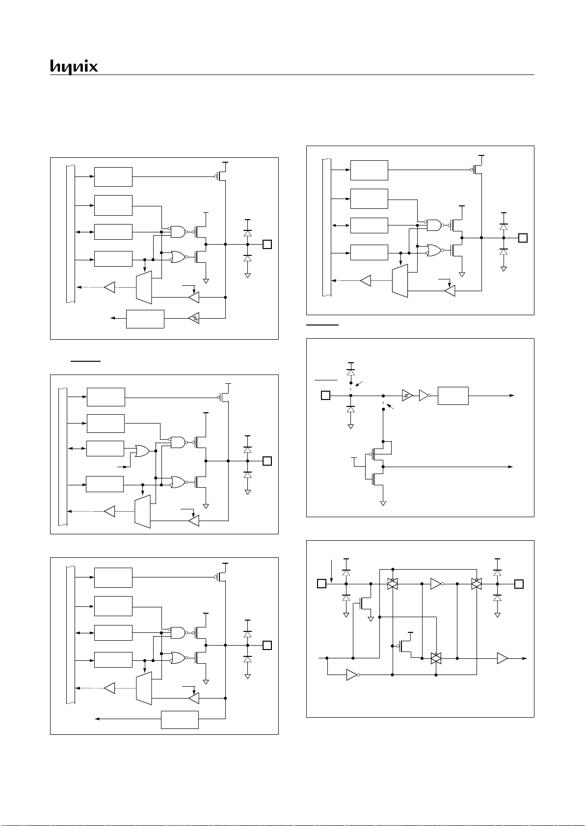
PIN NAME
(Alternate)
In/Out
(Alternate)
Function
Basic Alternate
V
DD
- Supply voltage
V
SS
- Circuit ground
RESET
I Reset signal input
AV
DD
- Supply voltage input pin for ADC
AV
SS
- Ground level input pin for ADC
X
IN
I Oscillation input
X
OUT
O Oscillation output
BIAS I LCD bias voltage input
VCL0~VCL2 I LCD driver power supply
COM0 O LCD common signal output
COM1(SEG26) O(O)
LCD common signal output LCD segment signal outputCOM2(SEG25) O(O)
COM3(SEG24) O(O)
R00 (INT0) I/O (I)
8-bit general I/O ports
External interrupt 0 input
R01 (INT1) I/O (I) External interrupt 1 input
R02 (INT2) I/O (I) External interrupt 2 input
R03 (EC0) I/O (I) Timer/Counter 0 external input
R04 (EC2) I/O (I) Timer/Counter 1 external input
R05 (SCK) I/O (I/O) Serial clock I/O
R06 (SO) I/O (O) Serial data output
R07 (SI) I/O (I) Serial data input
R10, R11(KS0
, KS1) I/O (I) 2-bit general I/O ports Key scan input
R20~R27(AN0~AN7) I/O(I) 8-bit general I/O ports Analog voltage input
R30(BUZ) I/O(O)
7-bit general I/O ports
Buzzer driving output
R31(PWM0 / T1O) I/O(O) PWM 0 output / Timer 1 output
R32(PWM1 / T3O) I/O(O) PWM 1 output / Timer 2 output
R33 I/O R34(WDTO
) I/O(O) Watchdog timer output
R35(SX
OUT
) I/O(O) Sub clock output
R36(SX
IN
) I/O(I) Sub clock input
SEG0 ~ SEG7
(R40~R47)
O (I/O) LCD segment signal output 8-bit general I/O ports
SEG8 ~ SEG15
(R50~R57)
O (I/O) LCD segment signal output 8-bit general I/O ports
SEG16 ~ SEG23
(R60~R67)
O (I/O) LCD segment signal output 8-bit general I/O ports
Table 5-1 Port Function Description
GMS81C7008/7016
APR., 2001 Ver 2.01 9
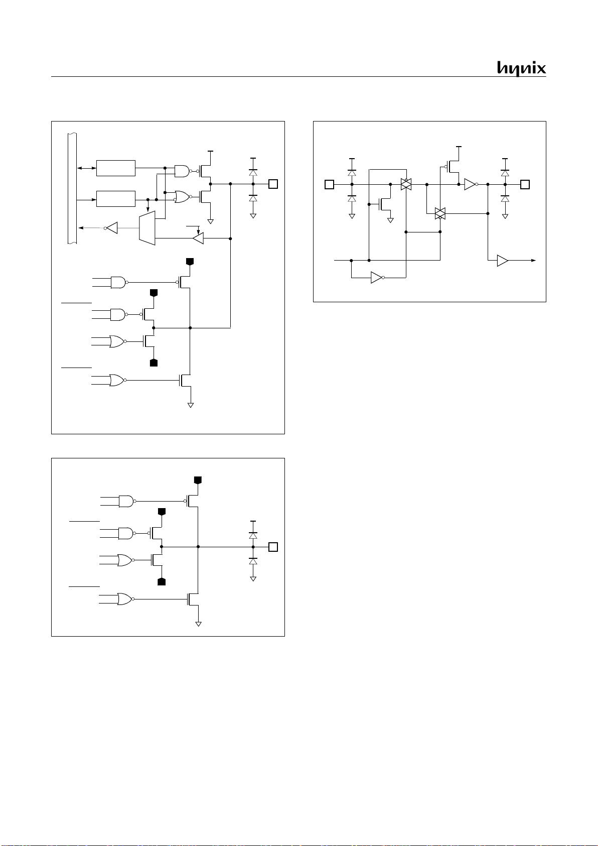
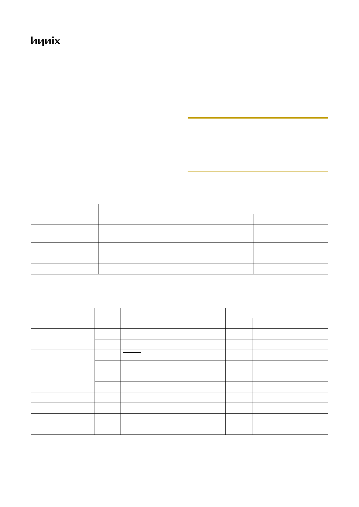
6. PORT STRUCTURES
R00/INT0, R01/INT1, R02/INT2, R03/EC0,
R04/EC2, R05/SCK, R07/S
R30/BUZ, R31/PWM0/T1O, R32/PWM1/T3O,
R34/WDTO
, R06
R20/AN0~R27/AN7
R10~R11, R33, R35, R36
RESET
SXIN, SXOUT
Pin
Data Reg.
Dir. Reg.
Noise
Canceller
INT0 ~ INT2
Pull up
Reg.
MUX
RD
V
DD
V
SS
Pull-up Tr.
EC0,EC2
Open Drain
Reg.
Data Bus
SI,SCK
Tr.: Transistor
Reg.: Register
Pin
Data Reg.
Dir. Reg.
Pull up
Reg.
MUX
V
DD
V
SS
Pull-up Tr.
Open Drain
Reg.
BUZ,SO,WDTO
Data Bus
PWM0,PWM1
RD
Pin
Data Reg.
Dir. Reg.
Analog
Switch
AN0 ~ AN7
Pull up
Reg.
MUX
RD
V
DD
V
SS
Pull-up Tr.
Open Drain
Reg.
Data Bus
Pin
Data Reg.
Dir. Reg.
Pull up
Reg.
MUX
RD
V
DD
V
SS
Pull-up Tr.
Open Drain
Reg.
Data Bus
RESET
V
SS
Noise
Canceller
Internal RESET
V
SS
V
DD
High Voltage On(OTP)
V
DD
OTP MCU :disconnected
Mask MCU :c onnected
OTP MCU :connected
Mask MCU :disconnected
SXOUT
V
SS
Internal
SXIN
Sub clock OFF
(R35)
(R36)
V
DD
System Clock
LCR.7=0
GMS81C7008/7016
10 APR., 2001 Ver 2.01
R40~R47, R50~R57, R60~R67 / SEG0~SEG23
COM0~COM3 / SEG24~SEG26
XIN, XOUT
Pin
Data Reg.
Dir. Reg.
MUX
RD
V
DD
V
SS
Data Bus
VCL2
VCL1
V
SS
VCL0
LCD Data
VCL2 Enable
LCD Data
VCL1 Enable
LCD Data
VCL0 Enable
LCD Data
GND Enable
Pin
VCL2
VCL1
V
SS
VCL0
LCD Data
VCL2 Enable
LCD Data
VCL1 Enable
LCD Data
VCL0 Enable
LCD Data
GND Enable
XOUT
V
DD
V
SS
Main Clock
XIN
STOP & Main
Clock OFF
GMS81C7008/7016
APR., 2001 Ver 2.01 11
7. ELECTRICAL CHARACTERISTICS
7.1 Absolute Maximum Ratings
Supply voltage...........................................-0.3 to +6.0 V
Storage Temperature ................................-40 to +125 °C
Voltage on any pin with respect to Ground (V
SS
)
................................ ............................... -0.3 to V
DD
+0.3
Maximum current out of V
SS
pin........................100 mA
Maximum current into V
DD
pin ............................80 mA
Maximum current sunk by (I
OL
per I/O Pin) ........ 20 mA
Maximum output current sourced by (I
OH
per I/O Pin)
...............................................................................15 mA
Maximum current (ΣI
OL
)....................................100 mA
Maximum current (ΣI
OH
)......................................60 mA
Note: Stresses above those listed under “Absolute Maximum Ratings” may cause per manent damage to the d evice. This is a stress ra ting only and functional ope r ati on of
the device at any oth er c ond iti ons ab ov e tho se ind ic ated in
the oper ati o na l se c ti ons of this s pe c if i ca t io n i s not i mp l ie d .
Exposure to absolute maximum rating conditions for extended periods may affect device reliability.
7.2 Recommended Operating Conditions
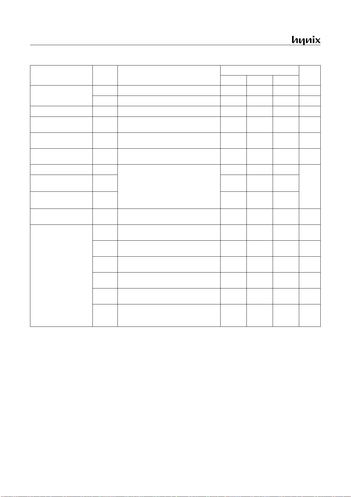
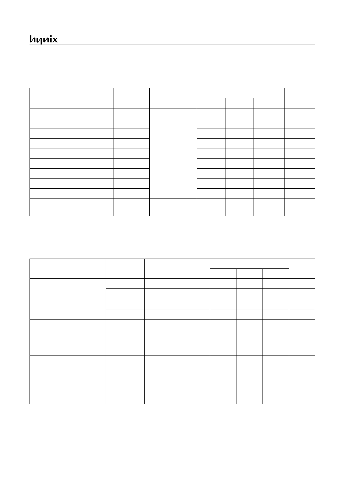
7.3 DC Electrical Characteristics
(TA=-20~85°C, VDD=2.7~5.5V)
,
Parameter Symbol Condition
Specifications
Unit
Min. Max.
Supply Voltage
V
DD
f
XIN
=4.19MHz
f
SXIN
=32.768kHz
2.7 5.5 V
Operating Frequency
f
XIN
VDD=2.7~5.5V
14.5MHz
Sub Operating Frequency
f
SXIN
VDD=2.7~5.5V
30 35 kHz
Operating Temperature
T
OPR
-20 +85
°
C
Parameter Symbol Condition
Specifications
Unit
Min. Typ. Max.
Input High Voltage
V
IH1
RESET, R0 (except R06)
0.8 V
DD
-
V
DD
V
V
IH2
Other pins
0.7 V
DD
-
V
DD
V
Input Low Voltage
V
IL1
RESET, R0 (except R06) 0 -
0.2 V
DD
V
V
IL2
Other pins 0 -
0.3 V
DD
V
Output High Voltage
V
OH1
R0,R1,R2,R3 I
OH1
=-0.5mA
V
DD
-0.1
--V
V
OH2
SEG, COM I
OH2
=-30µA--0.4V
Output Low Voltage
V
OL1
R0,R1,R2,R3 I
OL1
=0.4mA - - 0.2 V
V
OL2
SEG, COM I
OL2
=30µA
V
DD
-0.2
--V
Input High
Leakage Current
I
IH1
VIN=V
DD
, All input pins except XIN, SX
IN
--1µA
I
IH2
VIN=V
DD, XIN
, SX
IN
--20µA
GMS81C7008/7016
12 APR., 2001 Ver 2.01
Input Low
Leakage Current
I
IL1
VIN=0, All input pins except XIN, SX
IN
---1µA
I
IL2
VIN=0, XIN, SX
IN
- - -20
µ
A
Pull-up Resistor
1
R
PORT
VIN=0V, VDD=5.5V, R0, R1, R2 60 160 350 k
Ω
LCD Voltage Dividing
Resistor
R
LCD
VDD=5.5V 456585k
Ω
Voltage Drop
|V
DD
-COMn| , n=0~3
V
DC
VDD=2.7 ~ 5.5V
-15µA per common pin
--120mV
Voltage Drop
|V
DD
-SEGn| , n=0~26
V
DS
VDD=2.7 ~ 5.5V
-15µA per segment pin
--120mV
V
CL2
Output Voltage
V
CL2
VDD=2.7 ~ 5.5V, 1/3 bias
BIAS pin and VCL2 pin are shorted
V
DD
-0.3 V
DD
VDD+0.3
V
V
CL1
Output Voltage
V
CL1
0.66V
DD
-0.2
0.66V
DD
0.66V
DD
+0.3
V
CL0
Output Voltage
V
CL0
0.33V
DD
-0.3
0.33V
DD
0.33V
DD
+0.3
RC Oscillation Frequency
f
RC
R=60kΩ, VDD= 5V 123MHz
Supply Current
1
( ) means at 3V operation
I
DD1
Main clock operation mode
2
VDD=5.5V±10%, XIN=4MHz, S
XIN
=32kHz
-
2.9
(1.3)
7.0
(3.0)
mA
I
DD2
Sleep mode (Main active) 3
V
DD
=5.5V±10%, XIN=4MHz, S
XIN
=32kHz
-
0.4
(0.1)
1.7
(1.0)
mA
I
DD3
Stop mode
2
VDD=5V±10%, XIN= 0Hz, S
XIN
=
32kHz
2.0
(1.0)
12
(5)
µ
A
I
DD4
Sub clock operation mode
4
VDD=5.5V±10%, XIN=0Hz, S
XIN
=32kHz
-
350
(70)
500
(200)
µ
A
I
DD5
Sleep mode (Sub active)
5
VDD=3V±10%, XIN= 0Hz, S
XIN
=
32kHz
-
10
(3)
50
(20)
µ
A
I
DD6
Stop mode
4
VDD=5V±10%, XIN= 0Hz, S
XIN
=
0Hz
S
XIN
, SXOUT are used as R35, R36.
-
1.0
(0.5)
12
(5)
µ
A
1. Supply current in the following circuits are not included; on-chip pull-up resistors, internal LCD voltage dividing resistors, comparator voltage divide resistor, LVD circuit and output port drive currents.
2. This mode set System Clock Mode Register(SCMR) to xxxx0000
B
that is f
XIN
/2
3. This mode set SCMR to xxxx0000
B
(f
XIN
/2) and set SMR to “1”.
4. Main-frequency clock stops and sub-frequency clock in not used and set SCMR to xxxx0011
B
.
5. Main-frequency clock stops and sub-frequency clock in not used, set SCMR to xxxx0011
B
and set SMR to “1”.
Parameter Symbol Condition
Specifications
Unit
Min. Typ. Max.
GMS81C7008/7016
APR., 2001 Ver 2.01 13
7.4 A/D Converter Characteristics
(TA=25°C, VSS=0V, VDD=5.0V, AVDD=5.0V @f
XIN
=4MHz)
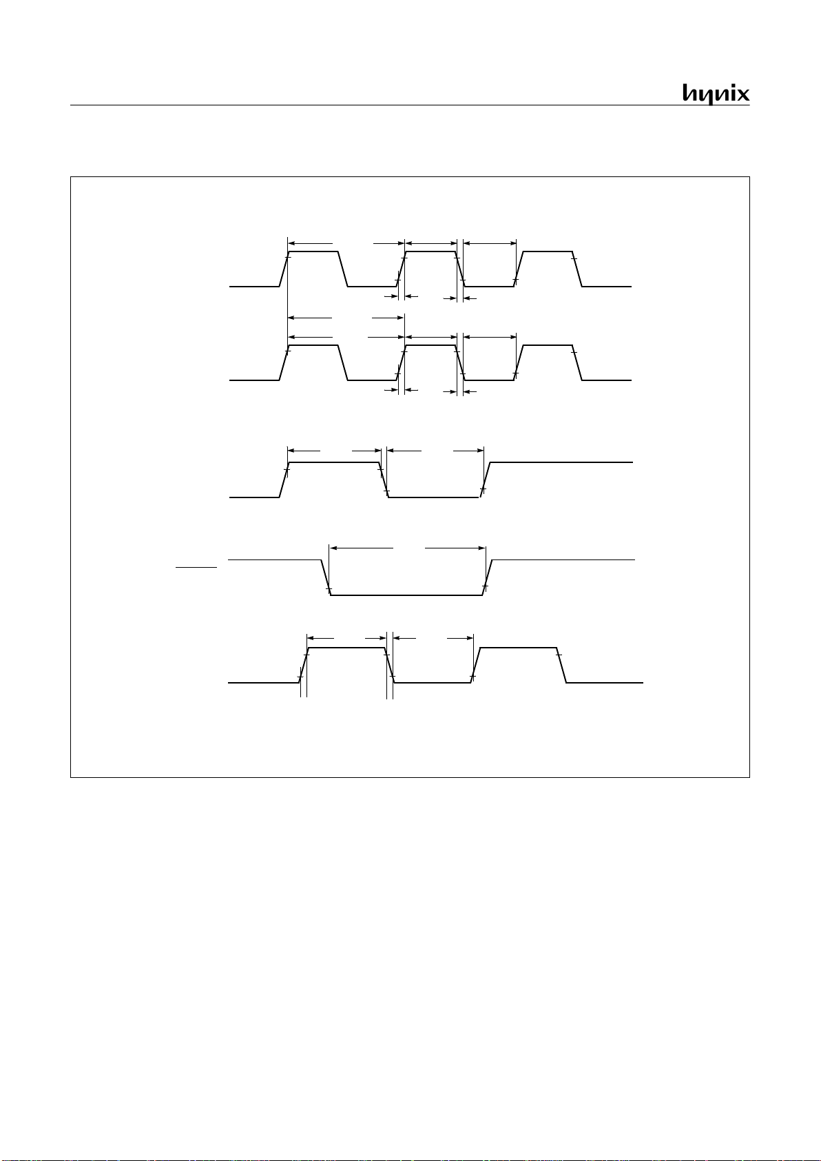
7.5 AC Characteristics
(TA=-20~+85°C, VDD=5V±10%, VSS=0V)
Parameter Symbol Test Condition
Specifications
Unit
Min.
Typ.
1
1. Data in “Typ” column is at 25°C unless otherwise stated. These parameters are for design guidance only and are not tested.
Max.
Analog Input Voltage Range
V
AIN
VDD=AVDD=5.0V
V
SS
-0.3
-
AVDD+0.3
V
Non-linearity Error
N
NLE
-
±
1.0 ±1.5 LSB
Differential Non-linearity Error
N
DNLE
-
±
1.0 ±1.5 LSB
Zero Offset Error
N
ZOE
-
±
0.5 ±1.5 LSB
Full Scale Error
N
FSE
-
±
0.25 ±0.5 LSB
Gain Error
N
GE
-
±
1.0 ±1.5 LSB
Overall Accuracy
N
ACC
-
±
1.0 ±1.5 LSB
AV
DD
Input Current
I
REF
- - 200
µ
A
Conversion Time
T
CONV
--20µs
Analog Power Supply Input Range
AV
DD
VDD=5.0V
V
DD
=3.0V
3.0
2.7
-
V
DD
V
Parameter Symbol Pins
Specifications
Unit
Min. Typ. Max.
Operating Frequency
f
MAIN
X
IN
0.455 - 4.2 MHz
f
SUB
SX
IN
30 32.768 35 kHz
External Clock Pulse W idth
t
MCPW
X
IN
80 - - nS
t
SCPW
SX
IN
14.7 - -
µ
S
External Clock Transition Time
t
MRCP,tMFCP
X
IN
- - 20 nS
t
SRCP,tSFCP
SX
IN
--3µS
Main oscillation Stabilizing
Time
t
MST
XIN, X
OUT
at 4MHz
--20mS
Sub oscillation Stabilizing Time
t
SST
SXIN, SX
OUT
-0.51 S
Interrupt Pulse Width
t
IW
INT0, INT1, INT2 2 - -
t
SYS
1
RESET Input Width
t
RST
RESET 8--t
SYS
1
Event Counter Input Pulse
Width
t
ECW
EC0, EC2 2 - -
t
SYS
1
1. t
SYS
is one of 2/f
MAIN
or 8/f
MAIN
or 16/f
MAIN
or 64/f
MAIN
in the main clock operation mode,
t
SYS
is one of 2/f
SUB
or 8/f
SUB
or 16/f
SUB
or 64/f
SUB
in the sub clock operation mode.
GMS81C7008/7016
14 APR., 2001 Ver 2.01
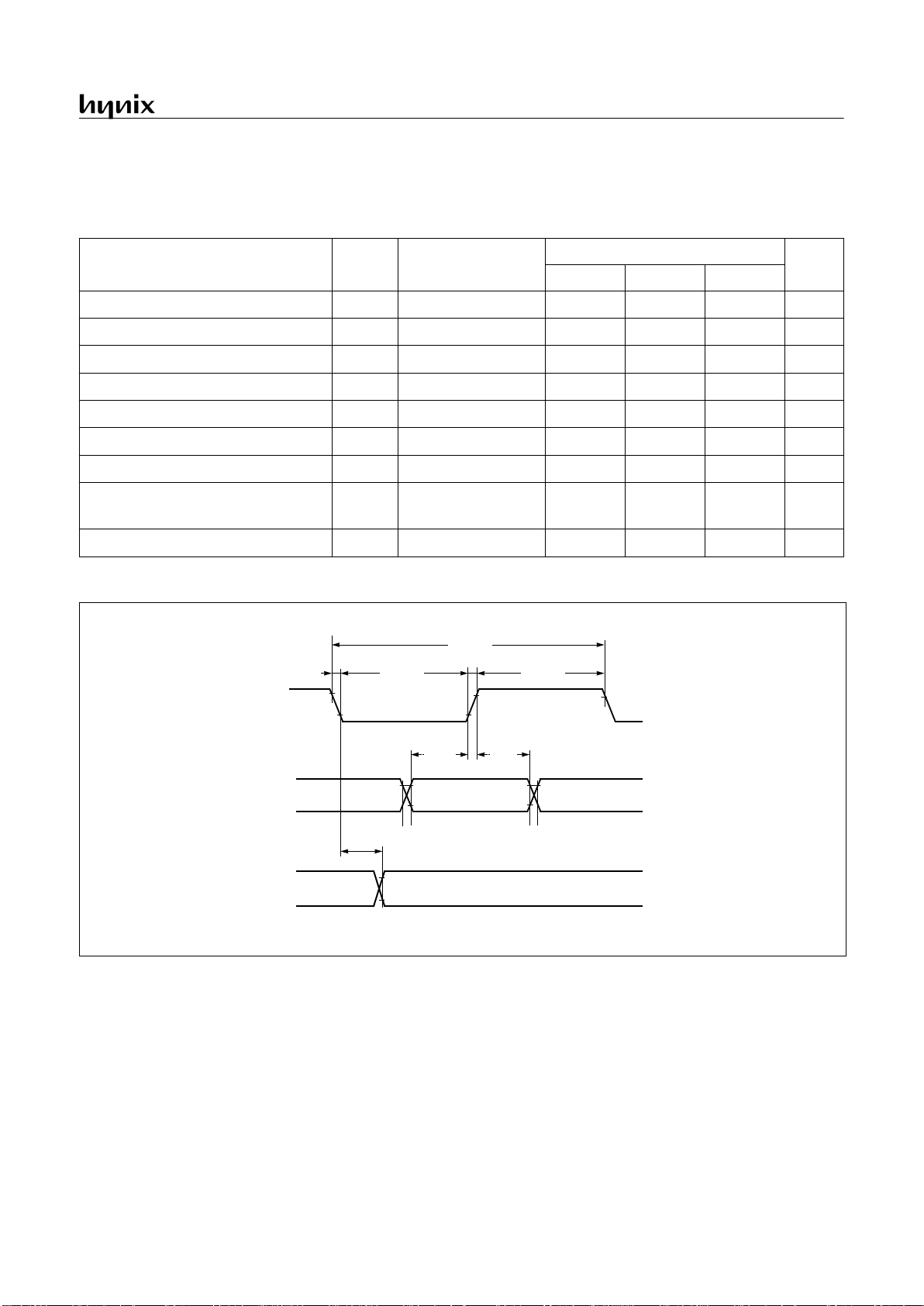
Figure 7-1 Timing Chart
t
MRCP
t
MFCP
X
IN
INT0, INT1
INT2
0.5V
V
DD
-0.5V
0.2V
DD
0.8V
DD
0.2V
DD
RESET
0.2V
DD
0.8V
DD
EC0, EC2
t
IW
t
IW
t
RST
t
ECW
t
ECW
1/f
MAIN
t
MCPW
t
MCPW
t
SRCP
t
SFCP
SX
IN
0.5V
V
DD
-0.5V
1/f
SUB
t
SCPW
t
SCPW
t
SYS
GMS81C7008/7016
APR., 2001 Ver 2.01 15
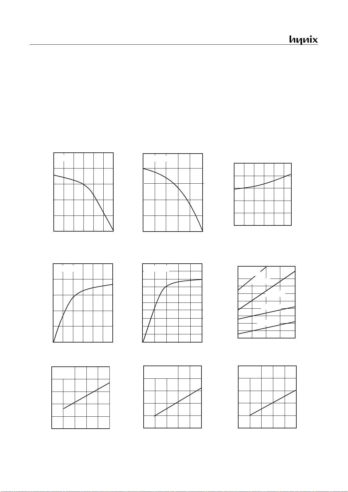
7.6 Serial Interface Timing Characteristics
(TA=-20~+85°C, VDD=2.7~5.5V, VSS=0V, f
XIN
=4MHz)
Figure 7-2 Serial I/O Timing Chart
Parameter Symbol Pins
Specifications
Unit
Min. Typ. Max.
Serial Input Clock Pulse
t
SCYC
SCK
2t
SYS
+200
-8ns
Serial Input Clock Pulse Width
t
SCKW
SCK
t
SYS
+70
-8ns
SIN Input Setup Time (External SCK)
t
SUS
SIN 100 - - ns
SIN Input Setup Time (Internal SCK)
t
SUS
SIN 200 - - ns
SIN Input Hold Time
t
HS
SIN
t
SYS
+70
--ns
Serial Output Clock Cycle Time
t
SCYC
SCK
4t
SYS
-
16t
SYS
ns
Serial Output Clock Pulse Width
t
SCKW
SCK
t
SYS
-30
--ns
Serial Output Clock Pulse Transition
Time
t
FSCK
t
RSCK
SCK - - 30 ns
Serial Output Delay Time
s
OUT
SO - - 100 ns
SCLK
SIN
0.2V
DD
SOUT
0.2V
DD
0.8V
DD
t
SCYC
t
SCKW
t
SCKW
t
RSCK
t
FSCK
0.8V
DD
t
SUS
t
HS
t
DS
0.2V
DD
0.8V
DD
GMS81C7008/7016
16 APR., 2001 Ver 2.01
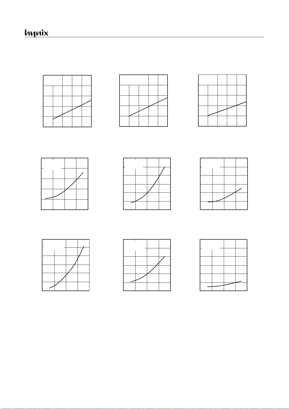
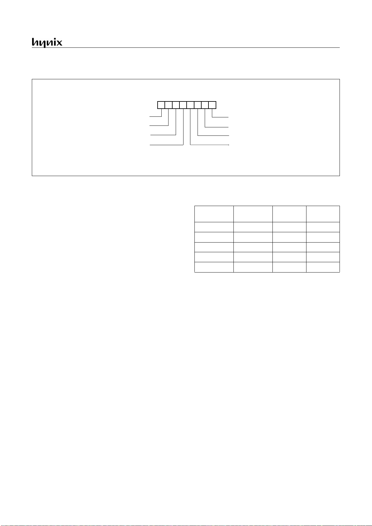
7.7 Typical Characteristics
This graphs and tables provided in this section are for design guidance only and are not tested or guaranteed.
In some graphs or tables the data presented are outside specified operating range (e.g. outside specified
VDD range). This is for information only and devices
are guaranteed to operate properly only within the
specified range.
The data presented in this s ection is a statistical s ummary
of data collected on units from different lots over a period
of time. “Typical” represents the mean of the distribution
while “max” or “min” represents (mean + 3σ) and (mean
−
3σ) respectively where σ is standard deviation
I
OL
−−−−
V
OL
, VDD=5.5V
40
30
20
10
0
(mA)
I
OL
V
OL
(V)
I
OL
−−−−
V
OL
, VDD=3.0V
(mA)
I
OL
0.5 1.0 1.5 2.0 2.5
V
OL
(V)
I
OH
−−−−
V
OH
, VDD=5.0V
-20
-15
-10
-5
0
(mA)
I
OH
12345
V
OH
(V)
I
OH
−−−−
V
OH
, VDD=3.0V
-8
-6
-4
-2
0
(mA)
I
OH
0.5 1.0 1.5 2.0 2.5
V
OH
(V)
Ta=25°C
R0,R1,R2,R3 pin
200
100
0
(kΩ)
-20
04080
Ta
(°C)
R
12345
f
XIN
=4MHz
V
DD
−−−−
V
IH1
4
3
2
1
0
(V)
V
IH1
23
45
6
V
DD
(V)
V
DD
−−−−
V
IH2
4
3
2
1
0
(V)
V
IH2
23
45
6
V
DD
(V)
Ta=25°C
f
XIN
=4MHz
Ta=25°C
1
R0 (except R06)
R1~R6 pin
20
15
10
5
(include R06)
f
XIN
=4MHz
V
DD
−−−−
V
IH3
4
3
2
1
0
(V)
V
IH1
23
45
6
V
DD
(V)
Ta=25°C
1
XIN, SX
IN
R = 6.2k
Ω
4
3
2
1
0
(MHz)
f
XIN
2345
6
V
DD
(V)
Ta=25°C
R = 20k
Ω
R = 180k
Ω
R = 60k
Ω
f
XIN
−−−−
V
DD
Ta=25°C
Ta=25°CTa=25°C
R
PU
−−−−
T
a
, VDD=5.0V
GMS81C7008/7016
APR., 2001 Ver 2.01 17
I
STOP
((((
I
DD6
)
−−−−
V
DD
STOP Mode
I
DD1
−−−−
V
DD
4
3
2
1
0
(mA)
I
DD
6
V
DD
(V)
Normal Operation (Main opr.)
I
DD4
−−−−
V
DD
400
300
200
100
0
(µA)
I
DD
23
45
6
V
DD
(V)
Normal Mode (Sub opr.)
I
SLEEP(IDD5
)
−−−−
V
DD
SLEEP Mode (Sub opr.)
I
SLEEP(IDD2
)
−−−−
V
DD
f
XIN
=4MHz
V
DD
−−−−
V
IL1
4
3
2
1
0
(V)
V
IH1
23
45
6
V
DD
(V)
V
DD
−−−−
V
IL2
4
3
2
1
0
(V)
V
IH2
23
45
6
V
DD
(V)
Ta=25°C
f
XIN
=4MHz
Ta=25°C
1
R0 (except R06)
R1~R6 pin
(include R06)
f
XIN
=4MHz
V
DD
−−−−
V
IL3
4
3
2
1
0
(V)
V
IH1
23
45
6
V
DD
(V)
Ta=25°C
1
XIN, SX
IN
23
45
SLEEP Mode (Main opr.)
f
SXIN
=32kHz
Ta=25°C
400
300
200
100
0
(µA)
I
DD
23
45
6
V
DD
(V)
12
9
6
3
0
(µA)
I
DD
23
45
6
V
DD
(V)
f
SXIN
=32kHz
Ta=25°C
I
STOP(IDD3
)
−−−−
V
DD
STOP Mode
4
3
2
1
0
(µA)
I
DD
23
45
6
V
DD
(V)
f
XIN
=0Hz
Ta=25°C
f
XIN
=4MHz
Ta=25°C
f
XIN
=4MHz
Ta=25°C
4
3
2
1
0
(µA)
I
DD
23
45
6
V
DD
(V)
f
SXIN
=0Hz
Ta=25°C

GMS81C7008/7016
18 APR., 2001 Ver 2.01
8. MEMORY ORGANIZATION
The GMS81C7008/16 has separate address spaces for Program
memory and Data Memory. Program memory can only be read,
not written to. It can be u p to 8 K/16 K b yt es of Pro gram me m ory.
Data memory can be read and written to up to 448 bytes including
the stack area and the LCD display RAM area.
8.1 Registers
This device has six registers that are the Program Counter (PC),
a Accumulator (A), two index registers (X, Y), the Stack Pointer
(SP), and the Program Status Word (PSW). The Program Counter
consists of 16-bit register.
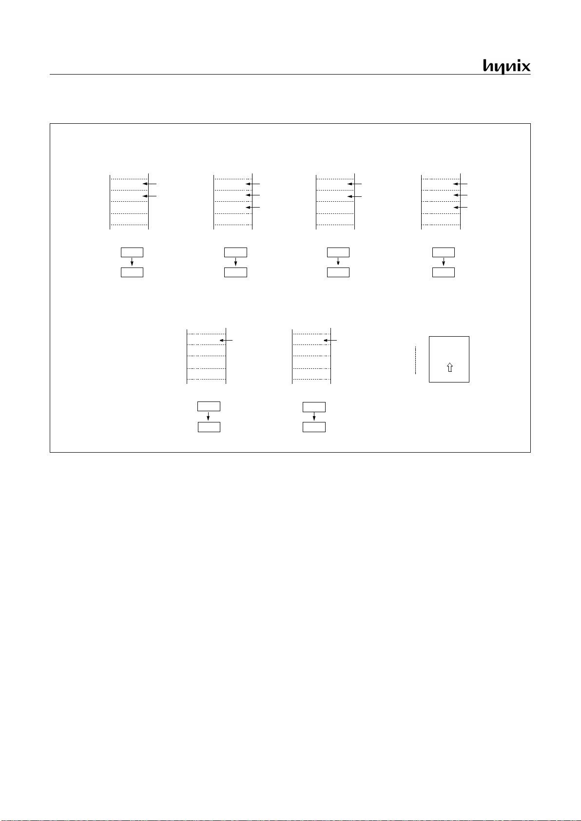
Figure 8-1 Configuration of Registers
Accumulator:
The Accumulator is the 8-bit general purpose register, used for data operat ion such as transfe r, tempor ary sav ing,
and conditional judgement, etc.
The Accumulator can be used as a 1 6-bit register with Y Register
as shown below.
Figure 8-2 Configuration of YA 16-bit Register
X, Y Registers
: In the addressing mode which uses these index
registers, the register contents are adde d to the specified address,
which becomes the actual address. These modes are extremely effective for referencing subroutine tables and memory tables. The
index registers also hav e incremen t, decremen t, compari son and
data transfer functions, and they can be used as simple accumulators.
Stack Pointer
: The Stack Pointer is an 8-bit register used for occurrence interrupts and calling out subroutines. Stack Pointer
identifies the location in the stack to be access (save or restore).
Generally, SP is automatically updated when a subroutine call is
executed or an interrupt is accepted. However, if it is used in ex-
cess of the stack area permitted by the data memory allocating
configuration, the user-processed data may be lost.
The stack can be located at any po sit ion wit hin 01 1B
H
to 01FF
H
of the internal data memory. The SP is not initialized by hardware, requiring to write the initial value (the location with which
the use of the stack starts) by using the initializ ation routin e. Normally, the initial value of “FF
H
” is used.
Note: The Stack Pointer must be initialized by software because its value is undefined after RESET.
Example: To initialize the SP
LDX #0FFH
TXSP ; SP ← FFH
Program Counter
: The Program Counter is a 16-bit wide which
consists of t wo 8-b it regi sters, P CH an d PC L. Thi s co un ter ind icates the address of the next in struction to be execut ed. In reset
state, the program counter has reset routine address (PC
H
:0FFH,
PC
L
:0FEH).
Program Status Word
: The Program Status Word (PSW) contains several bits that reflect the current state of the CPU. The
PSW is described in Figure 8-3. It contains the Negative flag, the
Overflow flag, the Break flag the Half Carry (for BCD operation), the Interrupt enable flag, the Zero flag, and the Carry flag.
[Carry flag C]
This flag stores any carry or not borrow from the ALU of CPU
after an arithmetic operation and is also changed by the Shift Instruction or Rotate Instruction.
[Zero flag Z]
This flag is set when the result of an arithmetic operation or data
transfer is “0” and is cleared by any other result.
ACCUMULATOR
X REGISTER
Y REGISTER
STACK POINTER
PROGRAM COUNTER
PROGRAM STATUS
WORD
X
A
SP
Y
PCL
PSW
PCH
Two 8-bit Registers can be used as a “YA” 16-bit Register
Y
A
Y A
SP
01
H
Stack Area (100H ~ 1FFH)
Bit 15 Bit 087
Hardware fixed
00H~FF
H
LCD display RAM area is located in 100H~11AH,
SP (Stack Pointer) could be in 00
H
~FFH.
User must have concerning that Stack data does not
cross over LCD RAM area.
GMS81C7008/7016
APR., 2001 Ver 2.01 19
Figure 8-3 PSW (Program Status Word) Register
[Interrupt disable flag I]
This flag enables/disables all interrupts except interrupt caused
by Reset or software BRK instruction. All interrupts are disabled
when cleared to “0”. This flag immediately becomes “0” when an
interrupt is served. It i s set by the EI instruction and cleared by
the DI instruction.
[Half carry flag H]
After operation, this is set when there is a carry from bit 3 of ALU
or there is no borrow from bit 4 of ALU. This bit can not be set
or cleared except CLRV instruction with Overflow flag (V).
[Break flag B]
This flag is set by software BRK instruction to distinguish BRK
from TCALL instruction with the same vector address.
[Direct page flag G]
This flag assigns RAM page for direct addressing mode. In the d i-
rect addressing mode, addressing area is from zero page 00
H
to
0FF
H
when this flag is "0". If it is set to "1", addressing area is
assigned by RPR register (address 0F3
H
). It is set by SETG in-
struction and clear ed by CLRG.
When content of RPR is above 2, malfunction will be occurred.
[Overflow flag V]
This flag is set to “1” when an overflow occurs as the result of an
arithmetic operation involving signs. An overflow occurs when
the result of an addition or subtraction exceeds +127(7FH) or 128(80
H
). The CLRV instruction clears the overflow flag. There
is no set instruction. When the BIT instruction is executed, bit 6
of memory is copied to this flag.
[Negative flag N]
This flag is set to match the sign bit (bit 7) status of the result of
a data or arithmetic operation. When the BIT instruction is executed, bit 7 of memory is copied to this flag.
N
NEGATIVE FLAG
V G B H I Z C
MSB LSB
RESET VALUE: 00
H
PSW
OVERFLOW FLAG
BRK FLAG
CARRY FLAG RECEIVES
ZERO FLAG
INTERRUPT ENABLE FLAG
CARRY OUT
HALF CARRY FLAG RECEIVES
CARRY OUT FROM BIT 1 OF
ADDITION OPERLANDS
SELECT DIRECT PAGE
when G=1, page is selected to “page 1”
RAM Page Instruction
Bit1 of
RPR
Bit0 of
RPR
0 page CLRG X X
0 page SETG 0 0
1 page SETG 0 1
Reserved SETG 1 0
Reserved SETG 1 1
GMS81C7008/7016
20 APR., 2001 Ver 2.01
Figure 8-4 Stack Operation
At execution of
a CALL/TCALL/PCALL
PCL
PCH
01FC
SP after
execution
SP before
execution
01FD
01FD
01FE
01FF
01FF
Push
down
At acceptance
of interrupt
PCL
PCH
01FC
01FC
01FD
01FE
01FF
01FF
Push
down
PSW
At execution
of RET instruction
PCL
PCH
01FC
01FF
01FD
01FE
01FF
01FD
Pop
up
At execution
of RET instruction
PCL
PCH
01FC
01FF
01FE
01FE
01FF
01FC
Pop
up
PSW
0100H
01FFH
Stack
depth
At execution
of PUSH instruction
A
01FC
01FE
01FD
01FE
01FF
01FF
Push
down
SP after
execution
SP before
execution
PUSH A (X,Y,PSW)
At execution
of POP instruction
A
01FC
01FF
01FD
01FE
01FF
01FE
Pop
up
POP A (X,Y,PSW)

GMS81C7008/7016
APR., 2001 Ver 2.01 21
8.2 Program Memory
A 16-bit program counter is capable of addressing up to 64K
bytes, but this device has 8K/16K bytes program memory space
only physically implemented. Accessing a location above FFFF
H
will cause a wrap-around to 0000H.
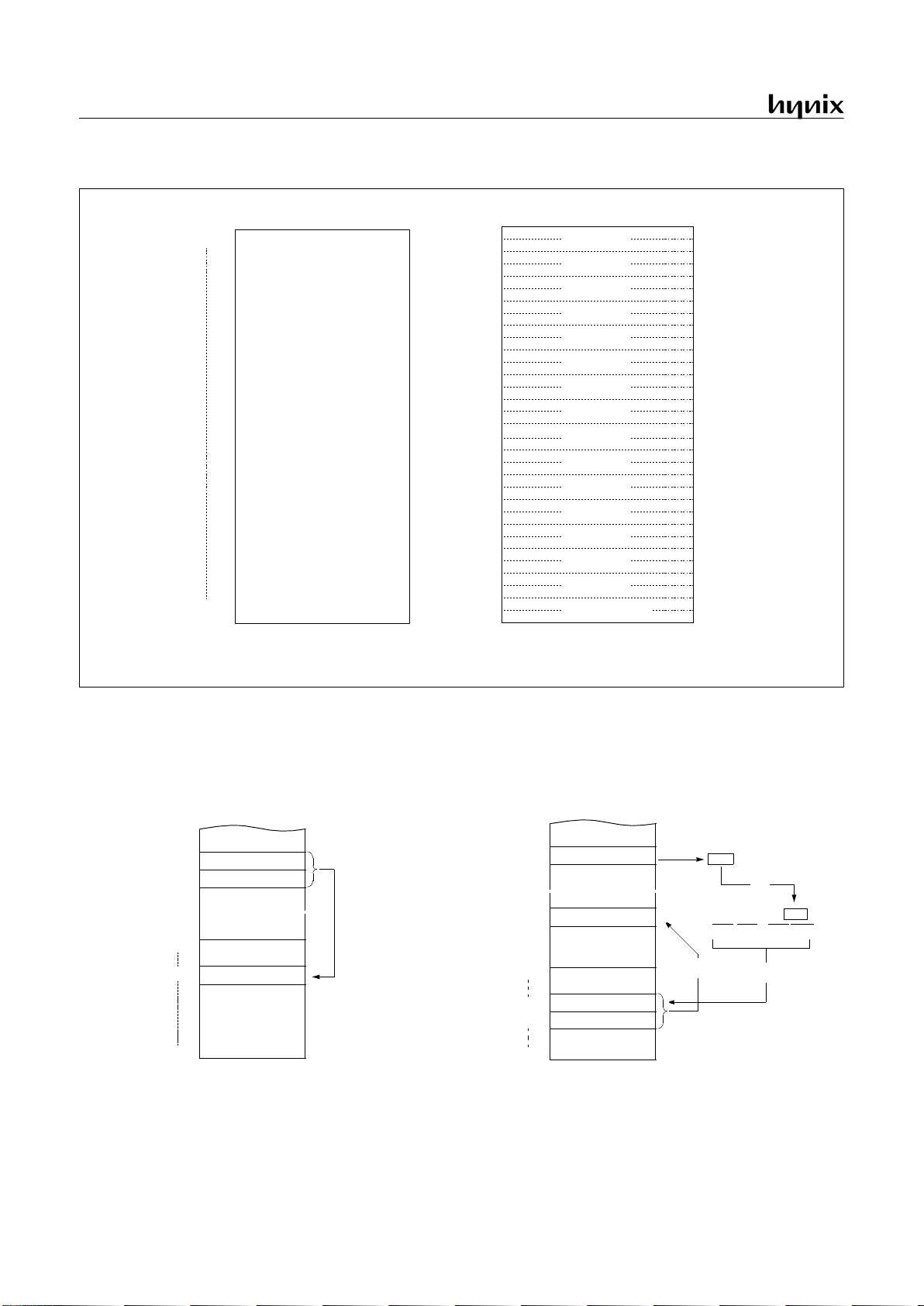
Figure 8-5, shows a map of Program Memory. After reset, the
CPU begins execution from reset vector which is stored in address FFFE
H
and FFFFH as shown in Figure 8-6.
As shown in Figure 8-5, each area is assigned a fixed location i n
Program Memory. Prog ram Me mory ar ea co ntain s the u ser p rogram.
Figure 8-5 Program Memory Map
Page Call (PCALL) area contains subroutine program to reduce
program byte lengt h by usi ng 2 bytes PCALL inst ead of 3 by tes
CALL instruction. If it is frequently called, it is more useful to
save program byte length.
Table Call (TCALL) causes the CPU to jump to each TCALL ad-
dress, where it commences the execution of the service routine.
The Table Call service area spaces 2-byte for every TCALL:
0FFC0H for TCALL15, 0FFC2H for TCALL14, etc., as shown in
Figure 8-7.
Example: Usage of TCALL
The interrupt causes the CPU to jump to specific locati on, whe re
it commences the execution of the service routine. The External
interrupt 0, for example, is assigned to location 0FFFA
H
. The in-
terrupt service locations spaces 2-byte interval: 0FFF8
H
and
0FFF9
H
for External Interrupt 1, 0FFFAH and 0FFFBH for Exter-
nal Interrupt 0, etc.
Any area from 0FF00H to 0FFFFH, if it is not going to be used,
its service location is availab le as general p urpose Program Memory.
Figure 8-6 Interrupt Vector Area
Interrupt
Vector Area
C000
H
FEFF
H
FF00
H
FFC0
H
FFDF
H
FFE0
H
FFFF
H
PCALL area
E000
H
TCALL area
GMS81C7008
8K ROM
GMS81C7016
16K ROM
0FFE0
H
E2
Address Vector Area Memory
E4
E6
E8
EA
EC
EE
F0
F2
F4
F6
F8
FA
FC
FE
Timer/Counter 3
Timer/Counter 2
Watch Timer
A/D Converter
-
External Interrupt 0
Timer/Counter 1
Basic Interval Timer
Key Scan
RESET
Watchdog Timer
Serial Peripheral Interface
“-” means reserved area.
NOTE:
External Interrupt 2
External Interrupt 1
Timer/Counter 0
-
-
GMS81C7008/7016
22 APR., 2001 Ver 2.01
Figure 8-7 PCALL and TCALL Memory Area
PCALL
→
→ →
→
rel
4F35 PCALL 35H
TCALL
→
→ →
→
n
4A TCALL 4
0FFC0
H
C1
Address Program Memory
C2
C3
C4
C5
C6
C7
C8
0FF00
H
Address
PCALL Area Memory
0FFFF
H
PCALL Area
(256 Bytes)
* means that the BRK software interrupt is using
same address with TCALL0.
NOTE:
TCALL 15
TCALL 14
TCALL 13
TCALL 12
TCALL 11
TCALL 10
TCALL 9
TCALL 8
TCALL 7
TCALL 6
TCALL 5
TCALL 4
TCALL 3
TCALL 2
TCALL 1
TCALL 0 / BRK *
C9
CA
CB
CC
CD
CE
CF
D0
D1
D2
D3
D4
D5
D6
D7
D8
D9
DA
DB
DC
DD
DE
DF
4F
~
~
~
~
NEXT
35
0FF35
H
0FF00
H
0FFFF
H
11111111 11010110
01001010
PC:
FH FH DH 6H
4A
~
~
~
~
25
0FFD6
H
0FF00
H
0FFFF
H
D1
NEXT
0FFD7
H
0D125
H
Reverse
1
2
3

GMS81C7008/7016
APR., 2001 Ver 2.01 23
Example: The usage software example of Vector address for GMS81C7016.
ORG 0FFE0H
DW TIMER3 ; Timer-3
DW TIMER2 ; Timer-2
DW WATCH_TIM ER ; Watch Timer
DW ADC ; ADC
DW SIO ; Serial Interface
DW NOT_USED ; DW NOT_USED ; DW INT2 ; Int.2
DW TIMER1 ; Timer-1
DW TIMER0 ; Timer-0
DW INT1 ; Int.1
DW INT0 ; Int.0
DW WD_TIMER ; Watchdog Timer
DW BIT_TIMER ; Basic Interval Timer
DW KEYSCAN ; Key Scan Timer
DW RESET ; Reset
ORG 0C000H ; in case of 16K ROM Start address
; ORG 0E000H ; in case of 8K ROM Start address
;*******************************************
; MAIN PROGRAM *
;*******************************************
;
RESET: LDM SCMR,#0 ;When main clock mode
DI ;Disable All Interrupts
LDM WDTR,#0 ;Disable Watch Dog Timer
LDM RPR,#1
CLRG
LDX #0
RAM_CLR: LDA #0 ;RAM Clear(!0000H ~ !00BFH)
STA {X}+
CMPX #0C0H
BNE RAM_CLR
SETG
LDX #0
RAM_CLR1:
LDA #0
STA {X}+
CMPX #1BH ;DISPLAY RAM Clear(!0100H ~ !011AH)
BNE RAM_CLR1
CLRG
;
LDX #0FFH ;Stack Pointer Initialize
TXSP
;
LDM R0, #0 ;Normal Port 0
LDM R0DD,#82H ;Normal Port Direction
LDM R0PU,#0 ;Normal Pull Up
:
:
:
LDM TDR0,#250 ;8us x 250 = 2000us
LDM TM0,#0000_1111B ;Start Timer0, 8us at 4MHz
LDM IRQH,#0
LDM IRQL,#0
LDM IENH,#0000_1110B ;Enable INT0, INT1, Timer0
LDM IENL,#0
LDM IEDS,#15H ;Select falling edge detect on INT pin
LDM PMR,#3H ;Set external interrupt pin(INT0, INT1)
EI ;Enable master interrupt
GMS81C7008/7016
24 APR., 2001 Ver 2.01
8.3 Data Memory
Figure 8-8 shows the internal Data Memory space available. Data
Memory is divided into f our g roups, a user RA M, cont rol registers, Stack, and LCD memory.
Figure 8-8 Data Memory Map
User Memory
The both GMS81C7008/16 has 448 × 8 bits for the user memory
(RAM).
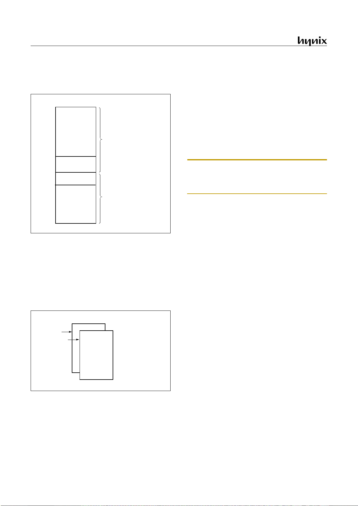
There are two page internal RAM. Page is selected by G-flag and
RAM page selection register RPR. When G-flag is cleared to “0”,
always page 0 is selected regardless of RPR value. If G-flag is set
to “1”, page will be selected ac cording to RPR value.
Figure 8-9 RAM page configuration
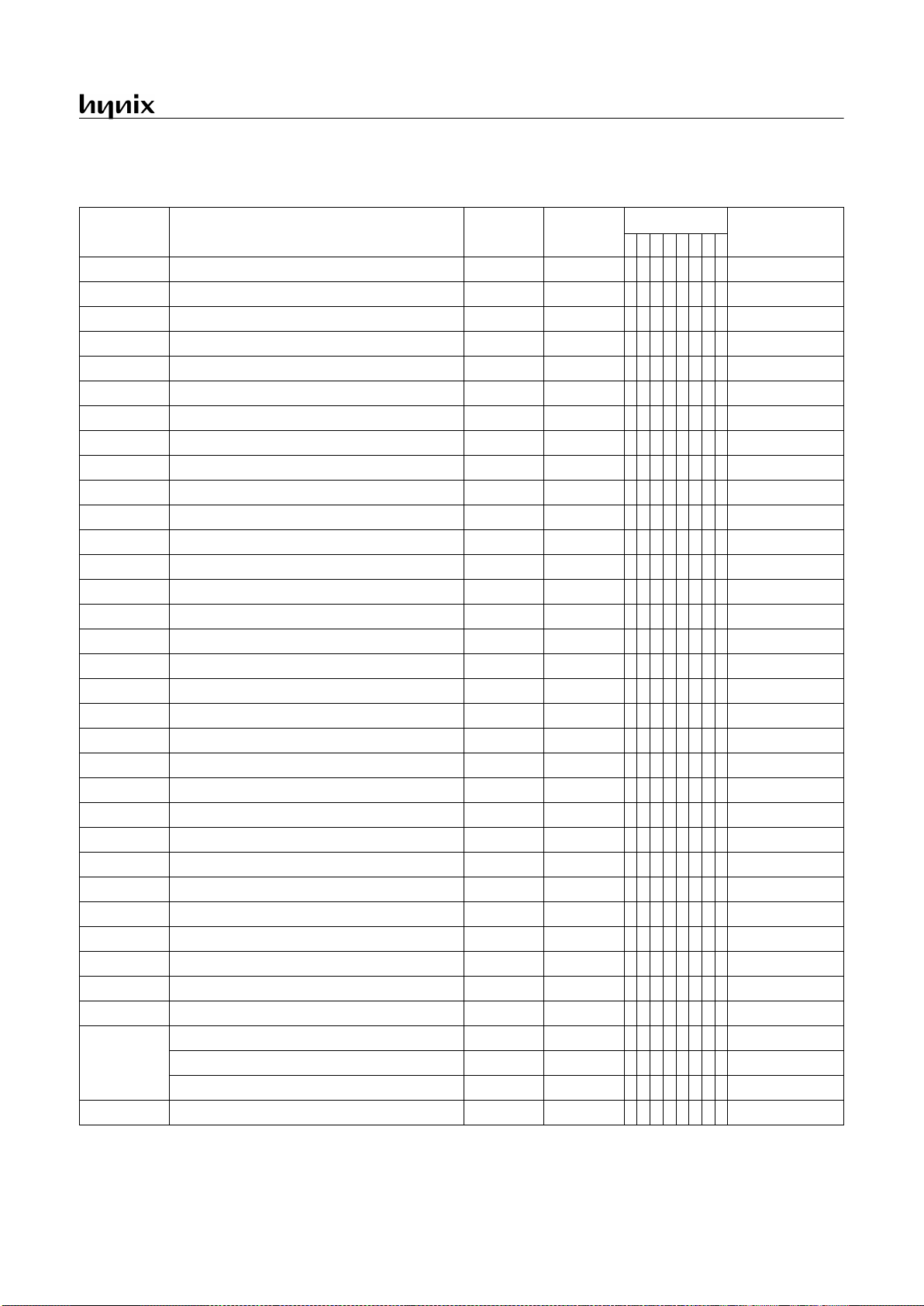
Control Registers
The control registers are used by the CPU and Peripheral function
blocks for controlling the desired operation of the device. T herefore these registers contain control and status bits for the interrupt
system, the timer/ counters, anal og to digital con verters and I/O
ports. The control registers are in address range of 0C0
H
to 0FFH.
Note that unoccupi ed addres ses may not be implem ented o n the
chip. Read accesses to these addresses will in general return random data, and write accesses will have an indeterminate effect.
More detailed informations of each register are explained in each
peripheral section.
Note: Write only registers can not be accessed by bit manipulation instruction (SET 1, CLR1 ). Do not use read-modify-write instruction. Use byte manipulation instruction, for
example “LDM”.
Example; To write at CKCTLR
LDM CKCTLR,#09H
;Divide ratio(÷16)
Stack Area
The stack p r ov i d es t h e area where the return address is sav ed before a jump is performed during the processing routine at th e execution of a subroutine call instruction or the acceptance of an
interrupt.
When returning from the processing routine, executing the subroutine return instruction [RET] restores the contents of the program counter from the stack; executing the interrupt return
instruction [RETI] restores the contents of the program counter
and flags.
The save/restore locations in the stack are determined by the
stack pointed (SP). The SP is automatically decreased after the
saving, and increased before the restoring. This means the value
of the SP indicates the stack location number for the next save.
Refer to Figure 8-4 on page 20.
User Memory
Control
Registers
or Stack Area
0000
H
00BF
H
00C0
H
00FF
H
0100
H
01FF
H
PAGE0
User Memory
PAGE1
LCD display RAM
(27 Nibbles)
011A
H
011B
H
(192 Bytes)
(229 Bytes)
Page 0
Page 0: 00~FF
H
Page 1
Page 1: 100~1FF
H
RPR=1, G=1
G=0
GMS81C7008/7016
APR., 2001 Ver 2.01 25
8.4 List of Control Registers
Address Register Name Symbol R/W
Initial Value
Page
76543210
00C0 R0 port data register R0 R/W 0 0 0 0 0 0 0 0 page 33
00C1 R1 port data register R1 R/W - - - - - - 0 0 page 33
00C2 R2 port data register R2 R/W 0 0 0 0 0 0 0 0 page 33
00C3 R3 port data register R3 R/W - 0 0 0 0 0 0 0 page 33
00C4 R4 port data register R4 R/W 0 0 0 0 0 0 0 0 page 34
00C5 R5 port data register R5 R/W 0 0 0 0 0 0 0 0 page 34
00C6 R6 port data register R6 R/W 0 0 0 0 0 0 0 0 page 35
00C8 R0 port I/O direction register R0DD W 0 0 0 0 0 0 0 0 page 35
00C9 R1 port I/O direction register R1DD W - - - - - - 0 0 page36
00CA R2 port I/O direction register R2DD W 0 0 0 0 0 0 0 0 page 36
00CB R3 port I/O direction register R3DD W - 0 0 0 0 0 0 0 page 35
00CC R4 port I/O direction register R4DD W 0 0 0 0 0 0 0 0 page 36
00CD R5 port I/O direction register R5DD W 0 0 0 0 0 0 0 0 page 36
00CE R6 port I/O direction register R6DD W 0 0 0 0 0 0 0 0 page 36
00D0 R0 port pull-up register R0PU W 0 0 0 0 0 0 0 0 page 33
00D1 R1 port pull-up register R1PU W - - - - - - 0 0 page 33
00D2 R2 port pull-up register R2PU W 0 0 0 0 0 0 0 0 page 33
00D3 R3 port pull-up register R3PU W - 0 0 0 0 0 0 0 page 33
00D4 R0 port open drain control register R0CR W 0 0 0 0 0 0 0 0 page 33
00D5 R1 port open drain control register R1CR W - - - - - - 0 0 page 33
00D6 R2 port open drain control register R2CR W 0 0 0 0 0 0 0 0 page 33
00D7 R3 port open drain control register R3CR W - 0 0 0 0 0 0 0 page 33
00D8 Ext. interrupt edge selection register IEDS R/W - - 0 0 0 0 0 0 page 69
00D9 Port mode register PMR R/W 0 0 0 0 0 0 0 0 page 62, page 69
00DA Interrupt enable lower byte register IENL R/W 0 - - 0 0 0 0 0 page 65
00DB Interrupt enable upper byte register IENH R/W - 0 0 0 0 0 0 0 page 65
00DC Interrupt request flag lower byte register IRQL R/W 0 - - 0 0 0 0 0 page 64
00DD Interrupt request flag upper byte register IRQH R/W - 0 0 0 0 0 0 0 page 64
00DE Sleep mode register SMR W - - - - - - - 0 page 81
00DF Watch dog timer register WDTR R/W - - 0 1 0 0 1 0 page 79
00E0 Timer0 mode register TM0 R/W - - 0 0 0 0 0 0 page 45
00E1
Timer0 counter register T0 R 0 0 0 0 0 0 0 0 page 45
Timer0 data register TDR0 W 1 1 1 1 1 1 1 1 page 45
Timer0 input capture register CDR0 R 0 0 0 0 0 0 0 0 page 45
00E2 Timer1 mode register TM1 R/W 00000000 page45
Table 8-1 Control Re gisters

GMS81C7008/7016
26 APR., 2001 Ver 2.01
00E3
Timer1 data register TDR1 W 1 1 1 1 1 1 1 1 page 45
PWM0 pulse period register T1PPR W 1 1 1 1 1 1 1 1 page 54
00E4
Timer1 counter register T1 R 0 0 0 0 0 0 0 0 page 45
Timer1 input capture register CDR1 R 0 0 0 0 0 0 0 0 page 45
Timer1 pulse duty register T1PDR R/W 0 0 0 0 0 0 0 0 page 54
00E5 PWM0 high register PWM0HR W - - - - 0 0 0 0 page 54
00E6 Timer2 mode register TM2 R/W - - 0 0 0 0 0 0 page 46
00E7
Timer2 counter register T2 R 0 0 0 0 0 0 0 0 page 46
Timer2 data register TDR2 W 1 1 1 1 1 1 1 1 page 46
Timer2 input capture register CDR2 R 0 0 0 0 0 0 0 0 page 46
00E8 Timer3 mode register TM3 R/W 00000000 page46
00E9
Timer3 data register TDR3 W 1 1 1 1 1 1 1 1 page 46
PWM1 pulse period register T3PPR W 1 1 1 1 1 1 1 1 page 54
00EA
Timer3 counter register T3 R 0 0 0 0 0 0 0 0 page 46
Timer3 input capture register CDR3 R 0 0 0 0 0 0 0 0 page 46
Timer3 pulse duty register T3PDR R/W 0 0 0 0 0 0 0 0 page 46
00EB PWM1 high register PWM1HR W - - - - 0 0 0 0 page 54
00EC A/D converter mode register ADCM R/W - 0 0 0 0 0 0 1 page 58
00ED A/D converter data register ADR R Undefined page 58
00EF Watch timer mode register WTMR R/W - 0 - - 0 0 0 0 page 79
00F0 Key scan port mode register KSMR R/W - - - - - - 0 0 page 69
00F1 LCD control register LCR R/W 0 0 0 0 0 0 0 0 p age 7 1
00F2 LCD port mode register high LPMR R/W - - 0 0 0 0 0 0 page 71
00F3 RAM paging register RPR R/W - - - - - - 0 0 page 24, page 71
00F4
Basic interval timer register BITR R 0 0 0 0 0 0 0 0 page 43
Clock contr ol register CKCTLR W - - - 0 0 1 1 1 page 43
00F5 System clock mode register SCMR R/W 0 0 0 0 0 0 0 0 page 38
00FB LVD register LVDR R/W 0 0 0 0 0 - - - page 87
00FD Buzzer data register BUR W 0 0 0 0 0 0 0 0 page 62
00FE Se rial I/O mode register SIOM R/W 0 0 0 0 0 0 0 1 page 59
00FF Serial I/O Data register SIOR R/W Undefined page 59
Address Register Name Symbol R/W
Initial Value
Page
76543210
Table 8-1 Control Re gisters
Registers are controlled by byte manipulation instruction such as LDM etc., do not use bit manipulation
W
Registers are controlled by both bit and byte manipulation instruction.
R/W
instruction such as SET1, CLR1 etc. If bit manipulation instruction is used on these registers,
content of other seven bits are may varied to unwanted value.
- : this bit location is reserved.
 Loading...