

HYNIX GM82C765B Datasheet

1
FLOPPY DISK SUBSYSTEM CONTROLLER
General Description
The GM82C765B is a CMOS LSI device which interfaces a host
microprocessor to the floppy disk drive. It integrates the function of the
Formatter/Controller, Data Separator. Write Precompensation, Data rate
selection, Clock Generation, High Current Output Drivers, and TTL
compatible Schmitt Trigger Receivers. The GM82C765B consists of a
microprocessor interface, a microsequencer and a disk drive interface.
The host microprocessor interface of the GM82C765B supports a
12MHz, 286 microprocessor bus without the use of wait states. All inputs
within host microprocessor are Schmitt triggers, except for the data bus,
XTAL, and the host output sink 12mA.
Output drive capability is 20 LSTTL load, allowing direct
interconnection to bus structures without the use of buffers or transceivers.
On the disk drive interface, the GM82C765B includes data seperation that
has been designed to address high performance error rate on floppy disk
drives, and contains all the necessary logic to achieve classical 2nd order,
type2, phase locked loop performance. Write precompensation is included,
in addition to the usual formatting, encoding, decoding, step motor control,
and status sensing functions For PC/XT and PC/AT applications, the
device provides qualification of interrupt and DMA requests.
The disk drive interface of the GM82C765B connects directly to up to
four drives. All drive-related inputs are Schmitt triggers and the drive
outputs are open drain, and sink 48 mA.
The GM82C765B uses two clock inputs which provide the necessary
signals for internal timing. A 16MHz oscillator controls the data rate of
500, 250 and 125Kbits/sec, while a 9.6MHz oscillator controls the
300Kbit/sec data rate used in PC/AT designs.
The two XTAL oscillator circuits may be used for the 44-pin PLCC
package, while TTL clock inputs must be provided when using the 40-pin
DIP package.
In the PLCC version of the GM82C765B pins 17 and 40, which were
not utilized in DIP version of the GM82C765B, became
Change Enable) and
LOW.
DCHGEN
original GM82C765B part where
chip.
The GM82C765B has eight internal Registers. The 8 bit main status
register contains status information of the GM82C765B and may be
accessed any time. Another four status register under system control also
give various status and error information. The Control Register provides
support logic that latches the two LSBs used to select the desired data rate
that controls internal clock generation. The Operations Register replaces
the standard latched port used in floppy subsystem.
is offered as an option for those designs that used the
(Disk Change) respectively. Both are active
DCHG
did not exist as direct into the
DCHG
DCHGEN
(Disk
GM82C765B
GM82C765B
Features
∗ IBM PC compatible format
(single and double density)
– Floppy disk control and
operations on chip
– In PC AT mode, provides required
signal qualification DMA channel
– BIOS compatible and dual speed
Spindle Drive support
∗ Integrates Formatter/Controller/Data
Separation, Write Precompensation,
Data rate Selection, Clock
Generation, and drive interface
Drivers and Receivers into one chip
∗ Multisector and Multitrack transfer
capability.
∗ Direct Floppy Disk Drive interface
with no buffers needed
– 48mA sink output drivers
– Schmitt trigger Line Receivers
∗ Enhanced Host Interface:
– Supports 12MHz, 286 u-processor
– Capable of driving 20 LSTTL
Load
∗ Address mark detection circuitary
internal to Floppy Disk Controller
∗ On chip Clock Generation
Two TTL Clock Inputs for 40-DIP
∗ Two XTAL oscillator circuits for
44-Quad, PLCC
∗ User programmable Track Stepping
Rate and Head load/unload time
∗ Drivers up to four Floppy or micro
Floppy Disk Drives
∗ Data transfer DMA or non-DMA
mode
∗ Parallel seek operations on up to
four Drives
∗ Internal power up reset circuitry
∗ READ/WRITE access compatible
register with 8 or 12MHz 286
microprocessor with 0 wait states.
∗ DMA timing corrected.
∗ LOW POWER CMOS, +5V SUPPLY

2
and A0=1. In special or PC AT mode, this
11 12 13 14 15 16 17 18
23 22 21
37
32 31 30 29 28 27
24
19
23 24 25 26 27 28 29 30 31 32 33 34 35 36
41
43 44
DS2
VSS HDL DIR
STEP
WD
DS4., MO2
DS3., MO1
Pin Configuration
RD
WR
CS
AO
DACK
TC
DB0
DB1
DB2
DB3
DB4
DB5
DB6
DB7
DMA
IRQ
LDOR
LDCR
RST
RDD
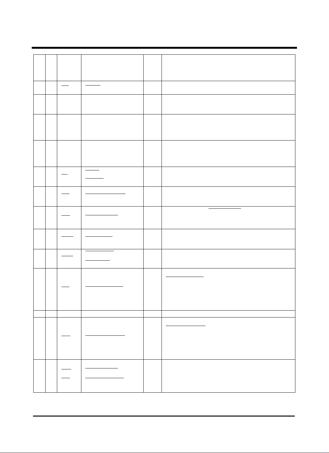
1. Pin Descriptions
1
2
3
4
5
6
7
8
9
10
GM82C765B
19
20
GM82C765B
VCC
40
39
IDX
38
TROO
WP
HDL
MO2. DS4
MO1, DS3
DS2
VSS
DS1
STEP
DIRC
WD
WE
HS
PCVAL
CLK1
DRV
CLK2
RPM, RWC
DCHG
WP
TROO
IDX
VCC
RD
WR
CS
A0
CACK
TC
36
35
34
33
26
25
38 39
37
40
42
1
2
3
4
5
6
7 8 9 10 11 12 13 14 15 16 17
DBO
DB1
GM82C765B PL
DB2
DB4
DB3
DB5
DB6
DB7
DMA
DCHGEN
IRQ
HS
PCVAL
XT1
XT1
DRV
XT2
XT2
22
RDD
21
RST
20
LDCR
18
LDOR
PIN NO
DIP PLCC
1 1
2 2
3 3
MNEMOMIC SIGNAL NAME I/O
RD
WR
CS
A0 ADDRESS LINE I
4 4
DACK
5 5
(condinued on next page)
READ
WRITE
DMA
SELECTCHIP
FUNCTION
I
Control Signal for transfer of data or status onto the
ST
data bus by the GM82C765B
I Control signal for latching data form the bus into the
GM82C765B buffer register.
ST
Selected when 0 (Low) allowing RDorWR
operation from the host
Address line selecting data (=1) or status (=0)
ST
information
(A0 = Logic 0 during WR is illegal)
I
Used by the DMA Controller to transfer data from
ST
EACKNOWLEDG
the GM82C765B onto the bus. Logical equivalent to
CS
signal is qualified by DMAEN from the Operation
Register.

3
PIN
DIP PLCC
6 6 TC
7-14 7-14
15
16
15 DMA
16 IRQ
17
17
18
19
20
18
19
20 RST RESET
21 RDD
22 2XT 2XTAL
23 XT2 XTAL2
21
(condinued on next page)
MENMO
-MIC
SIGNAL
NAME
TERMINAL
COUNT
DBO thru
DB7
DATA BUS 0
Thru
DATA BUS 7
DIRECT
MEMORY
ACCESS
INTERRUPT
REQUEST O BI
DISK
CHANGE
ENABLE
LOAD
OPERATIONS
REGISTER
LOAD
CINTROL
REGISTER
DATA
DISKREAD
DCHGEN
LDOR
LDCR
CLK2 CLOCK2
I/O
FUNCTION
This signal indicates to GM82C765B that data transfer is
complete. If DMA operational mode is selected for
command execution, TC will be qualified by
not in the programmed I/O execution. In PC AT or Special
mode, qualification by
I
mode, qualification by
ST
resister signal DMAEN to be logically true. Note also that
in PC AT mode, TC will be qualified by
requires the Operations
DACK
requires the operations
DACK
DACK
DMA or non-DMA host operation. programmed I/O in PC
AT mode will cause an abnormal termination error at the
completion of a command.
8-Bit bi-directional, tri-state, data bus.
I/O
D0 is the least significant bit (LSB).
BI
D7 is the most significant bit (MSB)
DMA request for byte transfer of data.
O
In Special or PC AT mode, this pin is tristated, enabled by
BI
the DMAEN signal from the Operation Register. This pin is
driven in the Base mode.
Interrupt request indicating the completion of command
execution or data transfer requests (in non DMA mode).
Normally driven in base mode. In special or PC AT mode,
this pin is tri-stated, enabled by the DMAEN signal from the
Operations Resister.
This input must be at logic = 0 to enable
I
status at pin 40 to be placed on DB7 during a RD = 0 of
ST
= 0. Internal pull-up.
LDCR
Address decode which enables the loading of the Operations
I
Resister. Internally gated with WR creates the strobe
ST
which latches the two LSBS from the data bus into the
Operation Resister.
Address decode which enables the loading of the Control
I
Resister. Internally gated with WR creates the strobe
which latches the two LSRs from thedata bus into the
ST
Control Resister.
Reset controller, placing microsequencer in idle. Resets
I
device outputs. Puts in base mode, not PC AT or Special
ST
mode.
This is the raw serial bit stream from the disk drive. Each
I
falling edge of the pulses represents a flux transition of the
ST
encoded data.
O N XTAL oscillator drive output for 44 pin PLCC should be
left floating if TTL inputs used at pin 23.
I N XTAL oscillator input used for non-standard data rates. It
may be driven with a TTL level signal
TTL level clock input used for non-standard data rates is
I
9.6MHz for 300 kbs, and can only be selected from the
N
Control Register. * XT2 (PIN23) of 44 pin-PLCC
GM82C765B
, but
DACK
, whether in
input
DCHG
4
22 24 DRV DRIVE TYPE
25
1XI
1XTAL
26 XT1 XTAL1
23 CLK1 CLOCK1
24 27 PCVAL
25 28
26 29
27 30
28 31
29 32
30 33
HS
WE
WD
DIRC DIRECTION
STEP
PRECOMPEN-SATION
VALUE
HEAD
SELECT
1DS
PULSESTEP
CONTROL
ENABLEWRITE
DATAWRITE
1SELECTDRIVE
31 34 VSS GROUND Ground
32 35
33 36
2DS
,
1MO
3DS
2SELECTDRIVE
1ONMOTOR
3SELECTDRIVE
I
ST
O
ST
I
N
I
N
I
ST
O
HCD
O
HCD
O
HCD
O
HCD
O
HCD
O
HCD
O
HCD
O
HCD
GM82C765B
Drive type input indicates to the device that a two-speed
spindle motor is used if logic is O. In that case, the
second clock input will never be selected and must be
grounded.
XTAL oscillator drive output for 44 pin PLCC should
be left floating if TTL inputs used at pin 26.
XTAL oscillator input requiring 16MHz crystal. This
oscillator is used for all standard data rates, and may be
driven with a TTL level signal.
TTL level clock input is used to generate all internal
timings for standard data rates. Frequency must be
16MHz ± 0.1%, and may 40/60 or 60/40 duty cycle.
*
XT1 (PIN 26) of 44-PLCC
PRECOMPENSATION VALUE select input. This pin
determines the amount of write precompensation used
on the inner tracks of the diskette. Logic 1 = 125nS,
Logic 0 = 187nS
High Current drive (HCD) output selects the head (side)
of the floppy disk that is being read or written. Logic 1
= side 0. Logic 0 = side 1.
This HCD output becomes true, active low, just prior to
writing on the diskette. This allows current to flow
through the write head.
This HCD output DATAWRITE . Each failing edge of
the encoded data pulse stream causes a flux transition
on the media.
This HCD output determines the direction of the HEAD
step motor. Logic 1 = outward motion. Logic 0 =
inward motion.
This HCD output issues an active low pulse for each
track to track movement of the head.
This HCD output, when active low, is
1SELECTDRIVE in PC AT mode, enables the interface
in disk drive. This signal comes from the Operations
Register. In Base or Special mode, this output is #1 of
the four decoded Unit Selects, as specified in the device
command syntax.
This HCD output, when active low, is
2SELECTDRIVE in PC AT mode, enables the
interface in disk drive. This signal comes from the
Operations Register. In Base or Special mode, this
output is # 2 of the four decoded Unit Selects, as
specified in the device command syntax.
This HCD output, when active low, is MOTOR ON
enable for disk drive #1, in PC AT mode. This signal
comes from the OPERATIONS Register in the BASE or
Special mode, this output is #3 of the four decoded Unit
Selects as specified in the device command syntax.

5
MNEMOMIC
PIN NO
DIP PLCC
34 37
2MO
4DS
SIGNAL NAME I/O
,
O
2 ON MOTOR
4SELECT DRIVE
This HCD output, when active low, is MOTOR ON
HCD
enable for disk drive #2, in PC AT mode. This signal
comes from the Operations Reg. In the Base or Special
mode, this output is #4 of the four decoded Unit
Selects as specified in the device command syntax
35 38 HDL HEAD
LOADED
36 39
RWC
RPM
REDUCED
WRITE
MINUTE PER
,CURRENT
SREVOLUTION
O
This HCD output, when active low, causes the head to
HCD
be loaded against the media in the selected drive.
O
This HCD output, when active los, causes a
HCD
REDUCED CURRENT WRITE
increased toward the inner tracks, becoming active
when tracks>28 are accessed. This condition is valid
for Base or Special mode, and is indicative of when
write precompensation is necessary. In the PC AT
mode, this signal will be active when CR0=1
40
DCHG
DISK
CHANGE
I
This ST input senses status from the drive, indicating
ST
active low that drive door is open or that the diskette
has possibly changed since last drive selection.
37 41 WP WRITE
PROTECTED
38 42
00TR
00 TRACK
I ST
I
This Schmitt Trigger (ST) input senses status from the
disk drive, indicating active low when a diskette is
WRITE PROTECTED
This ST input senses status from disk drive indicating
ST
active low when the head is positioned over the
outermost track,
39 43 IDX
INDEX
I
ST
This ST input senses status from the disk drive,
indicating active low when the head is positioned over
the beginning of a track marked by an index hole.
40 44 VCC +5V DC Input power supply.
Note: N – NORMAL INPUT, OUTPUT PAD
BI – BIDIRECTIONAL I/O PAD
ST – SCHMITT TRIGGER INPUT PAD
HCD – OPEN DRAIN HIGH CURRENT DRIVE OUTPUT PAD
FUNCTION
when bit density is
00 TRACK
GM82C765B

6
2. Electrical Specifications.
2.1 Absolute Maximum Ratings
— OPERATING TEMPERATURE …………………...……………………. 0°C (32°F) to 70°C (158°F)
— STORAGE TEMPERATURE ………………………………………-55°C (-67°F) to +125°C (257°F)
— VOLTAGE on any pin with respect to ground …………………………. –0.3 V to Vcc +0.3V
— SUPPLY VOLTAGE with respect to ground ……………………………………………. 7.0V
2.2 DC ELECTRICAL CHARACTERISTICS
NOTE: Maximum limits indicate where permanent device damage occurs.
Continous operation at these limits is not intended and should be limited to those conditions specified in the DC operating Characteristics
DC Operating Caracteristics: )F32( C0T
A
SYMBOL PARAMETER MIN MAX UNITS
V +5V DC POWER SUPPLY 4.5
CC
VIL Input LOW Voltage-DATA BUS & XTOSC
VIH Input HIGH Voltage-DATA BUS & XTOSC 2.0
VILT
VIHT Input HIGH Threshold Voltage-Schmitt Trigger
VOL Output LOW-DBX, IRQ, DMA: lo=12.0mA
VOH Output HIGH-DBX, IRQ, DMA: lo=-5.0mA 2.8
VOLHC Output LOW-HIGH CURRENT: lo=48mA
ILUL Latch up CURRENT LOW 40.0
ILUH Latch up CURRENT HIGH -40.0
ILLX Leakage CURRENT LOW
ILHX Leakage CURRENT HIGH
ICC Supply Current-100uA source Loads
ICCHL Supply Current-5mA source Loads
PD Power Dissipation-ICC Max*
PDHL Power Dissipation-ICCHL Max*
VPQR Power Qualified Reset Threshold 2.8
NOTE:*:Includes open DRAIN High current drives at VOL=0.4V
Input LOW Threshold Voltage-Schmitt Trigger 0.8
°°= to )F158( C70 °° ; %10V5V
CC
±=
GM82C765B
5.5 V
0.8 V
V
V
2.0 V
0.4 V
V
0.4 V
mA
mA
20.0 mA
-20.0 mA
45.0 mA
95.0 mA
425.0 mA
575.0 mA
4.35 V

7
%10V
5
VCC
±+=
=
5
5
90
65
2.3 AC Timing Specifications
GM82C765B
)F32( C0TA °°= to )F158( C70 °° :
SYMBOL
t
CY
Clock Period 60
t
PH
Clock Active (High or Low) 25
t
R
Clock Rise Time (Vin 0.8 to 2.0)
t
F
Clock Fall Time (Vin 2.0 to 0.8)
t
AR
A0, CS,
t
RA
A0, CS,
t
RR
RD Width 90
t
RD
Data Access Time from RD Low
t
DF
DB To Float Delay from RD High 10
t
A0, CS,
AW
t
WA
A0, CS , DACK , LDCR , LDOR , Hold Time from WR High 0
t
WW
t
Data Set Up Time to WR High 80
DW
t
Data Hold Time from WR High 0
WD
t
RI
IRQ Reset Delay Time from RD High 0
t
WI
IRQ Reset Delay Time from WR High 0
t
MCY
DMA Cycle Time 52
t
AM
DMA Reset Delay Time from
t
MA
t
AA
DACK Width 90
t
TC
TC Width 60
t
Reset Width-TTL Driven CLK1 250
RST
t
Reset Width-Software Reset 5
SRST
t
RDD
RDD Active Time Low 40
t
WDD
WD Write Data Width Low 1/2 (TYP) MCY
t
DST
t
STU
t
STP
t
SC
(continued on next page)
Width 60
WR
Delay Time from DMA High 0
DACK
Hold & Set Up to
DIRC
Hold Time from
DSX
Active Time Low 24
STEP
Cycle Time 132
STEP
Set Up Time to RD Low 0
DACK
Hold Time from RD High 0
DACK
DACK,LDCR,LDOR
: pF 100CL
PARAMETER MIN MAX UNITS
nS
nS
nS
nS
nS
nS
nS
nS
nS
, Set Up Time to WR Low 0
nS
nS
nS
nS
nS
1MCY + 150nS
1MCY + 150nS
MCY
DACK
Low
140
nS
nS
nS
nS
nS
MCY
nS
Low 4
STEP
Low 20
STEP
MCY
MCY
MCY
MCY

8
48
uS
SYMBOL
t
IDX
IDX Index Pulse Width 2
t
STD
t
MR
RD Delay from DMA 0
t
MW
t
MRW
t
Chip Access Delay from RST Low-TTL 32
CA
t
CAS
t
XCA
t
XTS
t
TCR
t
TCW
Note: CY specifies CLK1 or XT1 period
MCY specifies MCLK period, dependent on selected data rate
WCY specifies WCLK period, dependent on selected data rate
DIRC
WR
RD or WR Response from DMA High
Chip Access Delay from
Chip Access Delay from RST-OSC XT1 at 16MHz 500
XT2 Access Delay after RST 9.6MHz 1000
TC Delay from Last DMA or IRQ, RD 0
TC Delay from Last DMA or IRQ, WR 0
2.4 AC Timing Diagrams
(1) READ Timing
A0
PARAMETER MIN MAX UNITS
Hold Time after
96
STEP
Delay from DMA 0
t
Low 40
SRST
,
.DACK,CS
t
t
t
Data Valid
t
t
t
GM82C765B
MCY
MCY
nS
nS
MCY
MCY
MCY
uS
192 MCY
384 MCY

9
WR
DATA
IRQ
Data Valid
tAW
tWW
tWA
tWD
tWI
tDW
DMA or IRQ
TC
tCR
tCW
tTC
tMCY
tMA
tAM
tAA
tMRW
tMR
tRD
tDW
tDF
tWD
Data Valid
DMA
DACK
DATA
RD
orWR
(2) WRITE Timing
(3) TERMINAL COUNT (TC) COUNTING
(4) DMA TIMING
,A0
DACK,CS
tMW
GM82C765B
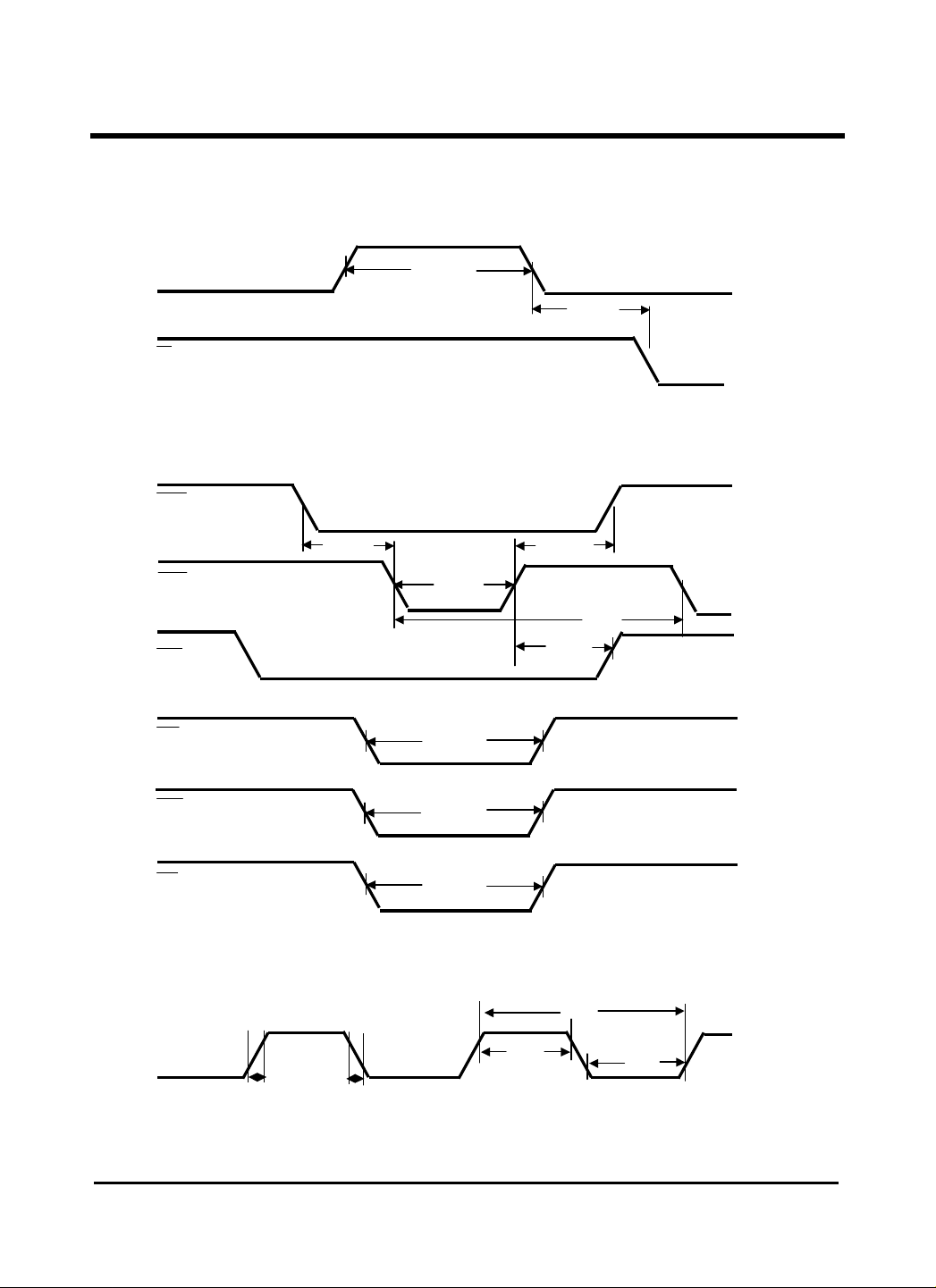
10
CS
DIRC
STEP DSX
WD
(5) RESET Timing
(6) DISK DRIVE SELECT TIMING
(7) CLOCK Timing
RESET
CLOCK
tR
tDST
tF
tRST
tSTP
tIDX
tRDD
tWDD
tPH
GM82C765B
tCA
tSTD
tSC
tSTU
tCY
tPH

11
REGISTER
STATUS REG
SEPARATOR
24 × 8
DECODE
PRECOMPENSATION
BUS
TC
DMA
IRQ
A0
CLK1
CLK2
SCLK
MCLK
WD
PCVAL
01
02
WCLK
WRCSDACK
LDCR
LDORHSSTEP
DIRC
RWC
4
1DS
−
TROOWP*
DCHG
WE
3. ARCHITECTURE
The GM82C765B Floppy Disk Subsystem
Controller is a CMOS LSI device that provides
all the needed functionality between the host
u-processor peripheral Bus and the cable
Connec-tor to the Floppy Disk Drive. This CHIP
in-tegrates; Formatter/Controller Data Separation,
Write Precompensation, Data rate Seletion,
Clock generation, Drive interface drivers and
receivers.
8 Bit
DATA
CONTROL
MASTER
HOST
INTERFACE
CLOCK
AND
TIMING
GENERATOR
ALU
MS
SATE
MACHINE
CRYSTAL
OSc×2
DIGITAL DATA
DATA ENCODER
DECODER
Fig 1. GM82C765B Internal Block Diagram
GM82C765B
HOST INTERFACE
The host interface is the host microprocessor
peripheral bus. This bus is composed of eight
control signals and eight data signals. In the
special or PC AT modes, IRQ and DMA request
are tri-stated and qualified enable, internally
provided by the operations register. The data bus,
DMA, and IRQ outputs are designed to handle 20
LS-TTL loading.
DATA
8 Bit INTERNAL DATA BUS
RAM
INSTRUCTION
PROGRAM
FLAG
CRC GENERATOR
ROM
1KÏ16
OPERATION
WRITE
DISK
INTERFACE
CONTROL
REGISTER
 Loading...