

Huntron Instruments HTR 1005B-1JS, HTR 1005B-1ES, HTR 1005B-1S User Manual
, ,
, "
OPERATOR
FOR MODELS
HTR 1005B·18 .
MANUAL
HTR 1005B·1
E8
HTR 1005B·1J8
HUNTRON INSTRUMENTS. INC
.•
15123
Hwy.
99
North.
Lynnwood. WA
98037.
(800)426-9265 • (206)743-3171 • Telex 152951

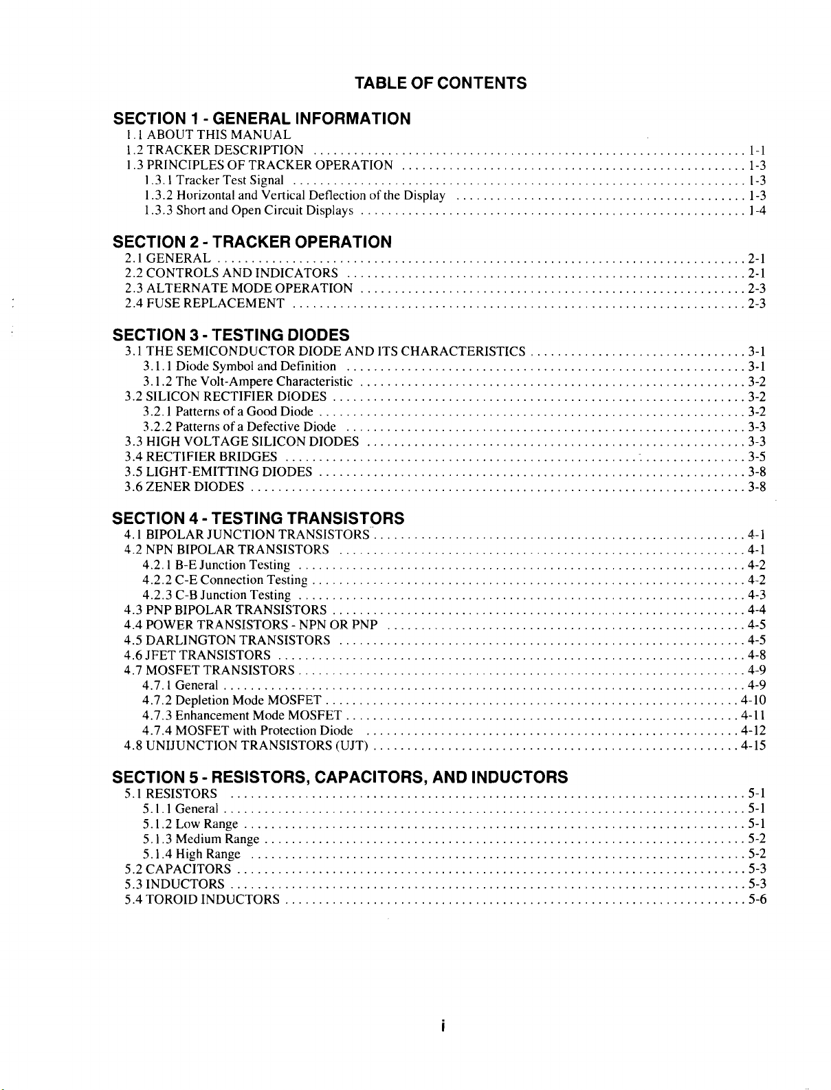
TABLE OF CONTENTS
SECTION 1 - GENERAL INFORMATION
1.1
ABOUT THIS MANUAL
1.2 TRACKER DESCRIPTION ,
1.3 PRINCIPLESOFTRACKER OPERATION ,
1.3,1 Tracker Test Signal , , , ,
1.3.2 Horizontal and Vertical Deflection of the Display " ,
1.3.3 Short and Open Circuit Displays
.",'
, ,
SECTION 2 - TRACKER OPERATION
2.1 GENERAL , , , ,
2.2 CONTROLS AND INDICATORS ,..,.,
2.3 ALTERNATE MODE OPERATION , 2-3
2.4
FUSE REPLACEMENT , ' , ' 2-3
,
SECTION 3 - TESTING DIODES
3.1
THE
SEMICONDUCTOR DIODE AND ITS CHARACTERISTICS
3.1.1 Diode Symbol and Definition
3.1.2 The Volt-Ampere Characteristic , , , 3-2
3.2 SILICON RECTIFIER
3.2.1 Patternsofa Good Diode 3-2
3.2.2 Patterns
3.3
HIGH
3.4
RECTIFIER BRIDGES , , 3-5
3.5 LIGHT-EMITTING DIODES 3-8
3.6
ZENER DIODES 3-8
ofa
VOLTAGE SILICON DIODES , , 3-3
DIODES.
Defective Diode , " 3-3
.,
, , , 3-2
, ,
1-1
1-3
1-3
1-3
1-4
2-1
2-1
3-1
3-1
SECTION 4 - TESTING TRANSISTORS
4.1 BIPOLAR JUNCTION TRANSISTORS , , , , , , , , , ,
4,2 NPN BIPOLAR TRANSISTORS
4,2.1 B-E Junction Testing
4.2.2
C-E Connection Testing , , 4-2
4.2.3
C-B Junction Testing ,
4.3
PNP
BIPOLAR TRANSISTORS , , , 4-4
4.4
POWER TRANSISTORS - NPN OR PNP 4-5
4.5 DARLINGTON TRANSISTORS
4.6
JFET TRANSISTORS , , 4-8
4.7 MOSFET TRANSISTORS , , , , , , . , ' , , , . , , 4-9
4.7. I General , , , , 4-9
4.7.2
Depletion Mode MOSFET ,
4.7.3
Enhancement Mode MOSFET 4-11
4.7.4
MOSFET with Protection Diode 4-12
4.8
UNIJUNCTION TRANSISTORS (UJT) 4-15
,'
.,
,.,.., ,
, ,
,.,
".,
',.,.,
'"
,.,
' 4-2
,.4-10
SECTION 5 - RESISTORS, CAPACITORS, AND INDUCTORS
5.1 RESISTORS
5.
1.1
General
5.1.2 Low Range 5-1
5.1.3 Medium Range 5-2
5.1.4
High Range ,
5.2 CAPACITORS 5-3
5.3 INDUCTORS , 5-3
5.4
TOROID INDUCTORS , 5-6
4-1
4-1
4-3
4-5
5-1
5-1
,.
5-2
SECTION 6 - TESTING MULTIPLE COMPONENT CIRCUITS
6.1 TRACKER DIAGNOSTIC PRINCIPLES
6.2
DIODE/RESISTOR CIRCUIT 6-2
6.2.1 Diode in Parallel with Resistor 6-2
6.2.2 Diode in Series with Resistor 6-4
6.3 DIODE AND CAPACITOR PARALLEL COMBINATION 6-5
6.4
RESISTOR AND CAPACITOR PARALLEL COMBINATION 6-7
6.5 INDUCTOR WITH DIODE 6-8
SECTION 7 - TESTING INTEGRATED CIRCUITS
7.1 INTRODUCTION
7.1.1 Integrated Circuit Technology
7.1.2 Integrated Circuit Testing Techniques 7-2
7.2 LINEAR OPERATIONAL AMPLIFIERS 7-2
7.3 LINEAR VOLTAGE REGULATORS _ 7-5
7.3.1 The 7805 Regulator 7-5
7.3.2 The 7905 Regulator 7-7
7.4
555 TIMERS 7-9
7.5 TTL DIGITAL INTEGRATED CIRCUITS 7-12
7.5.1 General 7-12
7.5.2 TTL Devices 7-13
LS
7.5.3
7.5.4
7.6
CMOS INTEGRATED CIRCITS 7-17
7.7 MICROPROCESSORS 7-19
TTL Devices 7-14
Tri-State
TTL
Digital Devices 7-15
6-1
7-1
7-1
SEC1"ION
8.1 SILICON CONTROLLED RECTIFIERS
8.2 TRIAC DEVICES 8-3
8 - TESTING RECTIFIERS
SECTION 9 - TESTING POWER SUPPLIES
9.1 GENERAL
9.2
TESTING PROCEDURE 9-2
SECTION 10 - TESTING COMPONENTS BY COMPARISON
10.1 INTRODUCTION
10.2 SETUP PROCEDURES
10.3 HIGH VOLTAGE TRANSISTOR (TIP-50) _ 10-2
10.3.1 TIP-50 B-E Junction 10-2
10.3.2 TIP-50 C-E Junction 10-3
10.4 HIGH VOLTAGE DIODE HV-15F 10-4
lOOuF
10.5
10.6 1458 DUAL OP-AMP 10-5
10.7 7905 NEGATIVE REGULATOR 10-8
25V ELECTROLYTIC CAPACITOR 10-4
SECTION11- SOLVING BUS PROBLEMS
11.1 INTRODUCTION
11.2 STUCK WIRED-OR BUS
11.3 DEFECTIVE WAVESHAPE ON BUS
11.4 MEMORIES
SECTION 12 - TROUBLESHOOTING TIPS
8-1
9-1
10-1
10-1
11-1
11-1
11-1
11-1
APPENDIX A
APPENDIX B
AI
AS
ii
SECTION 1
GENERAL
INFORMATION
1.1
ABOUT
This manualisprovided for the operatorofthe Huntron
Tracker. The information contained within this manual
familiarizes the reader first with the tracker and its principles
of
operation. and then with its specific uses. A working
knowledge
assists the user
when using the instrument for troubleshooting purposes.
The manual
information pertinent to a certain application
sections contain the following information.
Section I
This section provides a description
lists its specifications.
on which the tracker operates. using a pure resistance
and a diode as examples.
Section 2
This section describes the front panel controls
tracker.
testing feature.
THIS
of
the tracker's operating principles greatly
in
is
divided into sections. Each section contains
- GENERAL INFORMATION
- TRACKER OPERATION
It
MANUAL
evaluating the tracker's display. especially
of
of
the tracker and
It
also describes the principles
also describes the tracker's comparative
the unit. The
of
the
across) circuits containing the following devices: NPN
PNP
and
transistors,
transistors.
Section 5 - PASSIVE COMPONENTS
This section describes and illustrates tracker displays
produced when the test leads are connected to capacitive, inductive, and resitive circuits
Section 6
This section covers the testing
nations. diode/capacitor combinations. and capacitor/resistor combinations.
Section 7
This section discusses integrated circuit technology
followed
as operational amplifiers and voltage regulators. Testing information
as
well
Section 8 - TESTING RECTIFIERS
transistors, Darlington pairs, germanium
MOSFET's,
- TESTING MULTIPLE COMPONENT CIRCUITS
- TESTING INTEGRATED CIRCUITS
by
testing information for linear devices such
is
also provided for the LM555 Timer
as TTL. LS TTL, and CMOS devices.
J-FET's,
and unijunction
or
devices.
of
diode/resistor combi-
Section 3 - DIODE TESTING
This section describes the characteristics
(showing
essential to understanding the tracker display. This
section also illustrates and describes tracker displays
produced when the test leads are connected to (or
across) circuits containing the following devices: silicon diodes. high voltage silicon diodes, zener diodes,
bridging diodes. and light-emitting diodes.
Section 4
This section illustrates and describes tracker displays
produced when the test leads are connected to (or
its
voltage-to-current relationship). which
-
TRANSISffiR
TESTING
of
the diode
This section describes the testing
rectifiers and TRIAC devices.
Section 9 - TESTING POWER SUPPLIES
is
This describes how to use the tracker
transformer/full-wave bridge type'power supply.
Section
10
-TESTINGCOMPONENTSBYCOMPARISON
This section provides tracker displays for defective
components as compared to known good devices. The
tracker
voltage transistor. a high voltage diode, an electrolytic
capacitor, an op-amp, and a regulator.
is
used in the alternate mode to check a high
of
silicon-controlled
to
test the typical
1-1

SECfION11- SOLVING BUS PROBLEMS
This section contains information that may be helpful
when attempting to isolate faults caused
devices connected to a common bus.
SECfION12- TROUBLESHOOTING TIPS
by
defective
Table I-I. Specifications
of
This section contains a series
troubleshooting suggestions and information that should assist the user
when using the tracker.
TEST SIGNAL
DATA
Waveform Type sinusoidal
Frequency 80Hz
Voltage/Current Characteristics
Open Circuit Voltage (peak-to-peak)
- Low Range
20
Short Circuit Current (mA rms) 64
Power (mW rms)
Power (mW peak)
Short Circuit Current (mA peak)
81
161
170
Voltage/Current Characteristics - Medium Range
Open Circuit Voltage (peak-to-peak)
40
Short Circuit Current (mA rms) 0.27
Power (mW rms) 0.23
Power (mW peak) 0.45
Short Circuit Current (mA peak)
0.7
Voltage/Current Characteristics - High Range
Open Circuit Voltage (peak-to-peak)
120
Short Circuit Current (mA rms) 0.29
Power (mW rms) 0.26
Power (mW peak) 0.52
Short Circuit Current (mA peak) 0.8
of
NOTE: All power ratings are conditions existing across a single silicon diode in the test terminals
the tracker.
CRT SCREEN SIZE 7cm diagonal
CRT ACCELERATION POTENTIAL
1350Y
regulated
INPUT PROTECTION
Protection provided against damage caused
by
touching probestoline voltages.
TRACE ALTERNATE MODE
Alternates display between channel A and B inputs at o.8Hz rate
POWER REQUIREMENTS
HTR l005B-IS
HTR
l005B-1
ES 220/240V, SO/60Hz
HTR l005B-IJS
IOOY,
50/60Hz
117V,60Hz
WEIGHT 5 pounds, 5 ounces
DIMENSIONS (inches)
3
8-
/4
W X
(21.9 em x 7.4
3-1/2
H X
emx24.2cm)
AMBIENT TEMPERATURE
Operating . zero to + 50 degrees Celsius
Storage -50 to
+60
degrees Celsius
SHOCK AND VIBRATION
Will withstand shock and vibration encountered
in
commerical shipping and handling
1·2
(2.4 kg)
11-1/2
D
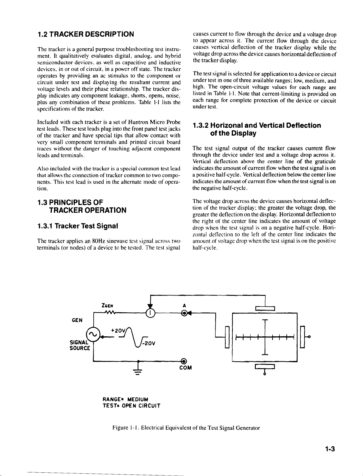
1.2 TRACKER DESCRIPTION
The tracker is a general purpose troubleshooting test instrument. It qualitatively evaluates digital, analog, and hybrid
semiconductor devices, as well as capacitive and inductive
devices, in or out ofcircuit,
operates
circuit under test and displaying the resultant current and
voltage levels and their phase relationship. The tracker display indicates any component leakage, shorts, opens, noise,
plus any combination of these problems. Table
specifications ofthe tracker.
by
providing an ac stimulus to the component or
in
a power off state. The tracker
I-I
lists the
causes current to flow through the device and a voltage drop
to appear across
causes vertical deflection
voltage drop across the device causes horizontal deflection
the tracker display.
The test signal is selected for appl ication to a device
under test
high. The open-circuit voltage values for each range are
listed
each range for complete protection
under test.
in
in
Table
it.
The current flow through the device
of
the tracker display while the
oneofthree available ranges;
1-1.
Note that current-limitingisprovided on
low,
of
the deviceorcircuit
or
circuit
medium, and
of
Included with each tracker is a set
test leads. These test leads plug into the front panel test jacks
of
the tracker and have special tips that allow contact with
very small component terminals and printed circuit board
traces without the danger
leads and terminals.
Also included with the tracker is a special common test lead
that allows the connection oftracker common to two components. This test lead
tion.
of
is
usedinthe alternate modeofopera-
of
Huntron Micro Probe
touching adjacent component
1.3 PRINCIPLES OF TRACKER OPERATION
1.3.1 Tracker Test Signal
The tracker applies an 80Hz sinewave test signal across two
terminals (or nodes) of a device to be tested. The test signal
1.3.2 Horizonal and Vertical Deflection
of
the
Display
The test signal outputofthe tracker causes current flow
through the device under test and a voltage drop across it.
Vertical deflection above the center line
indicates the amount
a positive half-cycle. Vertical deflection below the center line
indicates the amount
the negative half-cycle.
The voltage drop across the device causes horizontal deflec-
of
the tracker display; the greater the voltage drop, the
tion
greater the deflection on the display. Horizontal deflection to
the right
drop when the test signal is on a negative half-cycle. Horizontal deflection
amount of voltage drop when the test signal is on the positive
half-cycle.
of
the center line indicates the amountofvoltage
of
current flow when the test signal is on
of
current flow when the test signal is on
to
the left of the center line indicates the
of
the graticule
GEN
ZiEN
+25"\_
RANGE-
TEST-
OPEN
Figure
V~20V
COM
MEDIUM
CIRCUIT
I-I.
Electrical Equivalentofthe Test Signal Generator
1-3
Figure
generator within the tracker and
voltage drop across the test terminals provide vertical and
horizontal deflectionofthe display. The 80Hz test signal is
providedbythe signal generator and
(Zgen). All current that passes through the test terminals to
the device under test, also passes through a current sensing
point (I). The vertical deflection plates receive deflection
voltage from this current sensing point. The amount
deflection voltage provided to the vertical deflection plates is
proportional to the amountofcurrent flowing through the
device under test.
The voltage appearing across the test terminals (and the
device undertest)isalso applied across the horizontal deflection plates. The amountofvoltage provided to the horizontal
deflection plates is proportional to the voltage drop across the
device under test.
I-I
shows the electrical equivalentofthe test signal
how
the current through and
its
series impedance
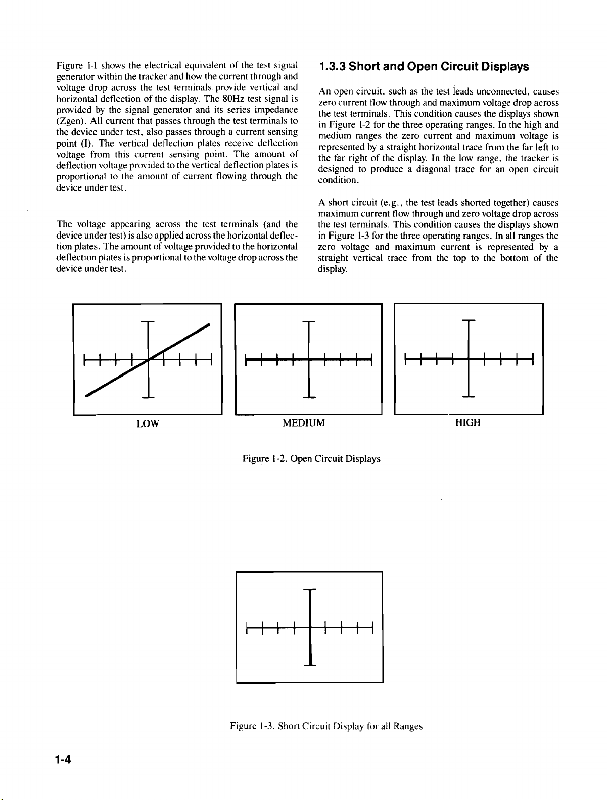
1.3.3 Short and Open Circuit Displays
An open circuit, such as the test ieads unconnected, causes
zero current flow through and maximum voltage drop across
the test terminals. This condition causes the displays shown
in
Figure
1-2
for the three operating ranges.Inthe high and
medium ranges the zero current and maximum voltage
representedbya straight horizontal trace from the far left
of
the far right of the display.Inthe low range, the tracker
designed to produce a diagonal trace for an open circuit
condition.
A short circuit (e.g., the test leads shorted together) causes
maximum current
the test terminals. This condition causes the displays shown
in
Figure
1-3
zero voltage and maximum currentisrepresented
straight vertical trace from the top to the bottomofthe
display.
flow
through and zero voltage drop across
for the three operating ranges.Inall ranges the
by
is
to
is
a
LOW
Figure 1-2.
MEDIUM
Open
Circuit Displays
HIGH
1-4
Figure 1-3. Short Circuit Display for all Ranges
GEN
320
PEAK
JAQ
A
+---
+2~
'
20-
"V
SIGNAC
SOURCE
COM
RANGE:MEDIUM
TEST: 33K
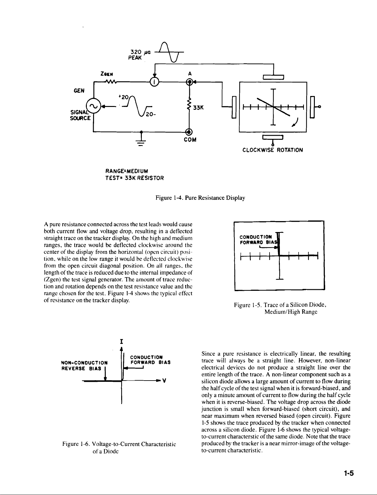
A pure resistance connected across the test leads would cause
both current flow and voltage drop, resulting
straight trace on the tracker display. On the high and medium
ranges, the trace would be deflected clockwise around the
center
of
the display from the horizontal (open circuit) position, while on the low range it would be deflected clockwise
from the open circuit diagonal position. On
of
length
(Zgen) the test signal generator. The amount of trace reduction and rotation depends on the test resistance value and the
range chosen for the test. Figure
of
the traceisreduced due tothe internal impedance
resistance on the tracker display.
RESISTOR
Figure 1-4. Pure Resistance Display
in
a deflected
all
ranges, the
1-4
shows the typical effect
of
33K
CLOCKWISE
T
Figure 1-5. Trace
Medium/High Range
)
ROTATION
of
a Silicon Diode,
I
CONDUCTION
NON-CONDUCTION
REVERSE
Figure 1-6. Voltage-to-Current Characteristic
--
BIAS
ofa
....
-(------..v
Diode
FORWARD
BIAS
Since a pure resistanceiselectrically linear, the resulting
be
trace will always
electrical devices do not produce a straight line over the
entire length
silicon diode allows a large amount
the halfcycle
only a minute amount
when
junction
near maximum when reversed biased (open circuit). Figure
1-5
shows the trace producedbythe tracker when connected
across a silicon diode. Figure
to-current characterstic
produced
to-current characteristic.
of
of
itisreverse-biased. The voltage drop across the diode
is
small when forward-biased (short circuit), and
by
the trackerisa near mirror-imageofthe voltage-
a straight line. However, non-linear
the trace. A non-linear component such as a
of
current to flow during
the test signal when itisforward-biased, and
of
current to flow during the halfcycle
1-6
shows the typical voltage-
of
the same diode, Note that the trace
1·5

NOTES:
1-6

2.1
GENERAL
2.2
CONTROLS
SECTION 2
TRACKER
OPERATION
AND
INDICATORS
Components are testedbythe tracker using a two terminal
system, where two test leads are placed across the component
is
under test. All testing
tions for the component/equipment under test. The tracker
tests components while in-circuit, even when bridged
other components. Included with each trackerisa set of
Huntron Micro Probe test leads. Also included with the
is
tracker
tion
usedinthe alternate modeofoperation.
a special common test lead that allows the connec-
of
tracker common to two components. This test lead
performed under power-off condi-
by
1
2
3
+
Operationofthe tracker, for the mostpart, amounts to deter-
of
mining the significance
display. While the tracker
panel contoIs to assist
of
these controlsisnecessary to during actual useofthe
use
2-1
tracker. Table
and Figure
sis on tracker operation is on the determination
displays. For this reason, the majority
is
in
tained
4
this documentisrelative to tracker displays.
5
lists and describes the front panel controls,
2-1
shows the control,although the main empha-
6
the trace(s) appearing on the
is
equipped with several front
in
optimizing displays, only limited
of
information con-
7
8
9
10
of
tracker
15 14
Figure 2-1. LocationofFront Panel Controls
13
12
11
2·1
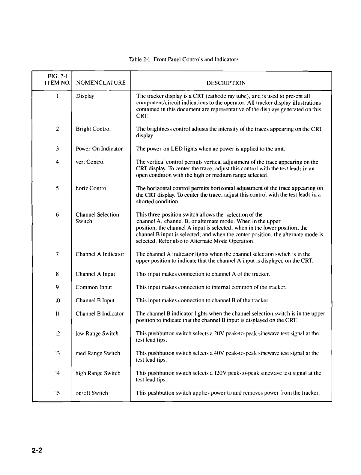
Table
2-1.
Front Panel Controls and Indicators
FIG.
2-1
ITEM
NO.
NOMENCLATURE
DESCRIPTION
1 Display The tracker display is a CRT (cathode ray tube), and is used to present all
component/circuit indications to the operator. All tracker display illustrations
of
contained in this document are representative
CRT.
the displays generated on this
2
3 Power-On Indicator The power-on
4 vert Control
5
6
7
8
9
10
Bright Control
horiz Control
Channel Selection This three-position switch allows the selectionofthe
Switch
Channel A Indicator
Channel A Input
Common
Channel B Input
Input
The
brightness control adjusts the intensityofthe traces appearing on the CRT
display.
The
vertical control permits vertical adjustmentofthe trace appearing on the
CRT display.
open condition with the high
The
horizontal control permits horizontal adjustmentofthe trace appearing on
the CRT display.
shorted condition.
channel A, channel B,
position, the channel A input
channel B input
selected. Refer also to Alternate Mode Operation.
The
channel A indicator lights when the channel selection switchisin
upper position to indicate that the channel A input
This input makes connection to channel A
This input makes connection to internal common
This input makes connection to channel B
LED
lights when ac power is applied to the unit.
To
center the trace, adjust this control with the test leads in an
or
medium range selected.
To
center the trace, adjust this control with the test leads in a
or
alternate mode. When in the upper
is
selected; when in the lower position, the
is
selected; and when the center position, the alternate mode
is
displayed on the CRT.
of
the tracker.
of
the tracker.
of
the tracker.
is
the
2-2
11
12
13
14
15
Channel B Indicator
low Range Switch
med Range Switch
high Range Switch
on/off
Switch
is
The channel B indicator lights when the channel selection switch
position to indicate that the channel B input
This pushbutton switch selects a 20Y peak-to-peak sinewave test signal at the
test lead tips.
This pushbutton switch selects a 40Y peak-to-peak sinewave test signal at the
test lead tips.
This pushbutton switch selects a 120Y peak-to-peak sinewave test signal at the
test lead tips.
This pushbutton switch applies power to and removes power from the tracker.
is
displayed on the CRT.
in the upper
2.3
ALTERNATE MODE OPERATION
2.4
FUSE REPLACEMENT
The tracker can alternate automatically between the displays
of
the channel A and channel B inputs. This allows the user to
of
directly compare the display
known good circuit for quality assurance operations,
troubleshooting purposes. Figure 2-2 shows how a tracker
connected to compare a known good board with a board
under test. This testing mode utilizes the dual common test
lead supplied with the unit and alternates between the channels at a 0.8 Hz rate.
THE
CAUTION:
HAVE POWER
VOLTAGE CAPACITORS
BEFORE CONNECTING
SYSTEM m BE
TURNED
the suspect circuit to thatofa
CHECKED
OFF,
AND
HAVE
ALL
THE
FULLY
TRACKER
DISCHARGED
or
for
MUST
HIGH
The tracker contains a 0.25 ampere fuse
series with the channel A and B input leads. Accidental
contact
sources, will blow this fuse, making replacement necessary.
is
When FI fails
the CRT from a horizontal
WARNING: REPLACEMENT
BE PERFORMED
NELONLY.
To
replace the fuse, disconnect the tracker from the ac power
source. Remove the four cover retaining screws located on
the bottom
position, lift off the top cover to expose the interior
unit. Locate
immediately behind the power switch, and replace with a
0.25A, 250V, type AGX.
(Fl)
connected in
of
the leads to charged capacitorsorother voltage
it
will not be possible to deflect the pattern on
or
diagonal line.
OF
THE
FUSE SHOULD
BY
QUALIFIED SERVICE PERSON-
of
the unit. Holding the tracker in an upright
Fl
on the main printed circuit board assembly
CHANNEL
SELECTION
SWITCH
CHANNEL A
L.E.D.
RED
TEST
TERMINAL
of
the
+
BLACK
MICROPROBE
BLACK
TEST
TERMINAL
YELLOW
TEST
TERMINAL
CHANNEL B
L.E.D.
Figure 2-2. Comparing a Known Good Board With a Defective Board
2·3

NOTES:
2-4
SECTION 3
TESTING DIODES
3.1
THE
SEMICONDUCTOR DIODE
AND ITS CHARACTERISTICS
3.1.1
Diode Symbol and Definition
A semiconductor diode is formed into a diodebythe creation
of
a junction between P-material and N-material within a
of
crystal during the process
semiconductor diode has in its symbol, an arrow to indicate
of
the direction
forward current
manufacture. The standard
flow,
as showninFigure
3-1.
+~-
Figure 3-1. Diode Symbol
With positive voltage applied to the P-junction and negative
voltage applied to the N-junction, the diodeissaid to be
forward biased, as shown in Figure 3-2. The current (It)
increases rapidly with small increases in applied voltage (V).
When the applied voltage is reversed, the P-junction is negative with respect to the N-junction, and very small levels
current flow through the diode. Figure 3-3 shows the P-N
junction in the reverse bias mode. The small current
the diode "reverse saturation
increases with temperature.
current",
In
practice,10can be ignored.
and its magnitude
(10) is
METAL
CONTACTS
p
N
of
Figure 3-2. P-N Junction Biased in the
Forward Direction
+
Figure 3-3. P-N Junction Biased
Reverse Direction
in
the
3·1
3.1.2
The
Volt-Ampere Characteristic
3.2 SILICON RECTIFIER DIODES
Fora P-N junction, the current (I)isrelated to the voltage (V)
by
the following equation:
= lo(exp
I
Where kisa constant depending on the temperature and
material. The volt-ampere characteristic described
equation above
the current
The dashed portion
at a certain reverse voltage (Vbr), the diode characteristic
exhibits an abrupt and marked departure from the equation
At
above.
and the diode
REVERSE
BIAS
kV
-1)
by
the
is
showninFigure 3-4. For the sake of clarity,
(10) has been greatly exaggerated
of
the curveofFigure 3-4 indicates that,
this critical voltage, a large reverse current flows
is
said tobein
the "breakdown region" .
I
in
magnitude.
FORWARD
BIAS
V
Patternsofa Good Diode
3.2.1
A good diode has very large reverse-biased resistance and
small forward-biased resistance. The forward junction volt-
is
age drop (Vf)
on the semi-conductor material; for example, Vf for a silicon
is
diode
volts. The tracker can visually display all these parameters.
Figure 3-5 shows the tracker-diode connections for diode
testing. Figure 3-6 shows typical patterns
high ranges) and waveforms. plus the circuit equivalent,for a
good silicon diode
drop
range display.
0.6 volts; and for a typical light-emitting diode,is1.5
of
a diode can be determined (approximately) from
between 0.5 volts and 2.8 volts, depending
(low,
medium, and
(I
N4OOl).
The forward junction voltage
A
(-J*-----.
COM
low
D
Figure 3-4. The Volt-Ampere Characteristic
of
a Semiconductor Diode
INPUT WAVEFORM
LOW
..
--~..-
CIRCUIT EQUIVALENT
MEDIUM
.....
Figure 3-5. Tracker Test Circuit
r=v
OUTPUT WAVEFORM
HIGH
3-2
Figure 3-6. Waveforms and Typical Patterns - Good Silicon Diode
3.2.2 Patterns of Defective Diodes
A rectifier diodeisdefectiveifitisopen,isshorted (low
impedance), contains high internal impedance, or contains
3-7
leakage. Figure
the
low,
medium, and high ranges.
The tracker
ance higher than one ohm, and this resistance causes the
vertical line to rotate in a counterclockwise direction. The
angle
of
rotationisa functionofthe resistance. Figure 3-8
shows the effect
in
while
does not cause rotation in the medium and high ranges
tracker.
Figure
waveforms
the low range. This small short-circuit resistance
3-9 shows the waveforms, circuit equivalent and
of
shows the patterns ofan "open" diode
is
capable, in the low range, ofdetecting resist-
of
circuit resistances on the trace rotation
of
a diode that exhibits a non-linear resistance in
the
series with the diode junction. This resistance effects the
ability ofthe diode to turn-on at the proper voltage.
3-10
Figure
waveforms ofa diode that exhibits a non-linear resistance
in
parallel with the diodejunction (leaky) when reverse-biased.
This resistance effects the ability
maximum output for a given input.
3.3
HIGH
High voltage diodes are tested in the same manner as that
described for rectifier in section 3.2. High voltage diodes,
such as the HV l5F, display higher forward voltage drop (Vf)
than the rectifier diodes described in section
shows the patterns of the HV15F high voltage diode. The
for the high voltage diode is higher on all tracker ranges than
that
of
shows the waveforms, circuit equivalent and
of
the diodetoprovide
VOLTAGE
a regular diode.
SILICON DIODES
3.2. Figure
in
3-11
Vf
LOW
Figure
MEDIUM
3-7. Patterns
ANGLE
of
an Open Diode
OF
ROTATION
HIGH
INFINITE
RESISTANCE
Figure 3-8. The EffectofDiode Short-Circuit Resistance - Low Range
3-3
INPUT WAVEFORM
Figure 3-9. Waveforms and Typical Patterns - High Impedance Diode
CIRCUIT EQUIVALENT
LOW MEDIUM
OUTPUT WAVEFORM
,..........
\.T
'-'
INPUT WAVEFORM
CIRCUIT EQUIVALENT
LOW
3-10. Waveforms and Typical Patterns - Leaky Diode
Figure
I I I I
I I I I
I I I I
I I I I
-'-
MEDIUM
OUTPUT
WAVEFORM
3-4
LOW
Figure 3-11. Pattern
MEDIUM
ofa
High Voltage Diode. HV15F
HIGH
3.4 RECTIFIER BRIDGES
A rectifier bridge assembly is made upoffour diodes confi-
in
Figure
3-12.
gured as shown
input terminals; C and D are the positive and negative output
terminals, respectively.
connected to terminals A and B as shown in Figure 3-12.
A good bridge appears as an open circuit to the tracker
because the diodes are reverse-biased. Figure
patterns produced
nected across points A and
produced
by
by
a good bridge with the tracker con-
a bridge with either diode D2orD4 shorted;
Points A and
To
test the bridge, the tracker is
B.
Figure
3-14
Bare
ac power
3-13
shows the
shows the patterns
while Figure
diode
DIorD3 shorted.
Figure
positive and negative terminals
Tracker channel A is connected to the positive terminal, and
tracker common to the negative terminal. Figure
the patterns
Figure
Figure
Figure
reversal
3-15
shows the patterns produced with either
3-16
shows the test connectionsofthe tracker to the
of
the rectifier bridge.
of
a good bridge when connected as shown in
3-16.
3-18
shows a reversalofthe test connections shown in
3-16.
Figure
3-19
shows the patterns resulting from the
of
the test connections to the bridge.
"'VA
3-17
shows
D
A
D
COM
Figure 3-12. Rectifier Bridge Test Connections - AC Input
LOW
MEDIUM
Figure 3-13. Patternsofa Good Rectifier Bridge
3·5
MEDIUM/HIGH
LOW
Figure 3-14. Patterns with D2orD4
MEDIUM/HIGH
Figure 3-15. Patterns with D 1orD3 Shorted
Shorted
LOW
3-6
A
COM
D
Figure 3-16. Rectifier Bridge Test Connections - DC Output
MEDIUM/HIGH
Figure 3-17. Patterns at Output Terminals
A
R--\--'
COM
LOW
D
Figure 3- I8.Rectifier Bridge, Reversed Test Connections
MEDIUM/HIGH
Figure 3-19. Tracker Patterns, Output Terminals Reversed
LOW
3-7
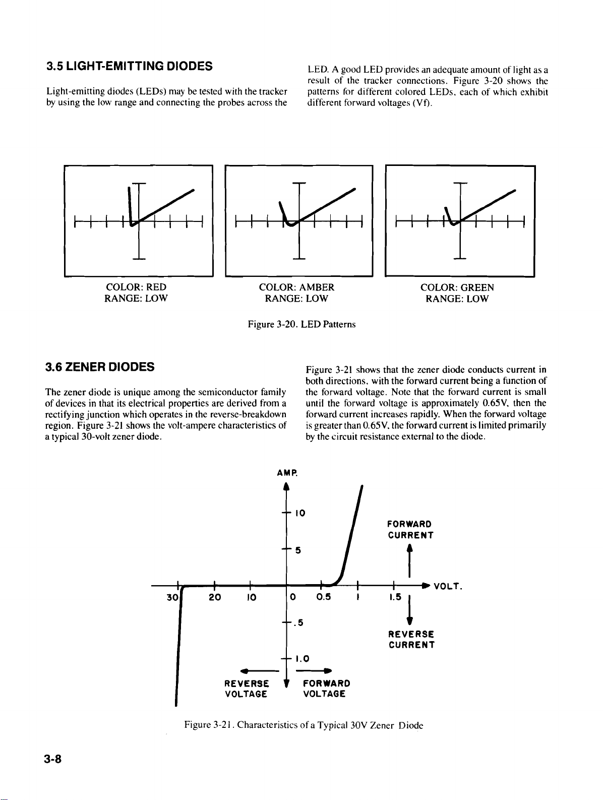
3.5 LIGHT-EMITTING DIODES
Light-emitting diodes (LEDs)
by
using the low range and connecting the probes across the
may
be tested with the tracker
an
LED. A good LED provides
of
result
patterns for different colored LEDs, each
different forward voltages (VD.
the tracker connections. Figure 3-20 shows the
adequate amount oflight as a
of
which exhibit
COLOR: RED
RANGE: LOW
COLOR: AMBER
RANGE: LOW
Figure 3-20. LED Patterns
3.6 ZENER DIODES
The zener diodeisunique among the semiconductor family
of
devicesinthat its electrical properties are derived from a
rectifying junction which operates
region. Figure
a typical 30-volt zener diode.
3-21
shows the volt-ampere characteristics
in
the reverse-breakdown
COLOR: GREEN
RANGE: LOW
Figure
both directions, with the forward current being a function
the forward voltage. Note that the forward currentissmall
of
by
AMP.
10
3-21
shows that the zener diode conducts current
is
until the forward voltage
forward current increases rapidly. When the forward voltage
is
greaterthan0.65V, the forward currentislimited primarily
the circuit resistance external to the diode.
approximately
FORWARD
CURRENT
5
O.65V,
in
of
then the
3-8
o
30
20
10
REVERSE
VOLTAGE
Figure 3-21. Characteristicsofa Typical 30V Zener Diode
0.5
.5
1.0
FORWARD
VOLTAGE
REVERSE
CURRENT
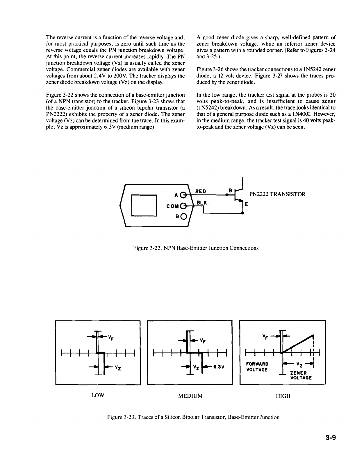
The reverse current is a functionofthe reverse voltage and,
for most practical purposes, is zero until such time as the
reverse voltage equals the PN junction breakdown voltage.
At this point, the reverse current increases rapidly. The PN
junction breakdown voltage (Vz) is usually called the zener
voltage. Commercial zener diodes are available with zener
2.4V
voltages from about
zener diode breakdown voltage (Vz) on the display.
to 200V. The tracker displays the
A good zener diode gives a sharp, well-defined pattern
zener breakdown voltage, while an inferior zener device
gives a pattern with a rounded comer. (Refer to Figures 3-24
and 3-25.)
Figure 3-26 shows the tracker connections to a 1N5242 zener
diode, a 12-volt device. Figure
duced
by
the zener diode.
3-Zl shows the traces pro-
of
Figure 3-22 shows the connectionofa base-emitterjunction
(of a NPN transistor) to the tracker. Figure 3-23 shows that
of
the base-emitter junction
PN2222) exhibits the property
voltage (Vz) can be determined from the trace. In this example, Vz is approximately 6.3V (medium range).
a silicon bipolar transistor (a
of
a zener diode. The zener
A
COM
D
Figure 3-22. NPN Base-Emitter Junction Connections
In the low range, the tracker test signal at the probes is
volts
peak-to-peak,
(1
N5242) breakdown. As a result, the trace looks identical to
that
of
a general purpose diode such as a IN4001. However,
in the medium range, the tracker test signal is
to-peak and the zener voltage (Vz) can
8
and
is insufficient to cause
be
PN2222 TRANSISTOR
E
seen.
40
volts peak-
zener
20
LOW
Figure 3-23. Traces
FORWARD
VOLTAGE
MEDIUM
of
a Silicon Bipolar Transistor, Base-Emitter Junction
HIGH
VZ~
ZENER
VOLTAGE
I
I
3·9
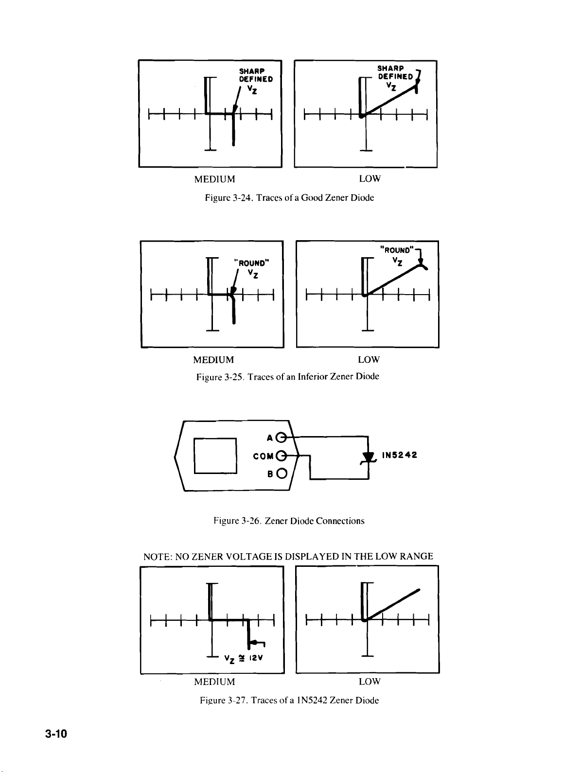
SHARP
DEFINED
V
z
MEDIUM
Figure 3-24. Traces
"ROUND"
V
z
MEDIUM
Figure 3-25. Traces
COM
D
of
a Good Zener Diode
of
an Inferior Zener Diode
A
LOW
LOW
IN!5242
3-10
Figure 3-26. Zener Diode Connections
NOTE: NO ZENER VOLTAGE
V
~
12V
z
MEDIUM
Figure 3-27. Traces
IS
DISPLAYED IN THE LOW RANGE
LOW
ofa
IN5242 Zener Diode
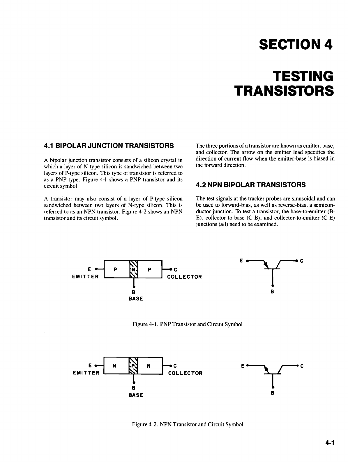
4.1
BIPOLAR JUNCTION TRANSISTORS
A bipolar junction transistor consistsofa silicon crystal
which a layerofN-type siliconissandwiched between two
layers of P-type silicon. This type
as a PNP type. Figure
circuit symbol.
4-1
of
transistorisreferred to
shows a PNP transistor and its
SECTION 4
TESTING
TRANSISTORS
of
The three portions
and collector. The arrow on the emitter lead specifies the
direction
in
the forward direction.
4.2 NPN BIPOLAR TRANSISTORS
of
current
a transistor are known as emitter, base,
flow
when the emitter-baseisbiased in
may
A transistor
sandwiched between two layers
referred to as an NPN transistor. Figure 4-2 shows an NPN
transistor and its circuit symbol.
also consistofa layer of P-type silicon
of
N-type silicon. This
~
BASE
P
__
~~O~LECTO"
B
Figure 4-1. PNP Transistor and Circuit Symbol
The test signals at the tracker probes are sinusoidal and can
be used to forward-bias, as well as reverse-bias, a semicon-
is
ductor junction.
E), collector-to-base (C-B), and collector-to-emitter (C-E)
junctions (all) need to be examined.
To
test a transistor, the base-to-emitter (B-
E
.....
-'\...
~-.c
B
E
'"
T~E-;1~_N_
.....
~~_N_""'~~LLECTO"
B
BASE
Figure 4-2. NPN Transistor and Circuit Symbol
B
4-1
4.2.1 B-E Junction Testing
The B-E junction of a transistor exhibits a zener diode
characteristic (i.e.. heavy current conduction when the B-E
is
junction
reversed-biased). Vzisapproximately 6.5 volts. Figure 4-3
forward-biased. and zener breakdown when it
COM
D
Figure 4-3. Base-Emitter Junction Connections
FORWARD
BIASED
HEAVY
I CONDUCTION
V
=
6.15V
z
shows the connection
PN2222 transistor. Figure 4-4 shows the patterns produced
is
by
the B-E junctioninthe low and medium ranges.
A
P\o-\-----~
'------
of
the tracker to
B
..
E
the
B-E junction of a
Vz
REVERSE
BI
ASE
0
MEDIUM
Figure 4-4. Base-Emitter Junction Patterns
4.2.2
Fora good transistor, the C-Econnection should appear as an
open circuit (to the tracker) when the collector voltage
positive with respect to the emitter. When the collector
voltage is negative with respect to the emitter, the transistor
goes into non-destructive breakdown at VBR.
C-E Connection Testing
COM
D
Figure 4-5 shows the connection ofthe tracker to the C and E
is
terminals
patterns produced
A
of
r-----
"'------
V
z
REVERSE
BIASED
LOW
a PN2222 transistor. Figure 4-6 shows the
by
the C-E connection in all ranges.
..... C
8
...
E
4-2
Figure 4-5. Collector-Emitter Connections - PN2222 Transistor
MEDIUM/HIGH LOW
Figure 4-6. Collector-Emitter Connection Patterns - PN2222 Transistor
4.2.3
The patternofa good C-B junction looks like thatofa diode.
Figure 4-7 shows the connection
junction
C-B Junction Testing
of
the tracker to the C-B
of
a PN2222 transistor. Figure 4-8 shows the pat-
COM
D
Figure 4-7. Collector-Base Junction Connections
terns produced
ranges.
,..-----
A
by the C-B junction
..
C
E
in
the low and medium
MEDIUM
Figure 4-8. Collector-Base Junction Patterns
LOW
4-3
4.3 PNP BIPOLAR TRANSISTORS
The testingofPNP
for NPN transistors, except that the patterns are reversed
transistorsisthe same as that described
MEDIUM
Figure 4-9. PatternofB-E Connection - MPSA92 Transistor
from their NPN equivalent. Refer to Figures 4-9,4-10, and 4-
ll.
LOW
4-4
MEDIUM
Figure 4-10. PatternofC-E
MEDIUM
Figure 4-11. Pattern
ofC-B
LOW
Connection - MPSA92 Transistor
LOW
Connection - MPSA92 Transistor
4.4
POWER TRANSISTORS - NPN ANO PNP
Transistor testing procedures described in paragraphs 4.2
and 4.3 are applicable to power transistors. However, some
in
power transistors show capacitance on the pattern
Figure 4-12. PatternofPower Transistor Showing Capacitance Loop
4.5
DARLINGTON TRANSISTORS
The Darlington transistorisbasically two transistors connected to form a composite pair as shown in Figure
of
input resistance
Darlington transistors are testedinthe same manner as NPN
Q2 constitutes the emitter load for Q
the high
LOOP
DUE
CAPACITANCE
4-13.
The
I.
range. Figure
capacitance.
TIP
TO
50
4-12
shows the loop in the pattern caused
HIGH
and PNP bipolartransistors, except that theirtrackerpatterns
differ. Figure
monly-used Darlington transistor, the TIP-Il2, and its pin
assignments.
4-14
shows the equivalent circuit of a com-
by
r---
.....
--
...... c
B
----I
Q2
E
Figure 4-13. Darlington Transistor - Schematic Diagram
r--------
o
BeE
Figure 4-14. The TIP-I12Darlington Transistor
B
....-....
I
QI
I
..
~----
-f
BI<
60
C
..........
01
E
4-5
To
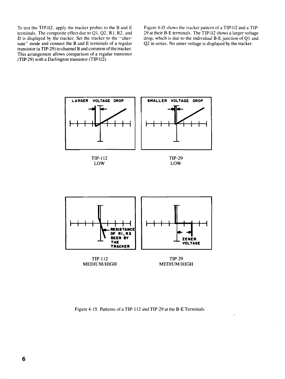
test the TIP-lI2. apply the tracker probes to the
terminals. The composite effect due to
D is displayed
nate"
mode and connect the
by
the tracker. Set the tracker to the "alter-
Band
QI,
Q2. RI. R2, and
E terminalsofa regular
transistor (a TIP-29) to channel B and common
This arrangement allows comparison
of
a regular transistor
(TIP-29) with a Darlington transistor (TIP-Il2).
ofthe
Band
tracker.
Figure
4-15
E
shows the tracker patternofa TIP-lI2 and a TIP29 at their B-E terminals. The TIP-Il2 shows a larger voltage
drop, which
Q2 in series. No zener voltage
is
due to the individual B-E junctionofQ I and
is
displayedbythe tracker.
LARGER VOLTAGE
TIP-I
12
LOW
DROP
RESISTANCE
otr
RI,
tEEN IV
TRACKER
R2
THE
SMALLER
VOLTAGE
TIP-29
LOW
DROP
TIP-Il2
MEDIUM/HIGH
Figure 4-15. Patternsofa
TIP-I12and TIP-29 at the B-E Terminals
TIP-29
MEDIUM/HIGH
6
 Loading...