

Huntron Instruments HTR 1005B-1JS, HTR 1005B-1ES, HTR 1005B-1S Service manual
OAt
Dc{]
QdJ
[N]Lr
~
Lr[22~ccgD~~~®
MAINTENANCE
FOR MODELS
HTR 10058·15
HTR 10058·1E5
(Q)[N]®
MANUAL
HTR 10058·1
J5
HUNTRON INSTRUMENTS, INC.•15123 Hwy.99North.
Lynnwood, WA
98037.
(800)426-9265 • (206)743-3171 • Telex
152951

TABLE OF CONTENTS
SPECIFICATION S................................ ................................ ................................ .................. 2
GENERAL DESCRIPTION................................ ................................ ................................ ....... 3
THEORY OF OPERATION................................ ................................ ................................ ......... 5
The Test Signal................................ ................................ ................................ ................ 5
Testing Reactive Components ................................................................ ...................... 8
CIRCUIT DESCRIPTION
Signal Section................................ ................................ ................................ .............. 10
Oscillator
................................................................ ................................ ................... 12
Power
Supply
................................................................ ................................ ............ 12
Cathode Ray TubeCircuit................................ ................................ ............................. 12
INTERNAL SETUP AND ADJUSTMENTS ................................ ................................ ................ 17
TROUBLE SHOOTING
General Information ................................ ................................ ................................ .... 19
Power Supply ................................ ................................ ................................ ............ 19
Signal Section ................................ ................................ ................................ .............. 22
CRT Section................................ ................................ .................................................... 24
Oscillator
Section................................ ................................ ................................ ....
24
LIST OFREPLACEMENT PARTS................................................................ ............................ 25
SETUP, ADJUSTMENT & SCHEMATIC FOR SERIAL# PREFIX 212 ..................................33
© COPYRIGHT 1983- HUNTRON® INST RUMENTS, INC.
HTR
1005B-1S,B-1ES,B-1JS
The information contained herein is the exclusive property of Huntron® Instruments, Inc. (except as
otherwise indicated) and shall not be reproduced in whole or in part without written authorization
fromthe company.
All information contained in this manual is the latest product information available at the time
of
printing. Huntron® Instruments, Inc. reserves the right to make changes at any time without
notice.
1
POWER REQUIREMENTS:
HUNTRON
TRACKER®
SPECIFICATIONS
HTR 1005B-1S
HTR 1005B-1ES
HTR 1005B-1JS
10
Watts
SIZE:
V'Jidth
Height
Length
WEIGHT 5 pounds 5
AMBIENT TEMPERATURE:
Operating
Storage
SHOCK AND VIBRATION:
Will
Maximum
withstand
shock
and vibration encountered in
117VAC
220/240VAC
100VAC
_ 8
commercial
shipping
'"
111/2
a
to
50
-50to60
and handling.
60Hz
50/60Hz
50/60Hz
3
,4 Inch
31/2
deg C
deg C
TEST SIGNAL DATA:
Inch
Inch
oz.
All ratings, except
terminalsofthe TRACKER® .
Waveform sine
Frequency - 80 Hz
RANGE
HIGH
MED.
LOW
CRT SCREEN SIZE 7 cm diagonal
ACCELERATION POTENTIAL 1350V. regulated
TRACE COMPARISON MODE:
ALTERNATE MODE alternates
PROTECTION CIRCUIT:
HUNTRON TRACKER® provides protection against damage caused by touching probes
The
line circuits.
P-P
voltages, are
OPEN-CIRCUIT SHORT-CIRCUIT POWER POWER SHORT-CIRCUIT
Pop
VOLTAGE
VOLT
120 0.29 0.26 0.52 0.8
40
20
conditions
CURRENT mW mW CURRENT
mA R.M.S. R.M.S.
0.27 0.23
64
display
between
existing
two
inputs
across a single
81
at 0.8 Hz
for
silicon
PEAK
0.45 0.7
161
Good/Bad comparison.
diodeinthe
mA
test
PEAK
170
with
WARNING
...
THE SYSTEM TO
HIGH VOLTAGE CAPACITORS DISCHARGED.
BE
CHECKED MUST HAVE POWER TURNED OFF, AND HAVE
2

GENERAL DESCRIPTION
The HUNTRON TRACKER® is a
that
can be usedtodetermine
Components
component
TRACKER® is used
components mounted on printed
bridged by various types
Devices
bipolar
both
Included
PROBES™.
have special
PCB
standard
a-trace" mode (see Figure
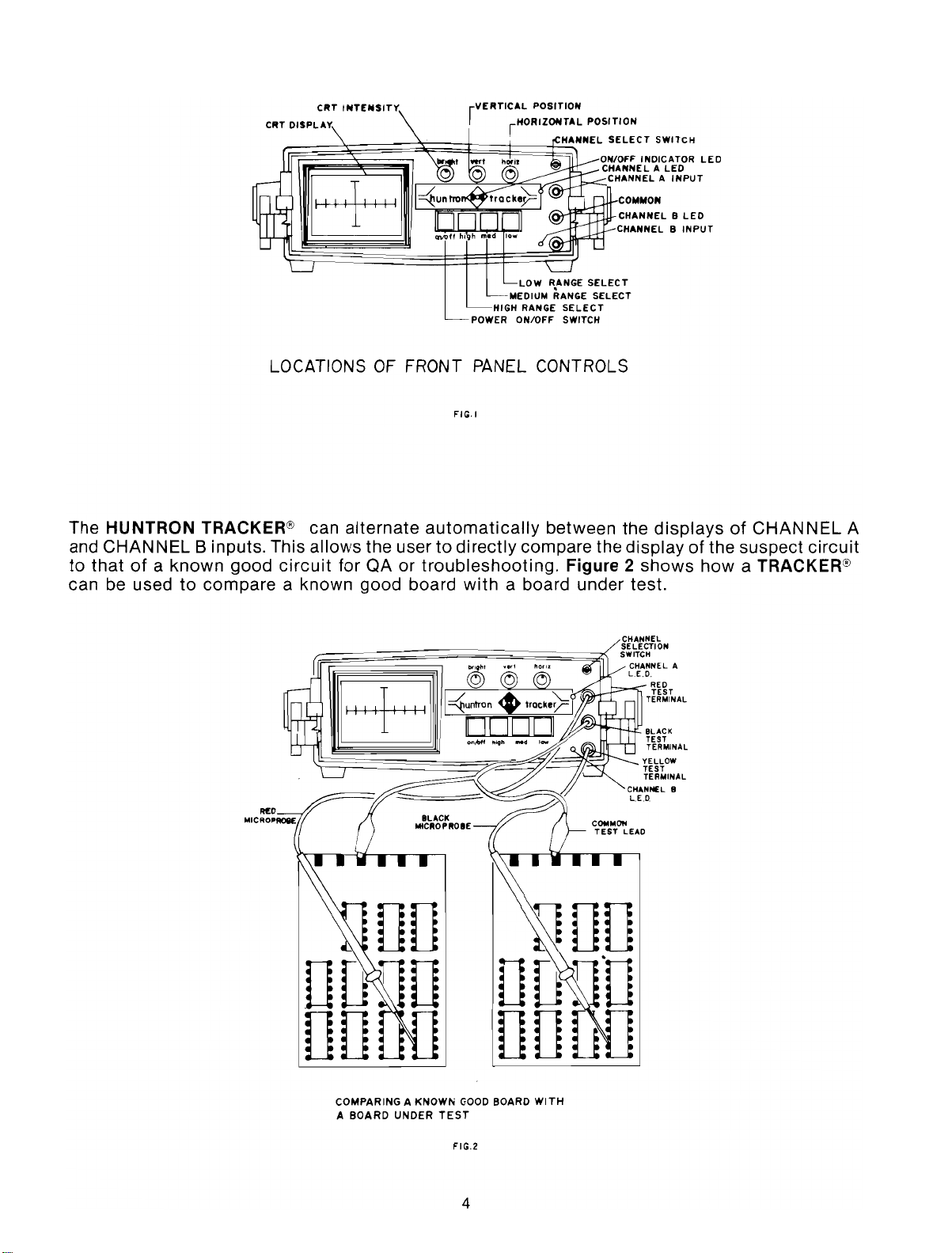
FRONT PANEL CONTROLS
DISPLAY CONTROLS:
BRIGHT
VERT
HORIZ
transistors,
analog
etchings
are
under
that
are
and
as
standard
The MICRO
tipssothat
without
equipment
tested
test.
to
normally
and
digital;
the
is a
withatwo
The
test
test
components
of
resistive values.
tested by the TRACKER®
field
effect
certain
equipment
PROBE™
they
can be usedtocontact
dangerofshorting
common
2).
AND
special
the
leads are
circuit
typesofcapacitors
leads
test
INDICATORS (RefertoFigure
typeofCRT
qualityofcertain
terminal
boardsorother in-circuit
transistors;
with
plug
lead
system
inserted
in a
each TRACKER® is a
into
adjacent
which
Controls
Controls
Controls
display
typesofelectronic
of
power-off
include
bipolar
and
the
front
very
is used
the
intensity
the
vertical
the
horizontal
test
into
and MOS
small
terminals
with
and
signal
leads
the TRACKER®
condition,
conditions
the
following:
integrated
inductors.
set
panel
test
component
and leads.
the TRACKER® in the
1)
of
CRT
position
position
processing
that
are placed
and can be used
even
semiconductor
of
HUNTRON® MICRO
jacks.
display
of
of
instrument
components.
across
front
with
circuits,
MICRO
terminals
Also
CRT
CRT
panel. The
components
PROBES™
and
included
"Compar-
display
display
the
to
test
diodes,
including
small
as
RANGE SELECTOR SWITCH:
Three
HIGH
MED
LOW
CHANNEL
Three
Top
Center
Bottom
(ALTERNATE MODE
ON/OFF SWITCH 2-position
CHANNEL
CHANNEL
ON/OFF INDICATOR LED
RED TERMINAL
YELLOW
BLACK
interlocking
SELECT SWITCH:
position
position
position
position
A LED
BLED
TERMINAL
TERMINAL
switch
selects
selects
selects
pushbutton
that
CHANNEL
ALTERNATE MODE.
CHANNEL
alternates
switches
selects
A.
display
select
Selects
Selects
Selects
the
channel
B.
between
OFF
Indicates
Indicates
Indicates
CHANNEL
CHANNEL
INSTRUMENT
oneofthree ranges characterized below.
displayed.
two
120 V
40VP-P
20 V
P-P
sine
sine
wave
P-P
sine wave
inputs
pushbotton
CHANNELAinput
CHANNELBinput
POWER is ON
A INPUT
B INPUT
at 0.8 Hz
that
COMMON
wave
turns
or
test
signal
test
signal
test
signal
for
Good/Bad comparison.)
the
TRACKER@
is being
is being
OFF
displayed
displayed
ON
or
3
CRT
CRT
DISPLAY
INTENSITY
VERTICAL
POSITION
HORIZONTAL
POSITION
rrn~~~~~~~~~r~;~IF~i~H~ANNEL
--"::i\=!;:=;!!!~"""'l'"...r..J
+
LOCATIONS OF FRONT PANEL CONTROLS
The HUNTRON TRACKER® can
and CHANNEL B inputs. This allows the user
to
thatofa known good
can be used
to
compare a known good board
circuit
alternate
for QA or
SELECT
SWITCH
CO
....
u."'--t"F-T"'T11
lOW
RANGE
MEDIUM RANGE SELECT
HIGH RANGE
POWER ON/OFF SWITCH
FIG.I
automatically
to
directly compare the displayofthe suspect
troubleshooting.
with
a board under test.
SELECT
SELECT
between the
Figure 2
ON
LCHAN
NElBlED
CHANNEL B
INPUT
displaysofCHANNEL
shows
how a TRACKER®
A
circuit
CHANNEL
SELECTION
SWITCH
CHANNEL A
LE.D.
RED
TEST
TERMINAL
EBIIII~Oiiiiif--'//=
BLACK
TEST
TERMINAL
YELLOW
TEST
TERMINAL
CHANNEL B
L.E.D.
DO
IJD~H]
aD
COMPARING A KNOWN
A
BOARD
UNDER
TEST
GOOD
FIG.2
4
BOARD
WITH
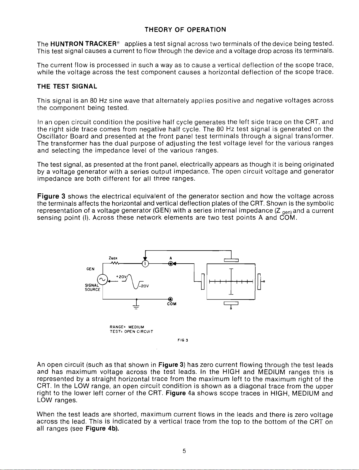
THEORY
OF
OPERATION
The HUNTRON TRACKER® applies a test signal across
two
terminalsofthe device being tested.
This test signal causes a current to flow through the device and a voltage drop across its terminals.
The
current
while
THE
This
the
the
TEST
signal is an
component
In an open
the
right
Oscillator
The
transformer
and
selecting
flow
voltage
SIGNAL
is processed in
across
80
the
Hz sine wave
such
test
component
that
being tested.
circuit
side trace
condition
comes
the
positive
from negative
Board and presented at the
has the dual purposeofadjusting
the
impedance
levelofthe
a way astocause a vertical
causesahorizontal
alternately
half
half
front
various
cycle
applies
generates the
positive
cycle. The 80 Hz
panel
test
the
terminals
test
ranges.
voltage
deflectionofthe
deflection
of
and negative
left
side
trace on the CRT, and
test
signal
is generated on the
throughasignal
level
for
the
scope
the
scope
voltages
transformer.
various
trace,
trace.
across
ranges
The test signal, as presented at the front panel, electrically appears as though it is being originated
by a
voltage
impedance
Figure 3
the terminals
representation
sensing
are
shows
point
generator
both
the
affects
of
(I).
with
a series
different
electrical
for
equivalentofthe
the horizontal and vertical deflection platesofthe
a voltage generator (GEN)
Across
these
network
output
impedance. The open
all three ranges.
generator
with
a series internal impedance
elements
are
two
section
test
points
circuit
and
how
CRT.
A and COM.
voltage
the
and
generator
voltage
across
Shown is the symbolic
(Z
gen) and a current
ZGEN
GEN
+20~
tV
+--
RANGE= MEDIUM
TEST= OPEN CIRCUIT
voltage
straight
that
shown
across
horizontal
An open
and has
circuit
maximum
represented by a
SIGNAL
SOURCE
(such as
CRT. In the LOW range, an open
righttothe
lower
left
cornerofthe CRT. Figure 4a
LOW ranges.
test
When the
across
the lead. This is
all ranges (see
leads are shorted,
indicated
Figure 4b).
A
-20V
COM
flG3
in Figure3)has zero
the
test
leads. In the HIGH and MEDIUM ranges
trace
circuit
maximum
by a vertical
from the
conditionisshown
current
trace
current
maximum
shows
flows
scope
in the leads and there is zero
from the
flowing
lefttothe
as a
diagonal
traces
top
to the
through
maximum
trace
the
test
rightofthe
from
the
leads
this
upper
is
in HIGH, MEDIUM and
voltage
bottomofthe CRT on
5
+
HIGH
+
TEST:
OPENCIRCUIT
FIG.4.
MED
LOW
+
HIGH
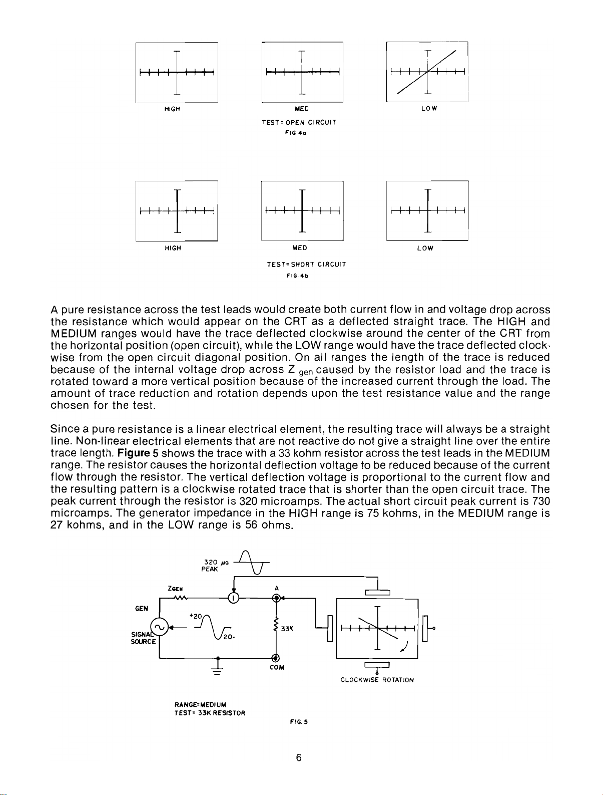
A pure resistance across the test leads would create both current
the
resistance
MEDIUM ranges
the horizontal
wise
from the open
because
rotated
amountoftrace
chosen
Since a pure resistance is a linear electrical element, the resulting trace will alwaysbea
line. Non-linear
trace length.
range. The resistor causes the horizontal
flow
the
peak
microamps.
27 kohms, and in the LOW range is
of
toward
for
through
resulting
current
which
position
the
internal voltage
a more vertical
the
test.
electrical
Figure 5 shows the trace with a
the resistor. The vertical
pattern is a
through
The
would
would
reduction
generator
have the trace
(open circuit),
circuit
the
appear on the CRT as a
diagonal
drop
position
and
rotation
elements
clockwise
resistor
impedance in
is 320
+
MED
TEST:
SHORT CIRCUIT
FIG.4b
deflected
deflected
while
position.
that
rotated trace
56
the
across Z gen caused by the
becauseofthe increased current
depends upon the
are not reactivedonot give a
33
deflection
deflection
microamps.
the
ohms.
clockwise
LOW range
On
all ranges the lengthofthe
kohm resistor across the test leads in the MEDIUM
voltagetobe
voltage is
thatisshorter
The actual
HIGH range is
would
+
LOW
flow
in and voltage drop across
straight
around the
have the
resistor
test
resistance value and the range
reduced becauseofthe current
proportionaltothe
than the open
short
75
kohms, in the MEDIUM range is
trace. The HIGH and
centerofthe CRT from
trace
deflected
trace is reduced
load and the trace is
through
straight
circuit
peak
the
line over the entire
current
circuit
trace. The
current
clock-
load. The
straight
flow
and
is 730
GEN
SIGN
SOlRCE
ZClEN
rv_
RANGE:MEDIUM
TEST'
3201'0
PEAK
.2~
33K
RESISTOR
20-
~
V
A
COM
33K
FIG.5
6
+~
c::r
CLOCKWiSE
ROTATION
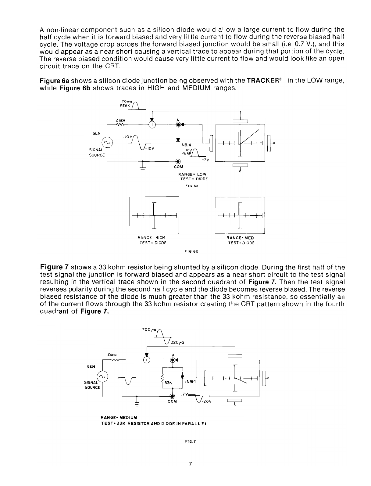
A non-linear
half
cycle
cycle. The
would
appear as a near
component
whenitis forward biased and very
voltage
The reverse biased
circuit
trace
on the CRT.
such
drop
across
short
condition
as a
silicon
diode
the forward biased
causing
would
a vertical
cause very
would
little
allow
currenttoflow
junction
tracetoappear
little
currenttoflow
a large
would
during
currenttoflow
during
the reverse biased
be small (i.e. 0.7
that
portionofthe cycle.
and
would
look
during
the
half
V.),
and
this
like an open
Figure6ashowsasilicon
while
Figure 6b
shows
diode
traces
170~Qf\
PEA~
ZGEN
tIOV(\
- \£0V
junction
being observed
in HIGH and MEDIUM ranges.
A
IN914
IOY(\
COM
RANGE;
TEST;
PEA~
FIG.60
-.7V
LOW
DIODE
+
RANGE;
HIGH
TEST;
DIODE
FIG
6b
with
the TRACKER® in the LOW range,
RANGE-MED
TEST;
DIODE
Figure7showsa33
test
signal
resulting
reverses
biased
of
the
the
junctionisforward
in the
polarity
vertical
during the second
resistanceofthe
current
flows
quadrantofFigure
kohm
through
7.
ZGEN
RANGE-
TEST-33K
resistor
being
biased and appears as a near
trace
showninthe
half
diodeismuch
the
33 kohm
7001'0(\
~20ro.
MEDIUM
RESISTOR AND
shunted
second
cycle
and the
greater
than the
resistor
A
COM
IN914
.7V==t/
V-20V
FIG.7
33K
DIODEINPARALLEL
by a
silicon
quadrant
diode
creating
"
diode. During the
short
of
Figure7.Then the
circuit
first
to the
ha.lfofthe
test
signal
test
signal
becomes reverse biased. The reverse
33
kohm resistance, so
the CRT
"~-=::+-+---t--II
pattern
I
~
shown
essentially
in the
fourth
all
cr
7
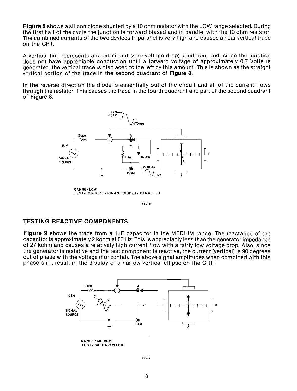
Figure 8 shows a silicon diode shunted by a
first
the
halfofthe cycle the
The combined currents
on the CRT.
of
junction
the
is forward biased and in parallel
two
devices in parallel is very high and causes a near vertical trace
10
ohm resistor with the LOW range selected. During
with
the10ohm resistor.
A vertical line represents a short
does not have appreciable
conduction
circuit
generated, the vertical trace is displaced
vertical portionofthe trace in the second quadrant
In the reverse
direction
the
diodeisessentially
(zero voltage drop)
until
a forward voltage
to
the
leftbythis
of
Figure
outofthe
condition,
of
and, since the
approximately
0.7
amount. This is shown as the
8.
circuit
and allofthe current
junction
Volts
straight
flows
through the resistor. This causes the trace in the fourth quadrant and partofthe second quadrant
of
Figure
8.
ZIIlEN
RANGE-
TEST-IO,/\,
LOW
RESISTOR
170mQ
PEAl<
~!\
--U70mQ
AND
DIODEINPARALLEL
10.1\.
COM
IN9/4
is
FIG.8
TESTING REACTIVE COMPONENTS
Figure 9
shows
capacitor is approximately 2 kohm at
of27kohm and causes a relatively high current
the generator is resistive and the
outofphase with the voltage (horizontal). The above signal
phase
shift
the trace from a 1uF
result in the
displayofa narrow vertical ellipse on the CRT.
ZeEN
RANGE-
TEST-
test
'47-
MEDIUM
luF
CAPACITOR
capacitor
80
Hz.
This is appreciably less than the generator impedance
component
A
COM
in the MEDIUM range. The reactanceofthe
flow
with
is reactive, the current (vertical) is 90 degrees
luF
a fairly low voltage drop. Also, since
amplitudes
when combined with
this
FIG.9
8
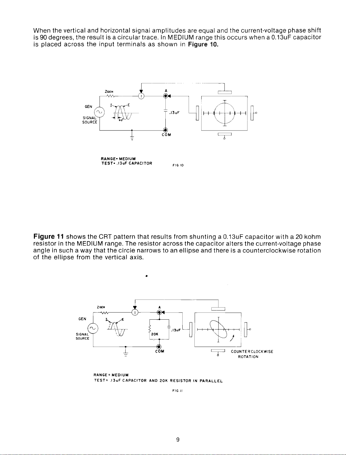
When the vertical and horizontal
is90degrees, the result is a
is placed
across
the
input
circular
terminals
ZGEN
signal
amplitudes
trace.InMEDIUM range
as
shown
in Figure 10.
are equal and the current-voltage phase
this
occurs
when a 0.13uF
capacitor
shift
Figure
resistor
angle
of
the
11
shows
the
RANGE-
TEST-
CRT
MEDIUM
.13uF
pattern
in the MEDIUM range. The
in such a way
ellipse
that
from the
ZGEN
the
circle
vertical
I~,
I "
\ I
"'
CAPACITOR
that
resistor
narrowstoan
axis
E
.
results
across
A
COM
FIG
from
.13uF
10
shunting
the
ellipse
a 0.13uF
capacitor
alters the current-voltage phase
and there is a
capacitor
counterclockwise
+I~
L--
~
J
COUNTERCLOCKWISE
ROTATION
with
a 20 kohm
rotation
RANGE:
TEST:
MEDIUM
.13uF
CAPACITOR
AND
20K
RESISTORINPARALLEL
FIG.II
9

CIRCUIT DESCRIPTION
SIGNAL SECTION:
Figure
is shown
12
is a basic
with
circuit
representationofthe signal sectionofthe TRACKER® . The
a test diode in place.
6.8
RI
PR I SEC
circuit
TI
{\
V
FIG,12
VERT
R8
-
-
HORIZ
TEST
DIODE
-
-
During the half cycle portion when the horizontal sideofthe secondary is negative, the test diode
that
very
little
is reverse biased so
R8.
The vertical end of the secondary is very close to ground potential becauseofR8,
current
flows
through the
transformer
secondary and resistor
and a very
small voltage appears on the vertical lead. •
of
Since the impedance across the horizontal side
appearing on the vertical side, most
half
During the next
approximately
of
side
that
the secondary. The voltage that appears acrossR8is a direct representationofthe current
flows
through the test diode.
.7
cycle the horizontal side will go positive and the test diode
Volt. Also current will
of
the secondary voltage
flow
through
the secondary is very high relative to that
will
appear on the horizontal side.
will
clamp
R8
creating a large voltage at the vertical
at
10
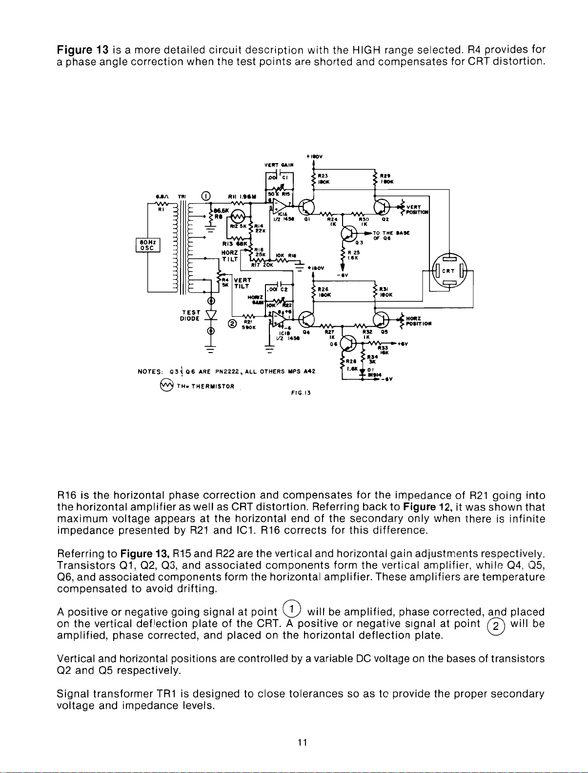
Figure
a phase
13
is a more
angle
detailed
correction
circuit
when the
description
test
points
are
with
the HIGH range selected.
shorted
and
compensates
for
R4
provides
CRT
for
distortion.
80Hz
osc
NOTES:
RI
e
Q 3~Q 6
TH.
ARE
PN2222,
THERMISTOR
ALL
VEIIT
OTHERS
84IN
MPS
FIG.13
+IeoV
A42
R23
1101(
RZ4
IK
-IV
L--___4__-&V
TO
Of'
R31
1I0K
l+-..-JvVv--+&V
R2I
I.U
R34
3K
01
IN.H
R53
VEIIT
POSITION
QZ
THE
lASE
01
HOltZ
~1T10ll
IIll
R16
is the horizontal phase
the
horizontal
maximum
impedance
amplifier
voltage
appears at the
presented by
ReferringtoFigure 13,
Transistors
06,
and
compensated
A
positiveornegative
on the vertical
amplified,
01,02,03,
associated
components
to
avoid
deflection
phase corrected, and placed on the
R15
going
correction
as well as CRT
horizontal
R21
and IC1.
and
R22
are the vertical and horizontal gain
and
associated
form the
drifting.
signalatpoint
plateofthe CRT. A
and
compensates
distortion.
endofthe
R16
corrects
components
horizontal
CD
positive
Referring
for
form
amplifier.
will
be
amplified,
or
horizontal
Vertical and horizontal positions are controlled by a variable
02
and
05
respectively.
Signal
voltage
transformer
and
impedance
TR1isdesignedtoclose
levels.
tolerances
11
for
the
impedanceofR21
backtoFigure
secondary
this
difference.
only
the vertical
These
amplifiers
phase
negative
signal
deflection
DC
voltage on the basesoftransistors
so astoprovide the
12,itwas
when there is
adjustments
amplifier,
respectively.
while
are
temperature
corrected, and placed
at
point
plate.
proper
going
shown
into
that
infinite
04,
0
will
secondary
05,
be
 Loading...