

hunix HY5DU121622CTP User Manual

查询HY5DU121622CTP-4供应商
Rev. 0.3 / Apr. 2005 2
1HY5DU121622CTP
Revision History
Revision No. History Draft Date Remark
0.1 Initial Graphics Version Release Jan. 2005
0.2 Lead free Support & DC parameter change Apr. 2005
0.3 IDD Value change Apr. 2005
Rev. 0.3 / Apr. 2005 3
1HY5DU121622CTP
Preliminary
DESCRIPTION
The HY5DU121622CTP is a 536,870,912-bit CMOS Double Data Rate(DDR) Synchronous DRAM, ideally suited for the
main memory applications which requires large memory density and high bandwidth.
This Hynix 512Mb DDR SDRAMs offer fully synchronous operations referenced to both rising and falling edges of the
clock. While all addresses and control inputs are latched on the rising edges of the CK (falling edges of the /CK), Data,
Data strobes and Write data masks inputs are sampled on both rising and falling edges of it. The data paths are internally pipelined and 2-bit prefetched to achiev e v e ry high b andwidth. All input and output voltage levels are compatible
with SSTL_2.
FEATURES
•VDD, VDDQ = 2.5V +/- 0.1V
• All inputs and outputs are compatible with SSTL_2
interface
• Fully differential clock inputs (CK, /CK) operation
• Double data rate interface
• Source synchronous - data transaction aligned to
bidirectional data strobe (DQS)
• x16 device has two bytewide data strobes (UDQS,
LDQS) per each x8 I/O
• Data outputs on DQS edges when read (edged DQ)
Data inputs on DQS centers when write (centered
DQ)
• On chip DLL align DQ and DQS transition with CK
transition
• DM mask write data-in at the both rising and falling
edges of the data strobe
• All addresses and control inputs except data, data
strobes and data masks latched on the rising edges
of the clock
• Programmable /CAS latency 3 supported
• Programmable burst length 2 / 4 / 8 with both
sequential and interleave mode
• Internal four bank operations with single pulsed
/RAS
• Auto refresh and self refresh supported
• tRAS lock out function supported
• 8192 refresh cycles / 64ms
• JEDEC standard 400mil 66pin TSOP-II with 0.65mm
pin pitch
• Full and Half strength driver option controlled by
EMRS
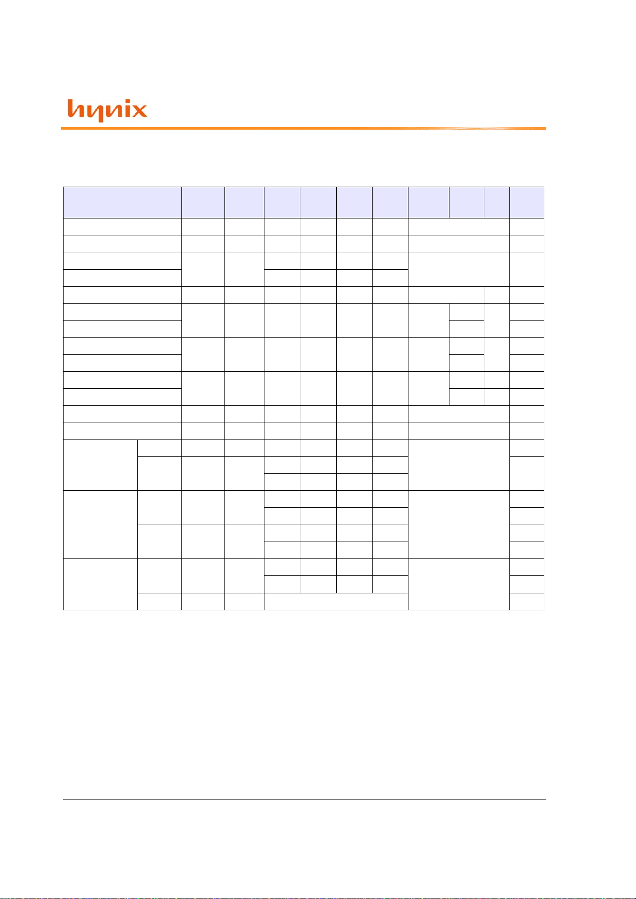
ORDERING INFORMATION
Note) Hynix supports Pb free parts for each speed grade with same specification, except Lead free material.
We'll add "P" character after "T" for Lead free product.
For example, the part number of 200Mhz Lead free product is HY5DU121622CTP-5.
Part No. Power Supply
Clock
Frequency
Max Data Rate Interface Package
HY5DU121622CTP - 4
VDD/
VDDQ=2.5V
250Mhz 500Mbps/pin
SSTL_2
400mil
66pin
TSOP-II
HY5DU121622CTP - 5 200Mhz 400Mbps/pin
HY5DU121622CTP - 6 166Mhz 333Mbps/pin
Rev. 0.3 / Apr. 2005 4
1HY5DU121622CTP
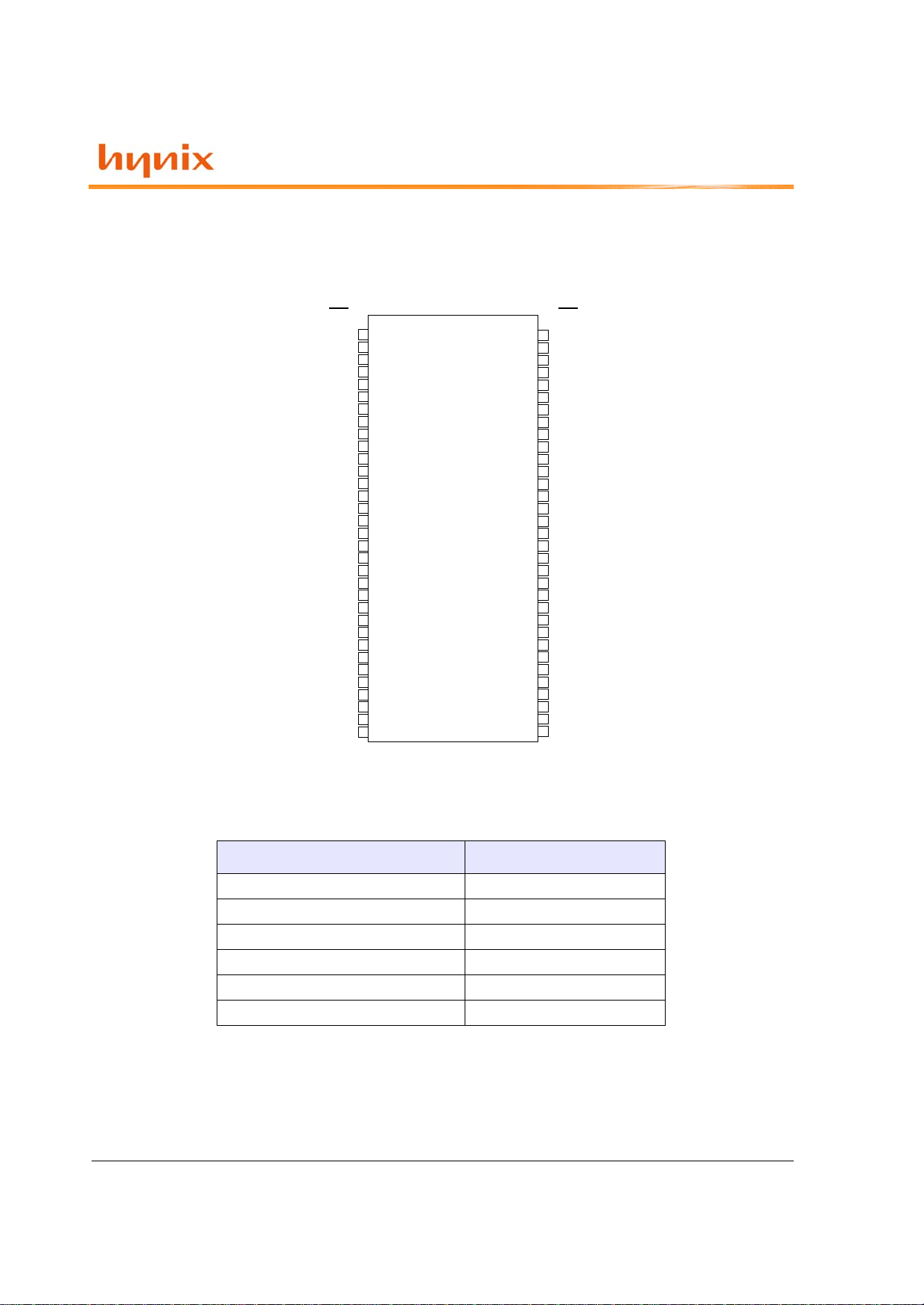
PIN CONFIGURATION
66
65
64
63
62
61
60
59
58
57
56
55
54
53
52
51
50
49
48
47
46
45
44
43
42
41
40
39
38
37
36
35
34
1
2
3
4
5
6
7
8
9
10
11
12
13
14
15
16
17
18
19
20
21
22
23
24
25
26
27
28
29
30
31
32
33
VDD
DQ0
VDDQ
DQ1
DQ2
VSSQ
DQ3
DQ4
VDDQ
DQ5
DQ6
VSSQ
DQ7
NC
VDDQ
LDQS
NC
VDD
NC
LDM
/WE
/CAS
/RAS
/CS
NC
BA0
BA1
A10/AP
A0
A1
A2
A3
VDD
VSS
DQ15
VSSQ
DQ14
DQ13
VDDQ
DQ12
DQ11
VSSQ
DQ10
DQ9
VDDQ
DQ8
NC
VSSQ
UDQS
NC
VREF
VSS
UDM
/CK
CK
CKE
NC
A12
A11
A9
A8
A7
A6
A5
A4
VSS
x16x16
400mil X 875mil
66pin TSOP -II
0.65mm pin pitch
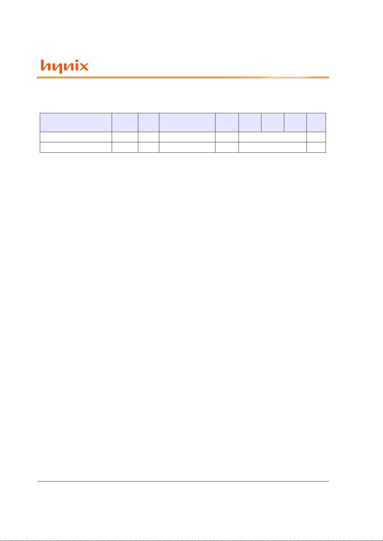
ROW AND COLUMN ADDRESS TABLE
ITEMS 32Mx16
Organization 8M x 16 x 4banks
Row Address A0 - A12
Column Address A0-A9
Bank Address BA0, BA1
Auto Precharge Flag A10
Refresh 8K

Rev. 0.3 / Apr. 2005 5
1HY5DU121622CTP
PIN DESCRIPTION
PIN TYPE DESCRIPTION
CK, /CK Input
Clock: CK and /CK are differential clock inputs. All address and control input signals are
sampled on the crossing of the positive edge of CK and negative edge of /CK. Output
(read) data is referenced to the crossings of CK and /CK (both directions of crossing).
CKE Input
Clock Enable: CKE HIGH activates, and CKE LOW deactivates internal clock signals, and
device input buffers and output drivers. Taking CKE LOW provides PRECHARGE POWER
DOWN and SELF REFRESH operation (all banks idle), or ACTIVE POWER DOWN (row
ACTIVE in any bank). CKE is synchronous for POWER DOWN entry and exit, and for SELF
REFRESH entry . CKE is asynchronous f or SELF REFRESH exit, and f or out put disable. CKE
must be maintained high throughout READ and WRITE accesses. Input buffers, excluding
CK, /CK and CKE are disabled during POWER DOWN. Input buffers, excluding CKE are
disabled during SELF REFRESH. CKE is an SSTL_2 input, but will detect an LVCMOS LOW
level after Vdd is applied.
/CS Input
Chip Select : Enables or disables all inputs except CK, /CK, CKE, DQS and DM. All commands are masked when CS is registered high. CS provides for external bank selection on
systems with multiple banks. CS is considered pa rt of the command code.
BA0, BA1 Input
Bank Address Inputs: BA0 and BA1 define to which bank an ACTIVE, R ead, W rite or PRECHARGE command is being applied.
A0 ~ A12 Input
Address Inputs: Provide the row ad dress f or ACTIVE co mmands, and the colu mn address
and AUTO PRECHARGE bit for READ/WRITE co mmands, to s elect one loc ati on out of th e
memory array in the respective bank. A10 is sampled during a precharge command to
determine whether the PRECHARGE applies to one bank (A10 LOW) or all banks (A10
HIGH). If only one bank is to be precharged, the bank is selected by BA0, BA1. The
address inputs also provide the op code during a MODE REGISTER SET command. BA0
and BA1 define which mode register is loaded durin g the MODE REGISTER SET command
(MRS or EMRS).
/RAS, /CAS, /WE Input
Command Inputs: /RAS, /CAS and /WE (along with /CS) define the command being
entered.
DM
(LDM,UDM)
Input
Input Data Mask: DM is an input mask signal for write data. Input data is masked when
DM is sampled HIGH along with that input data during a WRITE access. DM i s sam pled
on both edges of DQS. Alth ough D M pin s ar e input only, the DM loading matches the DQ
and DQS loading. For the x16, LDM corresponds to the data on DQ0-Q7; UDM corresponds to the data on DQ8-Q15.
DQS
(LDQS,UDQS)
I/O
Data Strobe: Output with read data, input with write data. Edge aligned with read data,
centered in write data. Used to capture write data. For the x16, LDQS corresponds to the
data on DQ0-Q7; UDQS corresponds to the data on DQ8-Q15.
DQ I/O Data input / output pin : Data bus
V
DD/VSS Supply Power supply for internal circuits and input buffers.
V
DDQ/VSSQ Supply Power supply for output buffers for noise immunity.
V
REF Supply Reference voltage for inputs for SSTL interface.
NC NC No connection.
Rev. 0.3 / Apr. 2005 6
1HY5DU121622CTP
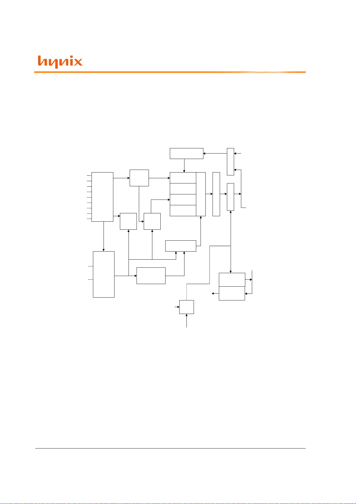
Command
Decoder
CLK
/CLK
CKE
/CS
/RAS
/CAS
/WE
LDM
Address
Buffer
A0~A12
Bank
Control
8Mx16/Bank0
Column Decoder
Column A ddress
Counter
Sense AMP
2-bit Prefetch Unit
8Mx16/Bank1
8Mx16/Bank2
8Mx16/Bank3
Mode
Register
Row
Decoder
Input Buffer
Output Buffer
DLL
Block
Mode
Register
Data Strobe
Transmitter
Data Strobe
Receiver
LDQS, UD Q S
CLK
/CLK
LDQS
UDQS
Write Data Register
2-bit Prefetch Unit
DS
DQ[0:15]
32 16
16
32
CLK_DLL
BA0, BA1
UDM
FUNCTIONAL BLOCK DIAGRAM (32Mx16)
4Banks x 8Mbit x 16 I/O Double Data Rate Synchronous DRAM
Rev. 0.3 / Apr. 2005 7
1HY5DU121622CTP
SIMPLIFIED COMMAND TRUTH TABLE
Command CKEn-1 CKEn CS RAS CAS WE ADDR
A10/
AP
BA Note
Extended Mode Register SetH XLLLL OP code 1,2
Mode Register Set H XLLLL OP code 1,2
Device Deselect
HX
HXXX
X1
No Operation L H H H
Bank Active H X L L H H RA V 1
Read
HXLHLHCA
L
V
1
Read with Autoprecharge H1,3
Write
HXLHLLCA
L
V
1
Write with Autoprecharge H1,4
Precharge All Banks
HXLLHLX
HX1,5
Precharge selected Bank LV1
Read Burst Stop H X L H H L X 1
Auto Refresh H HLLLH X 1
Self Refresh
EntryH LLLLH
X
1
Exit L H
HXXX
1
LHHH
Precharge Power
Down Mode
Entry H L
HXXX
X
1
LHHH 1
Exit L H
HXXX 1
LHHH 1
Active Power
Down Mode
Entry H L
HXXX
X
1
LVVV 1
Exit L H X 1
Note :
1. LDM/UDM states are Don’t Care. Refer to below Write Mask Truth Table.
2. OP Code(Operand Code) consists of A0~A12 and BA0~BA1 used for Mode Register setting duing Extended MRS or MRS.
Before entering Mode Register Set mode, all banks must be in a precharge state and MRS command can be issued after tRP
period from Prechagre command.
3. If a Read with Autoprecharge command is detected by memory component in CK(n), then there will be no command presented
to activated bank until CK(n+BL/2+tRP).
4. If a Write with Autoprecharge command is detected by memory component in CK(n), then there will be no command presented
to activated bank until CK(n+BL/2+1+tDPL+tRP). Last Data-In to Prechage delay(tDPL) which is also called Write Recovery Time
(tWR) is needed to guarantee that the last data has been completely written.
5. If A10/AP is High when Precharge command being issued, BA0/BA1 are ignored and all banks are selected to be
precharged.
( H=Logic High Level, L=Logic Low Level, X=Don’t Care, V=Valid Data Input, OP Code=Operand Code, NOP=No Operation )
Rev. 0.3 / Apr. 2005 8
1HY5DU121622CTP
WRITE MASK TRUTH TABLE
Function CKEn-1 CKEn
/CS, /RAS,
/CAS, /WE
DM
ADDR
A10/
AP
BA Note
Data Write H X X L X 1
Data-In Mask H X X H X 1
Note :
1. Write Mask command masks burst write data with reference to LDQS/UDQS(Data Strobes) and it is not related
with read data. In case of x16 data I/O, LDM and UDM control lower byte(DQ0~7) and Upper byte(DQ8~15)
respectively.
Rev. 0.3 / Apr. 2005 9
1HY5DU121622CTP
OPERATION COMMAND TRUTH TABLE-I
Current
State
/CS /RAS /CAS /WE Address Command Action
IDLE
HXXX X DSEL
NOP or power down
3
LHHH X NOP
NOP or power down
3
LHHL X BST
ILLEGAL
4
L H L H BA, CA, AP READ/READAP
ILLEGAL
4
L H L L BA, CA, AP WRITE/WRITEAP
ILLEGAL
4
L L H H BA, RA ACT Row Activation
LLHLBA, AP PRE/PALL NOP
LLLH X AREF/SREF
Auto Refresh or Self Refresh
5
L L L L OPCODE MRS Mode Register Set
ROW
ACTIVE
HXXX X DSEL NOP
LHHH X NOP NOP
LHHL X BST
ILLEGAL
4
L H L H BA, CA, AP READ/READAP
Begin read : optional AP
6
L H L L BA, CA, AP WRITE/WRITEAP
Begin write : optional AP
6
LLHHBA, RA ACT
ILLEGAL
4
LLHLBA, AP PRE/PALL
Precharge
7
LLLH X AREF/SREF
ILLEGAL
11
LLLLOPCODE MRS
ILLEGAL
11
READ
H X X X X DSEL Continue burst to end
L H H H X NOP Continue burst to end
L H H L X BST Terminate burst
L H L H BA, CA, AP READ/READAP
Term burst, new read:optional AP
8
L H L L BA, CA, AP WRITE/WRITEAP ILLEGAL
LLHHBA, RA ACT
ILLEGAL
4
L L H L BA, AP PRE/PALL Term burst, precharge
LLLH X AREF/SREF
ILLEGAL
11
LLLLOPCODE MRS
ILLEGAL
11
WRITE
H X X X X DSEL Continue burst to end
L H H H X NOP Continue burst to end
LHHL X BST
ILLEGAL
4
L H L H BA, CA, AP READ/READAP
Term burst, new read:optional AP
8
L H L L BA, CA, AP WRITE/WRITEAP Term burst, new write:optional AP
 Loading...