

Page 1
User’s Manual and Data
Sheet
PulsON® 412
DRAFT Final Version available Jan 31, 2013
Nov 2012
TIME DOMAIN
Cummings Research Park
4955 Corporate Drive Suite 101
Huntsville, AL 35805 USA
http://www.timedomain.com
Tel: +1 256.922.9229
+1 888.826.8378
Fax: +1.256.922.0387
®
Page 2

2 P412 User’s Manual & Data Sheet
Copyright
All rights reserved. Time Domain® 2001-2012. All rights reserved.
Trademarks
Time Domain®, PulsON®, and “PulsON Triangle” logo are registered trademarks of Time Domain. Microsoft® and
Windows XP®, Windows Vista®, and Windows 7® are registered trademarks of Microsoft Corporation. Any trademarks,
trade names, service marks or service names owned or registered by any other company and used in this manual are the
property of its respective company.
Rights
Rights to use this documentation are set forth in the PulsON Products Terms and Conditions of Sale.
Page 3

P412 User’s Manual & Data Sheet 3
Overview
This document is the user’s manual and data sheet for the Time Domain PulsON 412 (“P412”) Ultra
Wideband (UWB) ranging radio transceiver. The document is divided into the following sections.
Section 1 Summary and Theory of Operation
Section 2 Using a P412 as a Ranging Radio
Section 3 Hardware Block Diagram
Section 4 Interfaces
Section 5 Mechanical
Section 6 Performance Specs
Section 7 Broadspec Antenna
Section 8 FCC Compliance
Section 9 Export Restrictions
1 Summary and Theory of Operation
The P412 is an Ultra Wideband (UWB) radio transceiver that provides the following functions:
• It accurately and reliably measures the distance between two P412s and provides these
measurements at a high update rate.
• It supports two different range measurement techniques (Two-Way Time-of-Flight and
Coarse Range Estimation).
• It communicates data between two or more P412s.
Time Domain’s PulsON P412 is a ruggedized, industrial UWB platform. The most obvious and
important characteristics of the device relative to industrial operation are listed below:
• The electrical interface to the unit through USB, Serial or CAN
• All components are rated for industrial temperature (-40C to +85C)
• Fan is not required for cooling.
• For best performance, the user must provide a heat sink to insure that the unit does not
overheat
• The board is provided with nine large (#6) mounting holes that insure that the unit will
survive and operate in most high vibration environments
• RF filtering provides superior operation in the presence of 2.4GHz and 5.8GHz
• The UWB emissions have been tested and comply with FCC 15.519 which is the most
stringent of the FCC UWB limits
• The digital emissions have been tested and comply with the FCC 15.109(b) (“Class A digital
device”) which limits use of the P412 to commercial and industrial uses only
The P412 is an Ultra Wideband radio that coherently transmits and receives trains of individual RF
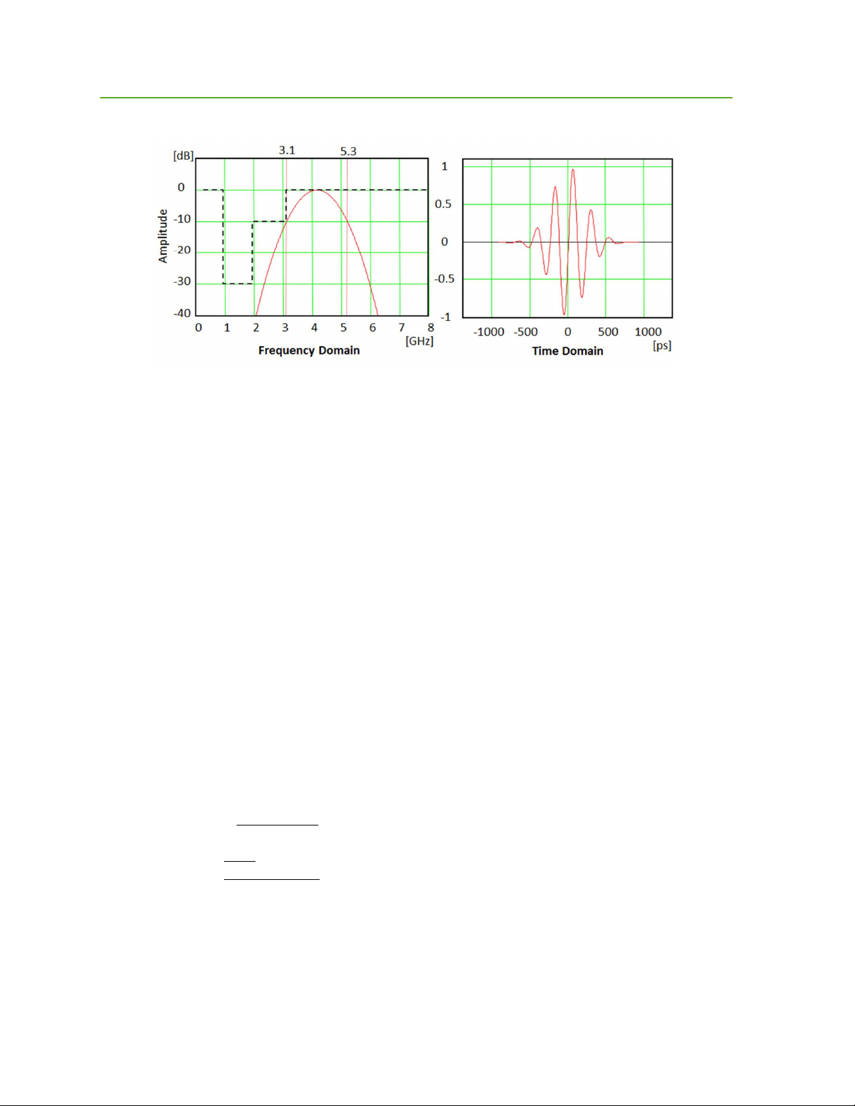
pulses at a nominal rate of 10 MHz. Figure 1 provides a notional example of a typical UWB pulse
in both the time and frequency domain. Pulses are transmitted as coded trains of pulses. Coding is
accomplished either by pseudo-randomly shifting the pulse phase or inter pulse transmission time.
By transmitting and receiving pulses coherently, the P412 can integrate multiple pulses and thereby
increase the received signal to noise ratio. Integration can therefore be used to increase robustness
and or operational range.
Page 4
4 P412 User’s Manual & Data Sheet
Figure 1: Notional UWB pulse in both time and frequency domain.
The P412 measures distance using a technique called Two Way Time of Flight. In this approach the
radio requesting the range measurement (the Requestor) will transmit a packet of pulses that will be
received by one or more units (the Responders). The responder will then measure the leading edge
of the waveform relative to the radio lock spot and transmit this information in a return (or
responding) packet. The Requestor will then measure the difference in phase between the transmitted
and received PN code and compensate this phase measurement by the leading edge measurement.
Dividing the result by two and multiplying by the speed of light yields a measurement of the distance
between the Requestor and Responder.
The user controls and monitors the P412 through a straight forward Application Programming
Interface (API) over USB, Serial or CAN connections. USB driver support is provided for Vista 32,
Vista 64, Win7 32 and Win7 64 operating systems. The API provides all the commands and
capabilities required by a user to design a network tailored for operating multiple P412s as ranging
radios. For details on the API see the following document:
• Ranging and Communications Module API Specification
For details on the USB and serial interfaces refer to
• USB and Serial Interfaces
To assist the user in demonstrating the performance of the P412 as a ranging radio, Time Domain also
provides a PC based Graphical User Interface (GUI). These GUI allows the user to exercise all of the
API commands and offers the following capabilities:
• They provide programmers with a visual example of a host application which interfaces to
the P412 through the API.
• They allow users to evaluate ranging and communications performance.
• They allow system analysts to visualize, collect and log raw ranging data such that it is
possible to develop algorithms/strategies tailored to a given application
Time Domain also provides sample C and Matlab for demonstrating the interface and performance of
the hardware.
For details on these GUIs refer to the following document:
• Ranging and Communications Module Reconfiguration and Evaluation Tool (RCM –
RET) User Guide
Page 5
P412 User’s Manual & Data Sheet 5
Additional information including all of the documents referenced in this section can be found on the
web at www.timedomain.com. This includes: the API, software manuals, applications notes, white
papers, examples, published papers, sample C code, sample Matlab, etc.
2 Using a P412 as a Ranging Radio
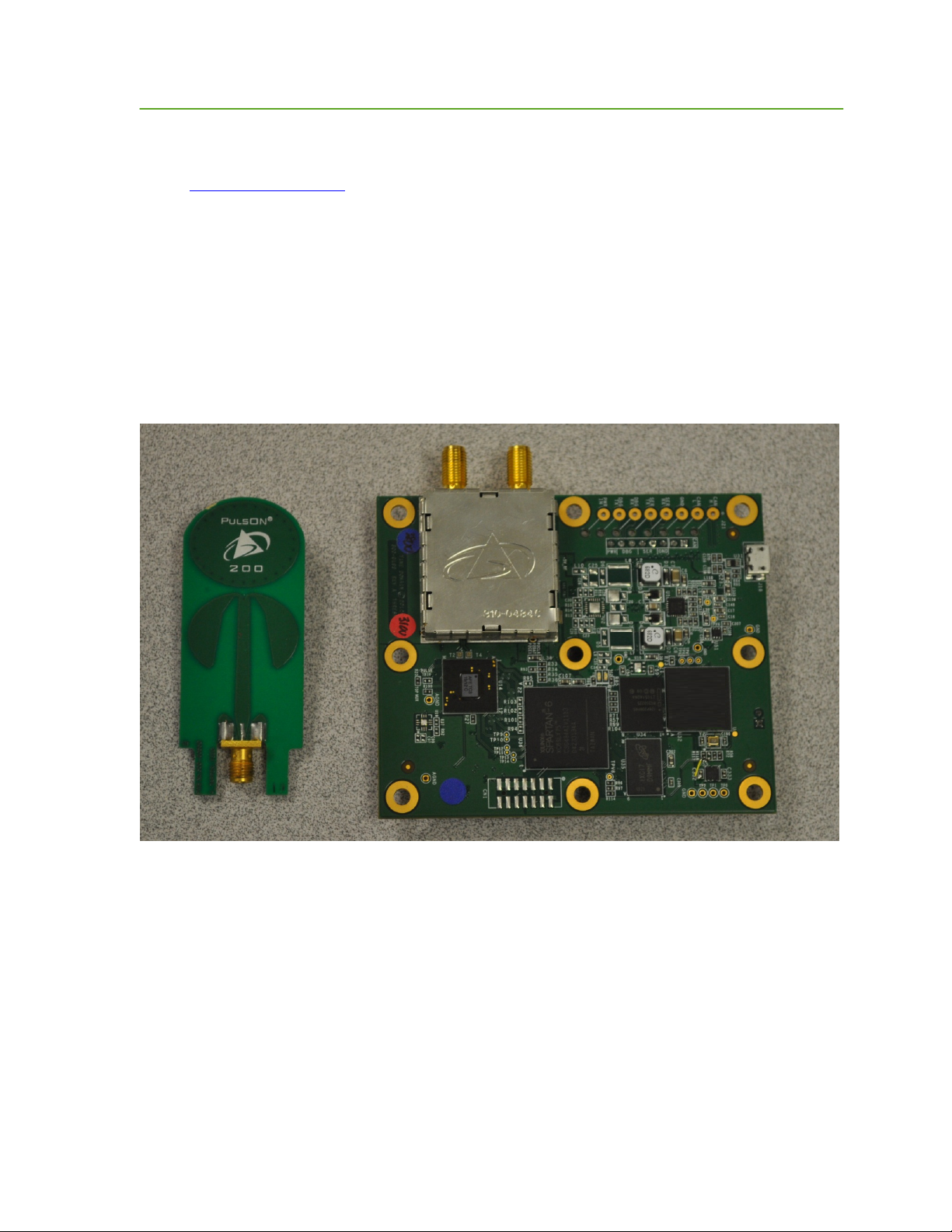
The P412, shown in Figure 2, is a small, low power and affordable device which provides accurate,
high rate range measurements and has superior operational performance when compared to
conventional RFID/RTLS devices. The device is intended for use as an OEM module. When used as
a ranging radio it is typically referred to as a P412 RCM.
Fig. 2: P412 RCM with Broadspec antenna
Time Domain does not provide a standard network as part of the API. Instead, Time Domain is
focused on providing a robust platform and a full featured, flexible interface. This focus includes all
aspects of the physical and link layers as well as a few additional mechanisms to support
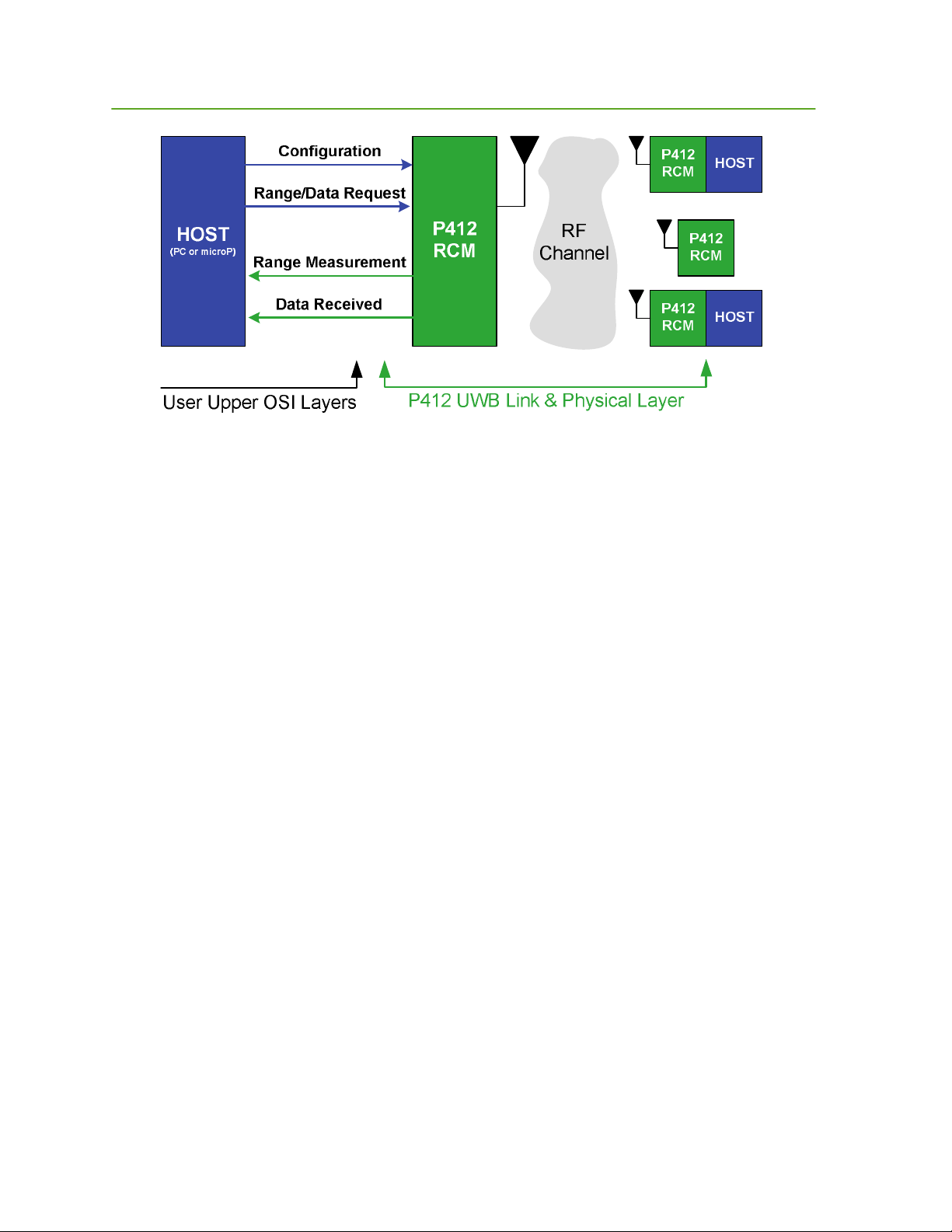
implementation of a wide variety of network architectures. A block diagram showing operation of a
ranging system is provided in Figure 3.
Page 6
6 P412 User’s Manual & Data Sheet
Fig. 3: Illustration of the interface with a system of P412 RCMs
Key Features of the P412 RCM
• Excellent performance in high multipath and high clutter environments
• Coherent signal processing extends operating range
• Direct sequential pulse sampling allows measurement of received waveform (resultant
waveform is available to the user for ranging optimization)
• Two-Way Time-of-Flight (TW-TOF) ranging technique provides highly precise range
measurements with industry-leading update rate
• Coarse Range Estimation (CRE) technique estimates the range from a transmitting unit by
using the received leading edge signal strength and periodically recalibrating the estimate
based on infrequent TW-TOF range measurements
• UWB chipset enables low cost, small size, and low power operation
• UWB waveform and pseudo random encoding ensures noise-like transmissions with a very
small RF footprint
• RF emissions compliant with FCC limits
• Each unit is a full transceiver
• Single 3.1”x 3.7” (7.9 x 9.4 cm) board
• USB or Serial interfaces or CAN
• Several sleep modes allow user to reduce power consumption
Typical Applications of the P412 RCM
• Peer-to-peer ranging with moderate-rate wireless communications
• GPS augmentation for multipath resistance
• Inertial augmentation for drift removal
• Robotics navigation and tracking, precision formation
• Autonomous vehicle convoys
• First responder tracking and man-down locator
• Asset tracking, especially in applications that preclude the use of fixed infrastructure or
involving moving frames of reference
• Distributed sensor automatic survey and dynamic mapping with fused data communications
• Wireless channel impulse response (CIR) measurements
Page 7
P412 User’s Manual & Data Sheet 7
• Wireless noise-like / covert data communications
3 Hardware Block Diagram
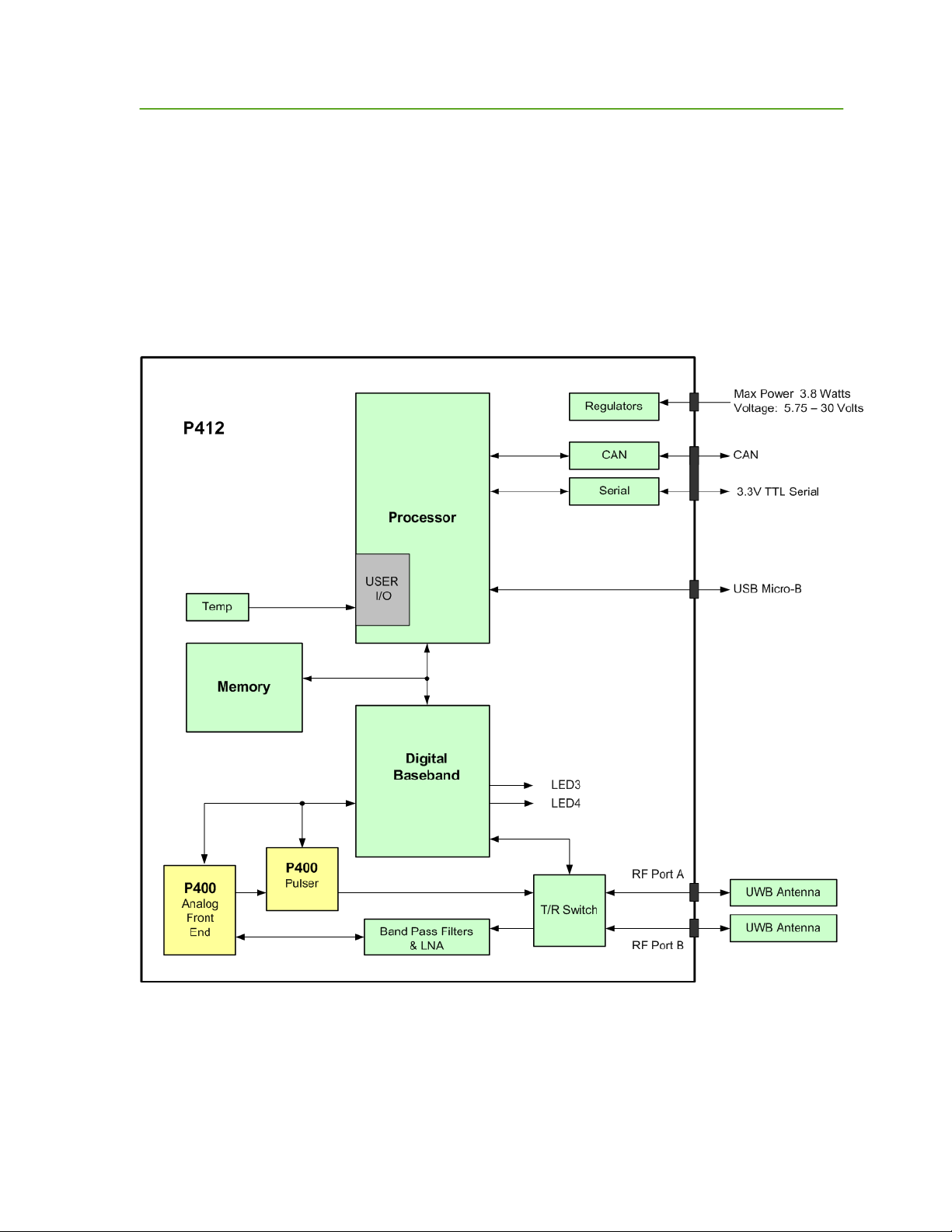
This section provides and discusses at a high level the P412 functional hardware block diagram, as
shown in Figure 4. Additional detail on the various interfaces is provided in Section 4.
Fig. 4: P412 hardware functional block diagram
To power the board, the user must supply a maximum of 3.8 Watts at any voltage between 5.75-30V.
This can be accomplished either with the provided power supply or from a battery. Indicating lights
provide operating status information.
Page 8

8 P412 User’s Manual & Data Sheet
The user can interface to the P412 through either USB (standard USB Micro B connector), Serial
connection, or CAN. In addition, the user can request the P412 to report the board temperature.
The physical interface to the P412 is through a pigtail (not provided). Provisions for soldering the
pigtail to the board are provided. Each of the pigtail holes is also provided with a strain relief hole. If
desirable, the user can lace each of the pigtail wires through the strain relief hole before soldering at
the pad. Details are provided in Section 4.
The processor controls the UWB front end through a Digital Baseband FPGA interface. More
specifically, the FPGA configures the Time Doman P412 Pulser chip (UWB transmitter) and P412
Analog Front End (AFE) chip (UWB receiver), provides timing signals and out-going data, receives
incoming data and controls the position of the transmit/receive (T/R) switch.
There are three RF sections:
• The Pulser chip transmits a train of UWB pulses at the maximum allowable FCC transmit
levels. The Pulser chip is also provided with a variable attenuator that allows the user to
reduce the transmit power to as little as 19 dB below the FCC limit.
• Receive chain consists of gain stages and band pass filter.
• T/R switch supports two configurations: Transmit/Receive on Port A and Transmit on A,
Receive on B.
Page 9
P412 User’s Manual & Data Sheet 9
4 Interfaces
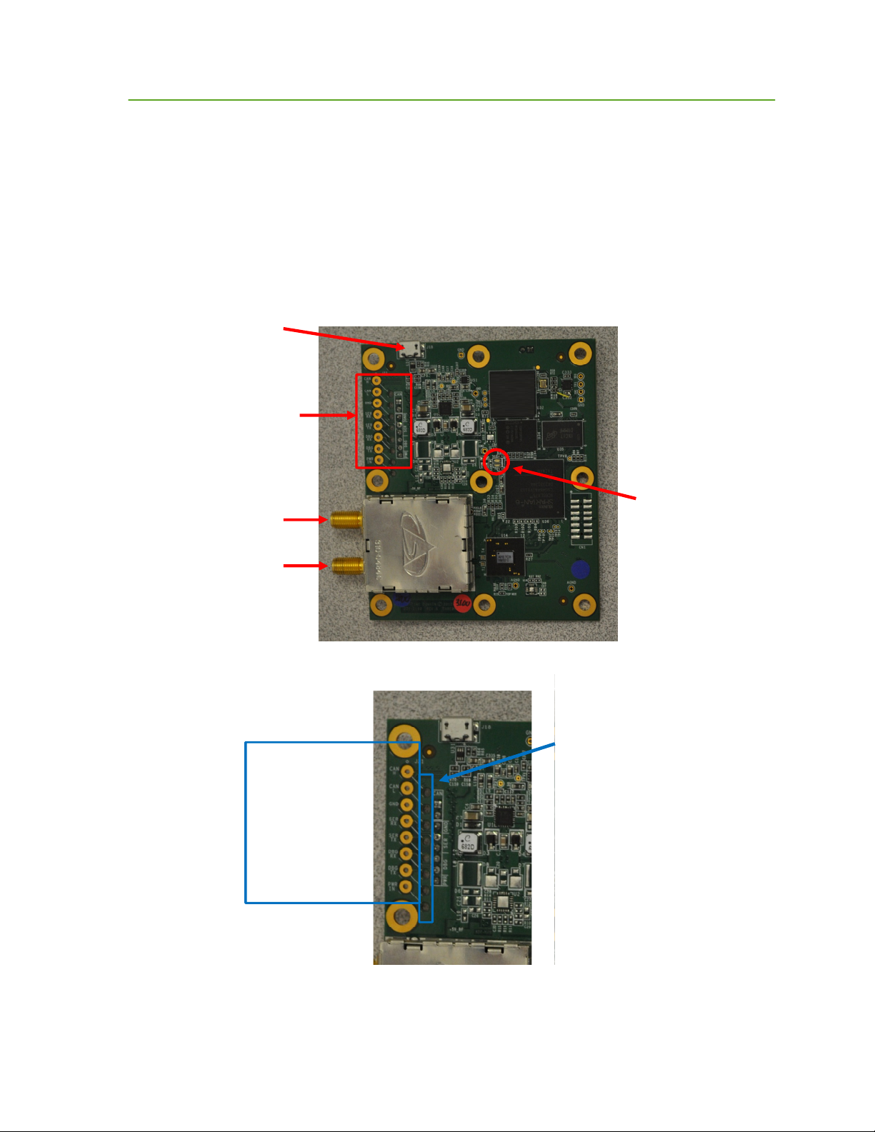
This section provides a detailed description of the various P412 interfaces. The overall board image
in Figure 5 is referenced throughout this section. The user power, serial and CAN interfaces are all
connected to the P412 via a soldered down pigtail (not provided). A set of strain relief holes is also
providing. This allows the user to lace the pigtail wires through dedicated holes before soldering to
the pad. This is detailed in Figure 6.
USB 2.0, Micro
Pigtail
Landings:
Power,
Serial,
CAN
RF B
RF A
Fig. 5: Photo of the P412 highlighting key interfaces
PIGTAIL LANDINGS:
CAN H
CAN L
GND
SER RX
SER TX
Debug RX
Debug TX
PWR IN
FPGA LEDs
STRAIN RELIEF
HOLES
Fig. 6: Pigtail mounting and strain relief holes.
Note that Debug RX and Debug TX are for manufacturing test only.
Page 10

10 P412 User’s Manual & Data Sheet
4.1 Indicator Lights
The P412 is provided with two indicator LEDs mounted adjacent to the Digital Baseband FPGA. See
Figure 5 for exact locations.
The amber LED toggles at 1Hz to indicate that the FPGA has passed Built-In Test (BIT). If the
FPGA fails BIT, then the amber LED will blink at approximately 10 Hz. The green LED is initially
off indicating that the FPGA has not been loaded. It blinks rapidly to indicate that the FPGA has
been loaded and is getting a clock. After that, a steady on or off indicates a failure.
4.2 USB, Serial and CAN Interfaces
The P412 offers three different interfaces that allow users to control the module according to their
specific application needs. The standard interfaces supported by the system are: USB 2.0 through a
Micro-B USB connector, a 3.3V TTL-level serial interface and a CAN interface. The Serial and
CAN interfaces are physically connected to the board through a user supplied pigtail. The details of
the pigtail connection are shown in Figure 6.
Note the USB connection does not provide enough power to support the RCM.
The protocol used to communicate with the P412 is fully defined in the API Specification. Connection
to the Serial and USB interfaces are described in Time Domain application note Using the P4xx USB
and Serial Interfaces.
4.3 Antenna Ports
The P412 has two antenna ports, designated Port A and Port B. The connector used on each port is a
standard polarity female SMA connector (Digi-Key part number J801-ND). The two ports enable
single and dual antenna modes of operation.
An RF transfer switch on the P412 controls how the RF electronics are connected to the SMA
connector. Normal operation is either 1) Transmit/Receive on Port A or 2) Transmit of A, Receive on
B. Use of a transfer switch allows for future operational capability.
The P412 is intended to be used with the Broadspec antenna. Using any other antenna will require
FCC recertification. However, it is possible to add passive extension cables between the antenna port
and the antenna. Be aware that using alternate UWB antennas will likely change the RF time-offlight electrical distance between the antenna port and the phase center of the antenna. Failure to
account for such changes will result in an offset or bias error in range measurements. See the RCM
API Specification for details on how the electrical distance is defined and calibrated.
Page 11
P412 User’s Manual & Data Sheet 11
5 Mechanical
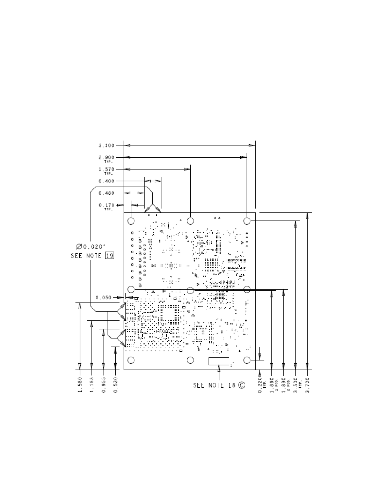
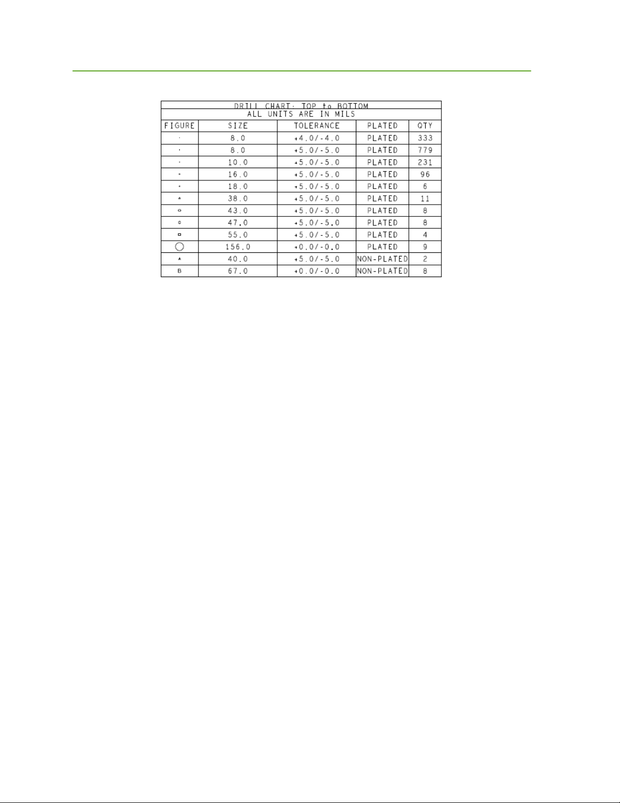
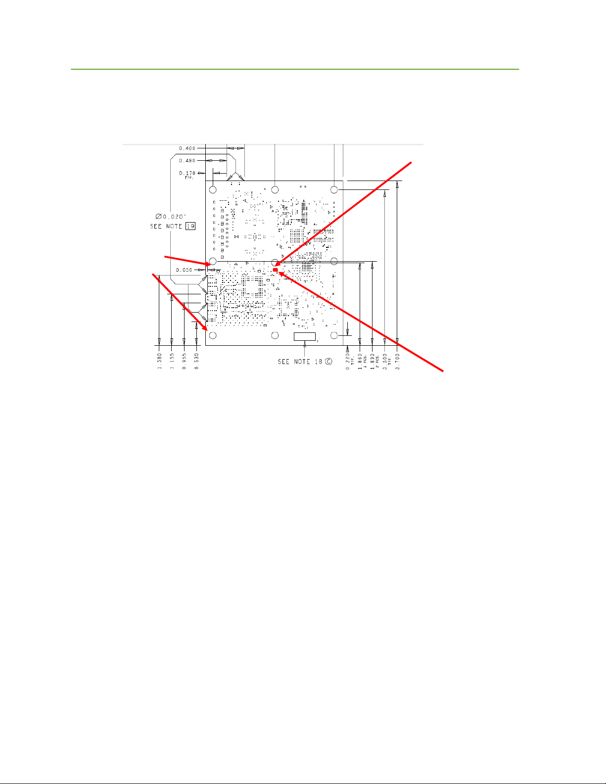
Board outlines and mounting hole locations are indicated in Figure 7 and the hole dimensions are
shown indexed in Figure 8. The nine mounting holes are sized for a #6 screw. It is anticipated that
the number of mounting holes, size of the holes and placement separations are sufficient to satisfy
most vibration requirements. All units are English/Imperial.
Fig. 7: P412 mechanical top view
Page 12
12 P412 User’s Manual & Data Sheet
Fig. 8: Hole sizes: Index table
The user must provide a sufficiently sized heat sink such that the temperatures of the board can be
kept below the maximum allowable temperature for the target deployment environment.
Most of the heat is generated by the AFE chip. There are two means by which this heat can be
extracted from the board. First, a heat sink can be placed directly in contact with the AFE. While
this will work, it should be noted that most of the heat generated by the AFE is transported to the
board through the BGA balls on the AFE. While heat can escape through the top of the chip, the
transfer characteristics of silicon are poor. Once the board begins to heat, the temperature of the RF
shield will rise. This offers the second opportunity to extract heat from the board. Because the RF
shield is tightly connected to the board ground plan, connecting the shield to the heat sink will greatly
increase the rate at which heat is transferred from the P412.
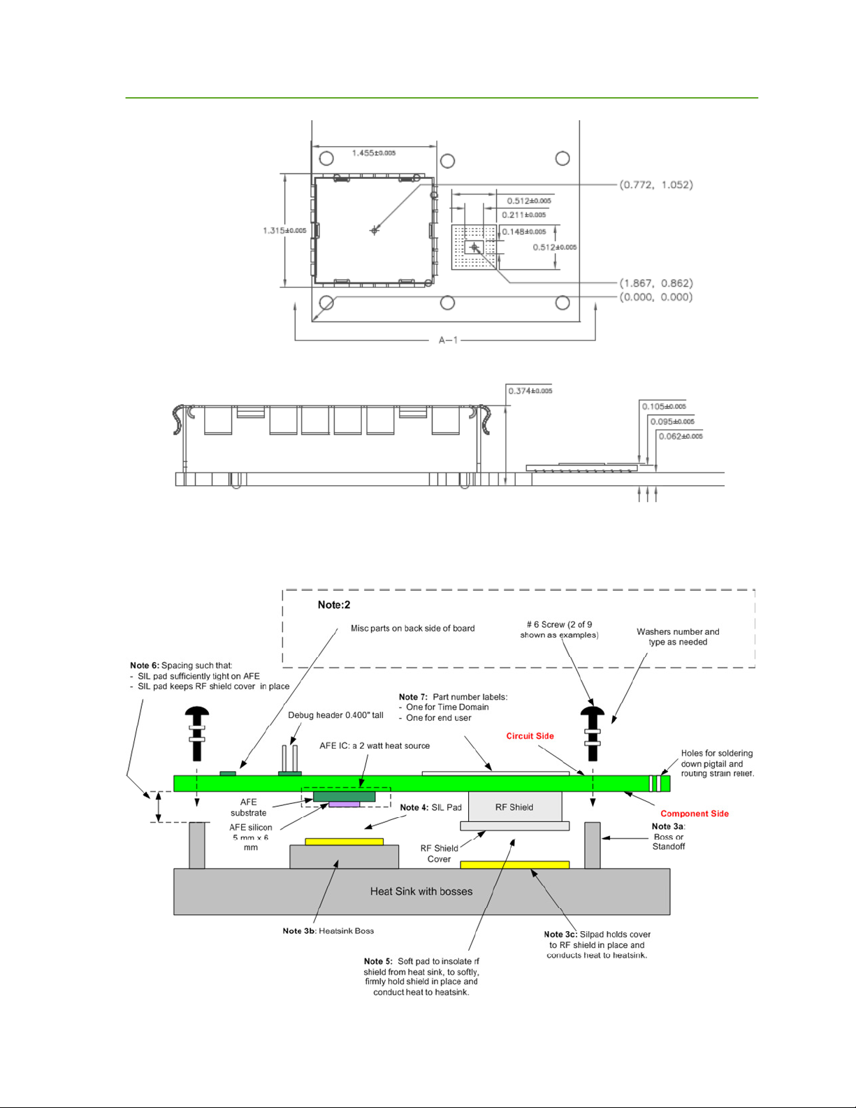
Figure 9 shows the mechanical dimensions for both the AFE and the RF Shield. Figure 10 shows a
notional heat sink strategy and calls out dimensions of relevant structures. Figure 11 shows relevant
clearances.
Page 13
P412 User’s Manual & Data Sheet 13
Fig. 9: Shield and AFE mechanical location and dimensions.
Fig. 10: Notional heat sink strategy.
Page 14
14 P412 User’s Manual & Data Sheet
Topside View
Back side clearance
between boss
landing and part is
22mil.
Backside clearance
between 262mil
Topside clearance
between boss and
shield 40mil
screw head and part
is 41mil
All other boss clearances (top and back) are at least 50mil
Fig. 11: Relevant clearances.
Part on backside
Page 15

P412 User’s Manual & Data Sheet 15
Physical Parameters
Dimensions
: 3.1”x 3.7” (7.9 x 9.4 cm)
Weight
: 58 grams
Storage
Temperature
: -
40C to 85
oC
Max
c
omponent
operating
temperatures
-
40C to 85
oC
(industrial range)
Max
allowable
board temperature:
75oC (
as reported by on bo
ard temp sensor
and using
Humidity:
Up to 95%, non
-
condensing
Input
Power
Range
: 5.75V to 30V DC
Input Power Ripple:
100 mV pk
-pk
Power
/Temp
operating a
s a Ranging
Maximum
Power Consumption:
3.8 Watts
Typical Power Consumption and
- Active (re
questing
or receiving
) 3.8
Watts
- IDLE
2.7 Watts
(Enter: 1.2ms, Exit: 1.2 ms)
- Standby_E
2.6 Watts
(Enter: 1.2 ms, Exit: 2.9 ms)
- Sta
ndby_S
2.6 Watts
(Enter: 1.3 ms, Exit: 2.9 ms)
User Interfaces/Devices
Standard PC/Laptop Interface:
USB
2.0A Client
–
Micro B connector
Serial Interface
: 3.3V TTL Serial UART 115.2kbps, 8, n, 1
CAN
Interface:
Tested up to 1 Mbps
On Board Temperature Sensor
-
40oC to 125
o
C, +/
- 2.0
o
C
RF Characteristics
Operating Band:
3.1GHz to 5.3 GHz
Center Freq:
4.3 GHz
Max
Transmit power
density
: Meets
FCC Limit
(-41.3dBm/MHz
)
Max power into base of antenna:
-13dB
m
Adjustability range:
-32
to -13dBm
Antenna Ports A&B:
Standard 50 Ohm SMA coaxial connector
Antenna Supported
Broadspec
TM
Toroidal Dipole Antenna
Antenna Control:
User cross
-
bar configured as either Tx/Rx on
p
ort A or
Noise Figure:
4.8 dB
6 Performance Specs
Table 2 summarizes the P412 specifications and key performance parameters.
P412 Specs Value
ratings:
optimum heat sink)
Radio
Transition times (power function of
communications interface):
(19 dB in 63steps)
Tx on A, receive on B. Other configurations may be
supported in the future.
Page 16

16 P412 User’s Manual & Data Sheet
Dynamic Range:
Integration: 1 (instantaneous)
30 dB
Integration: 16:1 (PII=4)
42 dB (Min Ranging Integration)
Integration: 64:1 (PII=6)
48 dB (Min Radar Integration)
Integration: 1024:1 (PII=10)
60 dB (Max Ranging Integration)
Integration: 32768:1 (PII=15)
75 dB (Max Radar Integration)
Pulse Repetition Rate
(Nominal)
10
MHz
RF Communications
Channelization:
7 user selectable pseudo
-
random pulse interval
Raw Data (Symbol) rates:
See Table 3:
Max Range (
max
FCC Part 1
5
See Table 3:
Comms type:
Packet transmission
Max user bytes/packet:
1024
Pulse integration rates (PII):
4 (16:1), 5
(32:1), 6 (64:1), 7 (128:1) 8 (256:1),
Ranging
Performance
Ranging techniques:
Pulsed Two
-
Way Time
-of-
Flight (TW
-
TOF),
Two
-
Way Time
-of-
Flight
Line of Sight Range Performance
See Note 1
Precision (Standard Deviation)
2.3 cm
Accuracy (Bias error):
2.1 cm
Range Update Rate
See Table 3
Non-Line of Sight Performance
See Note 2
Coarse Range Estimation (LOS only
) See Note 3
Range update rate
See Table 3
channels. Others available for special applications.
transmit power, standard
Broadspec Antennas, free
space, thermally noise limited
environment, clear line of
sight)
9 (512:1), 10(1024:1)
Coarse Range Estimation (CRE)
Table 1: P412 performance characteristics
Note 1: Precision and Accuracy in LOS conditions. The Line of Sight (LOS) Precision and
Accuracy specification is based on a measurement campaign that included 20,000 range
measurements taken in an open field, over an operating range that varied from 2 ft. to 300 ft., for PIIs
4 through 8 inclusive, at minimum and maximum transmit gain, when the received signal was linear
and also when it was in compression. The quoted values are the results of the composite of all of the
measurements. This includes combinations of settings that may not be reasonable (e.g., operation at
minimum range and maximum transmit power). It is believed to be a conservative estimate of the
system’s ranging Precision and Accuracy. When averaging many range measurements, users have
reported precisions on the order of a few millimeters.
Note 2: Precision and Accuracy in NLOS conditions. Time Domain does not have a specification
for accuracy in Non-Line of Sight (NLOS) environments. This is because of the wide variety of
conditions that can be encountered. For example, if one is measuring range inside a building that is
Page 17

P412 User’s Manual & Data Sheet 17
4 35 632k
6.5 ms, 15
4 Hz
5 60 316k
8.5 ms, 118 Hz
6 88 158k
12.5 ms, 80 Hz
7 125 79k 20 ms, 50 Hz
8 177 39.5k
36 ms, 28 Hz
9 250 19.7k
67 ms, 15 Hz
10 354 9.86k
132 ms, 8 Hz
constructed of wood frame and drywall (aka sheetrock or gypsum board), then one will experience a
level of performance that is less than but close to LOS conditions. This is because wood and drywall
do not significantly attenuate or disperse RF signals at the P412’s operating frequency. At the
opposite end of the propagation spectrum would be operation inside a metal ship. Because metal
blocks radio frequencies, the operating range would be limited to the size of the room. Operation in
NLOS must be determined empirically. Having said that, we routinely measure range from one side
of our office space to the other (a distance of 30 meters through an environment that is not only
NLOS but is also occluded by large amounts of metal) with an accuracy of better than +/- 1 meter.
PII Max Range
(meters)
Table 2: Data and ranging performance characteristics
Data rate:
(bps)
Precision Range Measurement
(time, rate)
Note that these are conservative estimates of range performance and have a healthy safety margin
allowing robust performance. For example, with PII set to 9, Time Domain has routinely achieved
650 meters in clear line of sight conditions over open ground.
Note 3: Precision and Accuracy of CRE: There are three main factors that affect the Precision and
Accuracy of a CRE measurement: stability of the RF channel, signal strength, and changes in antenna
pattern. If RF channel characteristics are stable, then the accuracy of the CRE measurement should
be close to that of the reference PRM range measurement. However, if the RCM is physically
moving, with associated antenna pattern changes, then the RF channel will change with time.
Therefore, the recalibrating PRM measurements should be taken frequently enough such that the rate
of change (“drift”) of the RF channel will be small. This rate of change will vary with node speed
and change in orientation and must be determined empirically. Random effects, along with sampling
variability, can cause a static node’s signal strength measurement to vary as much as 10%. The CRE
error is also a function of distance/SNR as a smaller/farther signal contains a higher proportion of
noise elements. This translates into a CRE standard deviation error of approximately 10% at short
distances growing up to 30% at very long distances.
Note 4: Setting the transmit power level: The maximum transmit power provided by the P412 will
be at the limit allowed by the FCC. The user has the option to reduce the transmit power from this
maximum and operate at levels as much as 19dB below the limit. This adjustment is made through
the API “Set Configuration” command. Alternatively, this adjustment can be made through the
Graphic User Interface (GUI) RCM RET by modifying the “Transmit Gain” setting on the Config
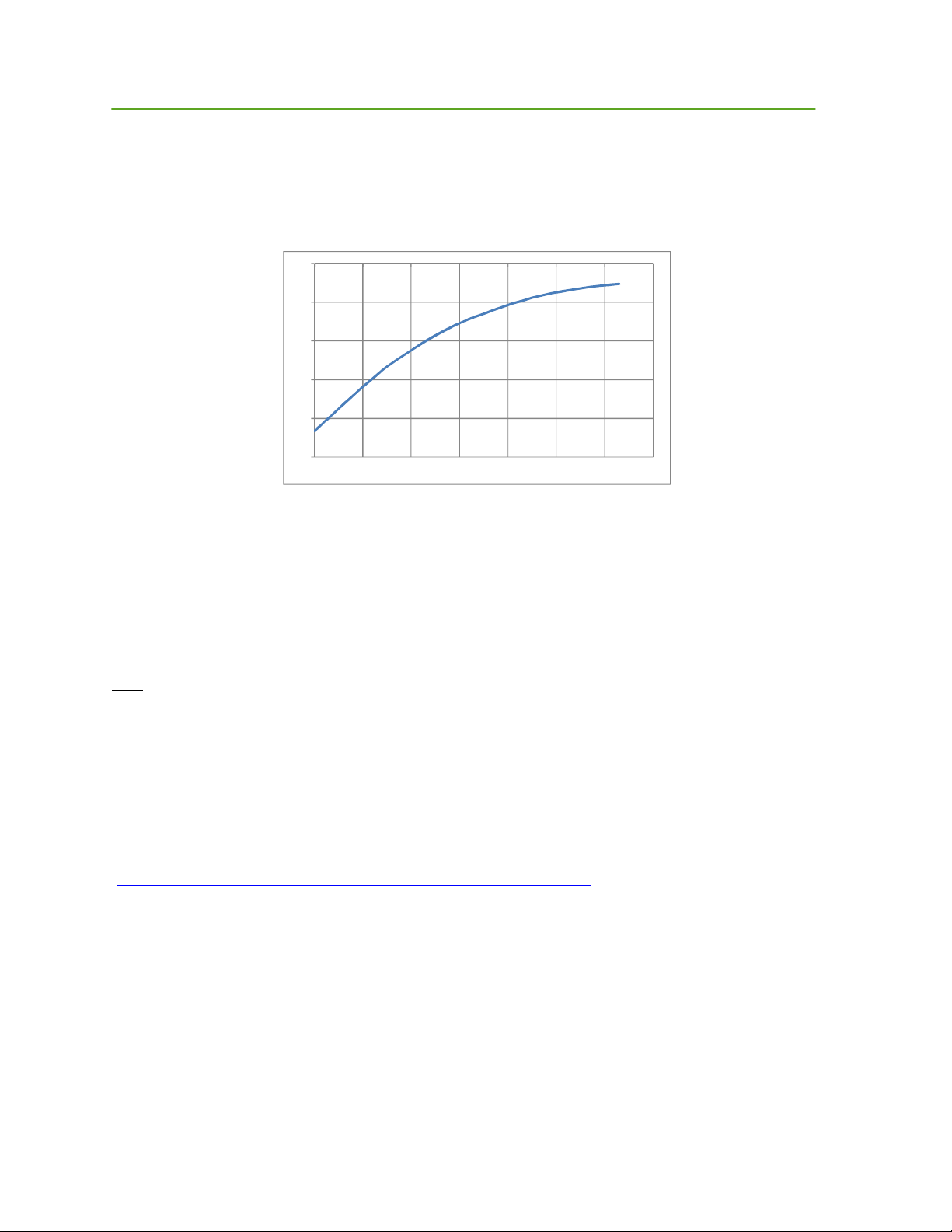
Tab. Figure 12 shows the relationship between the value selected for Transmit Gain and the radiated
power when using a standard P412. This measurement was taken by directly connecting the output of
Page 18
18 P412 User’s Manual & Data Sheet
the P412 to a power meter. The maximum level shown in Figure 12 (-13 dBm at a gain setting of
63) corresponds to the maximum level permitted by FCC when used with the Broadspec antenna. It
is not possible for the user to enter a value greater than 63. Using any antenna other than the
Broadspec invalidates the certification.
-10
-15
-20
-25
-30
-35
P400 Transmit Power (EIRP dBm)
0 10 20 30 40 50 60 70
MRM/RET Transmit Gain Setting
Figure 12: Transmit power as a function of Transmit Gain setting. (Setting 63 = FCC limit)
7 Broadspec Antenna
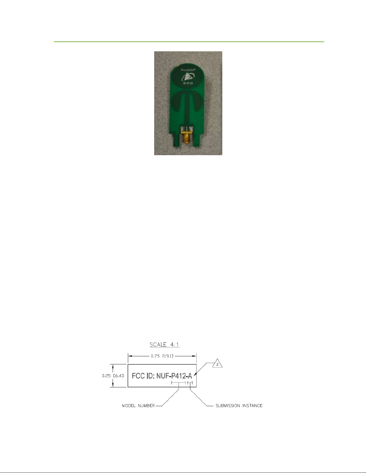
The P412 is designed to operate with the Broadspec P200 antennas shown in Figure 13. Use with
ANY other antenna invalidates the FCC certification. Per FCC 15.203, the Broadspec antenna must be
professionally installed and the installer has the responsibility to insure that the Broadspec antenna is
used.
The P412 can be operated with a single antenna (used for transmit and receive) or with two antennas
(where one is dedicated for transmit and the second for receive).
The Broadspec Ultra Wideband Antenna (~3dBi) provides an omni-directional transmit/receive
pattern supporting a frequency range of 3.1-5.3 GHz. It has a standard SMA female connector and
measures 1”x 2.5” x 0.125”. Specifications available on the web at:
http://www.timedomain.com/datasheets/TD_Broadspec_Antenna.pdf
Page 19
P412 User’s Manual & Data Sheet 19
Figure 13: Broadspec Antenna with right angle connector
8 FCC Compliance
The P412 and associated Broadspec antenna have been designed to be in compliance with the Federal
Communications Commission (FCC) regulations governing both UWB hand-held systems (Part
15.519) also known as “battery powered devices” and UWB Surveillance Systems (Part 15.511).
This means that the device can be incorporated in a wide variety of products including mobile
tracking systems, mobile locators, radar-based locators, guidance and position systems, radar fences
and communication devices.
More specifically,
This device complies with part 15 of the FCC Rules. Operation is subject to the following
two conditions: (1) This device may not cause harmful interference, and (2) this device must
accept any interference received, including interference that may cause undesired operation.
The label which provides the certification number is shown below in Figure 14.
Figure 14: FCC ID number
Page 20
20 P412 User’s Manual & Data Sheet
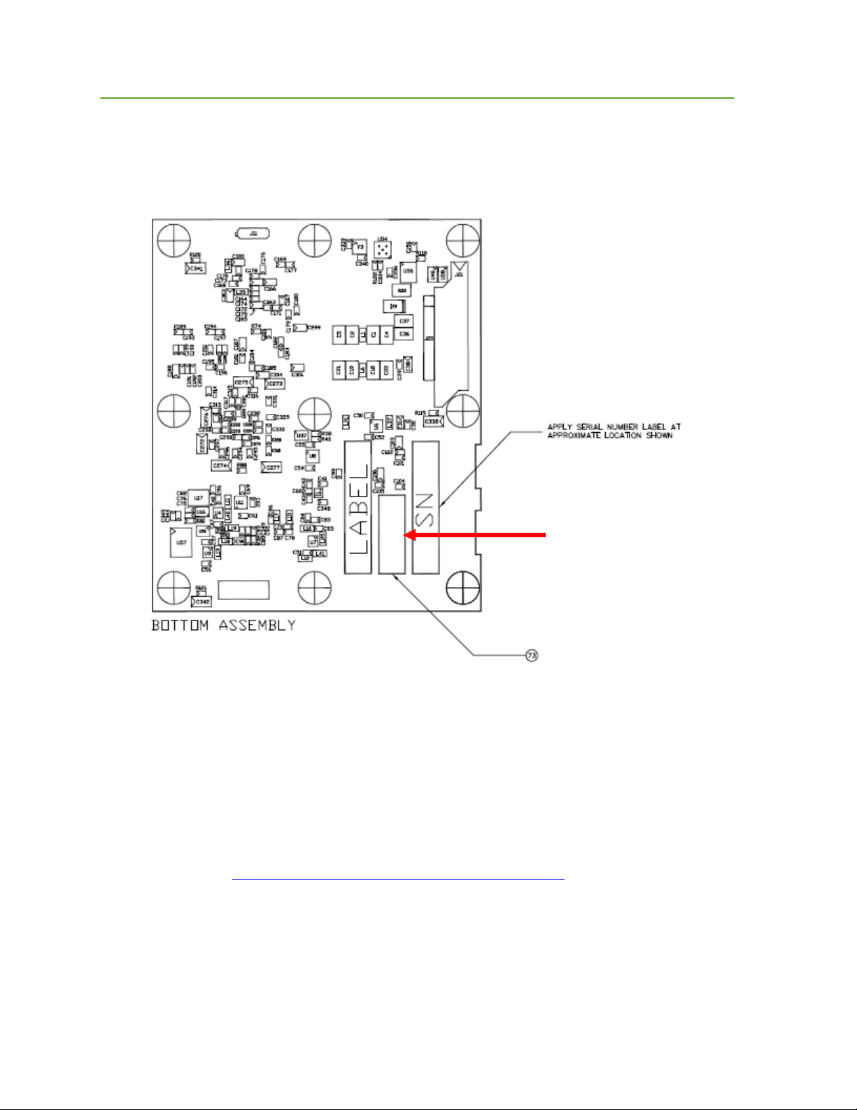
This label is located on the back or bottom side of the P412. See Figure 15.
FCC ID Label
Figure 15: Location of certification number
9 Export Restrictions
Relating to export, the Department of Commerce’s Bureau of Industry and Security has assigned the
Export Commodity Control Number (ECCN) of 5A001b.4 to the P412. Products falling under
ECCN 5A001b.4 are controlled for export purposes pursuant to the Commerce Control List for
National Security and Antiterrorism. For the latest information from the Commerce Department on
Export, please go to: http://www.bis.doc.gov/licensing/exportingbasics.htm.
 Loading...