

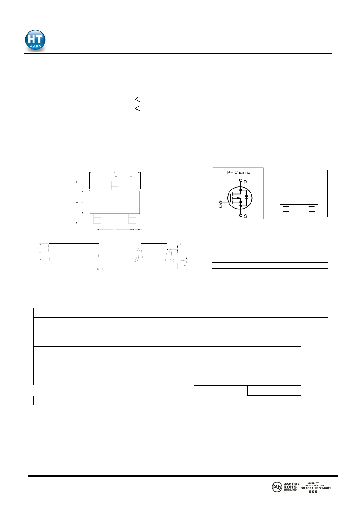
20V P-Channel Enhancement Mode MOSFET
XP152A12COMR
VDS= -20V
RDS(ON), Vgs@-4.5V, Ids@-2.8A
RDS(ON), Vgs@-2.5V, Ids@-2.0A
130m
190m
Ω
Ω
Features
Advanced trench process technology
High Density Cell Design For Ultra Low On-Resistance
Package Dimensions
SOT-23(PACKAGE)
REF.
A 2.70 3.10 G 1.90 REF.
B 2.40 2.80 H 1.00 1.30
C 1.40 1.60 K 0.10 0.20
D 0.35 0.50 J 0.40 E 0 0.10 L 0.85 1.15
F 0.45 0.55 M
Millimeter
Min.
Max.
Maximum Ratings and Thermal Characteristics (TA = 25oC unless otherwise noted)
G
REF.
D
S
Millimeter
Min. Max.
0° 10°
Parameter Symbol Limit
Drain-Source Voltage
Gate-Source Voltage
Continuous Drain Current
Pulsed Drain Current
Maximum Power Dissipation
Operating Junction and Storage Temperature Range
Junction-to-Ambient Thermal Resistance (PCB mounted)
Junction-to-Ambient Thermal Resistance (PCB mounted)
Notes
1)
Pulse width limited by maximum junction temperature.
2)
Surface Mounted on FR4 Board, t v 5 sec.
3)
Surface Mounted on FR4 Board.
1)
2)
TA = 25
TA = 75oC
2)
3)
o
VDS -20
VGS ±8
I
D
-2.2
I
-8
DM
P
D
TJ, T
-55 to 150
stg
R
thJA
1
JinYu
semiconductor
www.htsemi.com
1.25
0.8
100
166
Unit
V
A
W
o
C
o
C/W
Date:2011/05
20V P-Channel Enhancement Mode MOSFET
XP152A12COMR
ELECTRICAL CHARACTERISTICS
Parameter Test Condition
Static
Drain-Source Breakdown Voltage BV
Drain-Source On-State Resistance
Gate Threshold V olt a ge V
Zero Gate Voltage Drain Current 0
Gate Body Leakage I
Forward Transcon duc t ance g
Dynamic
Total Gate Charge Q
Gate-Source Charge Q
Gate-Drain Charge Q
Turn-On Delay Time t
Turn-On Rise Time t
Turn-Off Delay Time t
Turn-Off Fall Time t
Input Capacitance C
Output Capacitance C
Reverse Transfer Cap ac it a nce C
Source-Drain Diode
Max. Diode Forward Current I
Diode Forward Voltage V
1)
Pulse test: pulse width <= 300us, duty cycle<= 2%
1)
I
1)
Symbol Min.
DSS
R
DS(on)
GS(th)
DSS
GSS
fs
g
gs
gd
d(on)
r
d(off)
f
iss
oss
rss
S
SD
Typ.
VGS = 0V, ID = -250uA -20 V
VGS = -4.5V, ID = -2.8A 105 130
VGS = -2.5V, ID = -2.0A 145 190
VDS =VGS, ID = -250uA -0.45 V
V
= -20V, VGS = 0V -1
DS
= -20V, VGS = 0V TJ=55
V
DS
VGS = ± 8V, VDS = 0V ±100 nA
VDS = -5V, ID = -2.8A 6.5 S
= -6V, ID -2.8A
V
DS
= -4.5V
V
GS
= -6V, RL=6Ω
V
DD
ID -1.A, V
^
R
G
V
DS
f = 1.0 MHz
IS = -1.6A, VGS = 0V -1.2 V
^
= -4.5V
GEN
= 6
Ω
= -6V, VGS = 0V
o
C
5.8 10
0.85
1.7
13 25
36 60
42 70
34 60
415
223
87
-0.8
Max.
-10
-1.6 A
2
JinYu
semiconductor
www.htsemi.com
Date:2011/05
Unit
mΩ
uA
nC
ns
pF

20V P-Channel Enhancement Mode MOSFET
XP152A12COMR
10
8
6
4
- Drain Current (A)I
D
2
0
012345
0.6
0.5
W )
0.4
0.3
- On-Resistance (r
0.2
DS(on)
0.1
Output Characteristics Transfer Characteristics
VGS = 5, 4.5, 4, 3.5, 3 V
0, 0.5, 1 V
VDS - Drain-to-Source Voltage (V)
On-Resistance vs. Drain Current
VGS = 2.5 V
_
2.5 V
VGS = 4.5 V
1.5 V
2 V
10
8
6
4
- Drain Current (A)I
D
2
0
0.0 0.5 1.0 1.5 2.0 2.5 3.0
VGS - Gate-to-Source Voltage (V)
1000
800
600
400
C - Capacitance (pF)
200
C
oss
C
rss
TC = -55_C
Capacitance
C
iss
25_C
125_C
1.8
1.6
W )
1.4
1.2
(Normalized)
- On-Resistance (r
1.0
DS(on)
0.8
0.6
0
036912
VDS - Drain-to-Source Voltage (V)
On-Resistance vs. Junction Temperature
VGS = 4.5 V
= 2.8 A
I
D
-50 0 50 100 150
T
- Junction Temperature (_C)
J
0.0
0246810
ID - Drain Current (A)
5
VDS = 6 V
= 2.8 A
I
D
4
3
2
- Gate-to-Source Voltage (V)
1
GS
V
0
02468
Gate Charge
Qg - Total Gate Charge (nC)
3
JinYu
semiconductor
www.htsemi.com
Date:2011/05

20V P-Channel Enhancement Mode MOSFET
XP152A12COMR
10
- Source Current (A)I
S
Variance (V)V
GS(th)
Source-Drain Diode Forward Voltage On-Resistance vs. Gate-to-Source Voltage
TJ = 150_C
TJ = 25_C
1
0.2 0.4 0.6 0.8 1.0 1.2 1.4 1.6
VSD - Source-to-Drain Voltage (V) VGS - Gate-to-Source Voltage (V)
0.4
0.3
0.2
0.1
0.0
Threshold Voltage Single Pulse Power
ID = 250 mA
0.6
0.5
W )
0.4
0.3
- On-Resistance (r
0.2
DS(on)
0.1
0.0
02468
14
12
10
8
6
Power (W)
4
Single Pulse
ID = 2.8 A
TC = 25_C
-0.1
-0.2
-50 0 50 100 150
0.1
Thermal Impedance
Normalized Effective Transient
0.01
2
1
Duty Cycle = 0.5
0.2
0.1
0.05
0.02
-4
10
TJ - Temperature (_C) Time (sec)
Normalized Thermal Transient Impedance, Junction-to-Ambient
Single Pulse
-3
10
-2
10
Square Wave Pulse Duration (sec)
10
2
0
0.01 0.10 1.00 10.00
-1
1
4
JinYu
semiconductor
www.htsemi.com
10
Date:2011/05
30

 Loading...