

HSMC H3842P, HSMC3842 Datasheet
HI-SINCERITY
MICROELECTRONICS CORP.
Spec. No. : HP200202
Issued Date : 1998.08.01
Revised Date : 2002.12.03
Page No. : 1/10
H3842P / HSMC3842
HIGH PERFORMANCE CURRENT MODE CONTROLERS
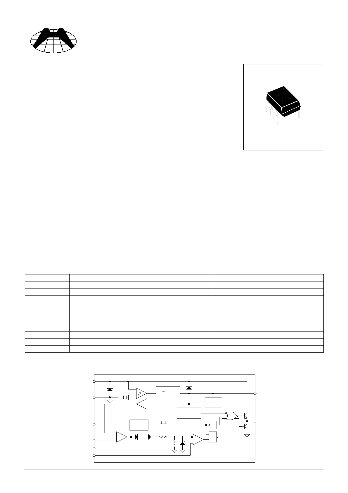
Description
The H3842P/HSMC3842 are high performance fixed frequency current mode
controllers. They are specifically designed for Off-Line and DC To DC converter
applications offering the designer a cost-effective solution with minimal external
components. These integrated circuits feature a trimmed oscillator for precise duty
cycle control. A temperature compensa-ted reference, high gain error amplifier,
current sensing comparator, and a high current totem pole output ideally suited for
driving a power MOSFET. Also included are protective features consisting of input and reference undervoltage
lockouts each with hysteresis, cycle-by-cycle current limiting, programmable output deadtime, and a latch for single
pulse metering.
Features
• Trimmed Oscillator for Precise Frequency Control
• Oscillator Frequency Guaranteed at 250 kHz
• Current Mode Operation to 500 kHz
• Automatic Feed Forward Compensation
• Latching PWM for Cycle-By-Cycle Current Limiting
• Internally Trimmed Reference with Undervoltage Lockout
• High Current Totem Pole Output
• Undervoltage Lockout with Hysteresis
• Low Startup and Operating Current
DIP-8Pin
Absolute Maximum Ratings
Symbol Parameter Value Unit
Vi Supply Voltage (low impedance source) 30 V
Vi Supply Voltage (Ii<30mA) Self Limiting
Io Output Current
±1
Eo Output Energy (capacitive load) 5 uJ
Analog Inputs (pin 2, 3) -0.3 to 5.5 V
Error Amplifier Output Sink Current 10 mA
Ptot
Power Dissipation at Tamb≤25
o
C
1.25 W
Tstg Storage Temperature Range -65 to 150
TJ Junction Operating Temperature -40 to 150
TL Lead Temperature (soldering 10s) 300
Block Diagram
Vcc
Ground
RT/CT
VFB
COMP
Current
Sense
7
5
4
2
1
3
34V
Error AMP.
+
-
2.50V
UVLO
OSC
S/R
2R
5V
REF
R
VREF Good
Logic
1V
Comparator
Current
Sense
Internal
Bias
T
S
R
PWM Latch
8
6
VREF
5V 50mA
Output
A
o
C
o
C
o
C
H3842P HSMC Product Specification
HI-SINCERITY
MICROELECTRONICS CORP.
Pin Connection (Top View)
DIP-8P Function Description
This pin is the Error Amplifier output and is made available for
loop compensation.
This is the inverting input of the Error Amplifier. It’s normally
connected to the switching power supply output through a
resistor divider.
A voltage proportional to inductor current is connected to this
input. The PWM uses this information to terminate the output
switch conduction.
The oscillator frequency and maximum output duty cycle are
programmed by connecting resistor RT to Vref and cpacitor CT
to ground. Operation to 500kHz is possible.
This output directly drives the gate of a power MOSFET. Peak
currents up to 1A are sourced and sunk by this pin.
This is the reference output. It provides charging current for
capacitor CT through resistor RT.
5678
1234
Pin1: Compensation
Pin2: Voltage Feedback
Pin3: Current Sense
Pin4: RT/CT
Pin5: Ground This pin is the combined control circuitry and power ground.
Pin6: Output
Pin7: Vcc This pin is the positive supply of the control IC.
Pin8: Vref
Spec. No. : HP200202
Issued Date : 1998.08.01
Revised Date : 2002.12.03
Page No. : 2/10
Thermal Data
Symbol Description Max. Units
Rth j-amb Thermal Resistance Junction-ambient 100
Electrical Specifications
Parameter Test Conditions Min. Typ. Max. Units
Under-Voltage Lockout Sect ion
Start Threshold 14.5 16 17.5 V
Min. Operating Voltage After Turn On 8.5 10 11.5 V
Electrical Characteristics
Unless otherwise stated, specifications apply for 0≤Ta≤70°C Vcc =15V (Note 1); RT=680Ω, CT=0.022uF for
triangular mode, RT=10k, CT=3.3nf for sawtooth mode
Parameter Test Conditions Min. Typ. Max. Units
Reference Section
Reference Output Voltage
Line Regulation
Load Regulation
Temperature. Stability
Total Output Variation Line , Load , Temp (Note 2) 4.82 - 5.18 V
Output Noise Voltage
Long Term Stability
Output Short current
Oscillator Section
Frequency
Frequency Chnge with Temperature
Frequency Change with Temperature
Oscillator Voltage Swing Peak to Peak - 1.7 - V
Discharge Current
Tj=25°C,Io=1mA
12V≤Vin≤25V
1mA≤Io≤20mA
(Note 2)
10Hz≤f≤10kHz,Tj=25°C
Ta=125°C,1000Hrs
Ta=25°C
Tj=25°C
Tlow≤Ta≤Thigh
12V≤Vcc≤25V
Tlow≤Ta≤Thigh (Note 2)
Tj=25°C
Tj=25°C
Tlow≤Ta≤Thigh
(Note 2)
(Note 2)
4.90 5 5.1 V
-2.020mV
-3.025mV
-0.2-
-50- uV
-5-mV
-30 -100 -180 mA
47 52 57 KHz
46 52 60 KHz
-0.21 %
-5-%
-0.5- %
7.8 8.3 9.3 mA
7.2 - 9.5 mA
mV/°C
o
C/W
H3842P HSMC Product Specification
HI-SINCERITY
MICROELECTRONICS CORP.
Spec. No. : HP200202
Issued Date : 1998.08.01
Revised Date : 2002.12.03
Page No. : 3/10
Parameter Test Conditions Min. Typ. Max. Units
Error Amplifier Section
Voltage Feedback Input Vo=2.5V 2.42 2.50 2.58 V
Input Bias Current VFB=5.0V - -0.1 -2.0 uA
Open Loop Voltage Gain
Unity Gain Bandwidth
Power Supply Rejection Ratio
Output Current
Output Voltage Swing
High State
2≤Vo≤4 V
Tj=25°C
(Note 2)
12V≤Vcc≤25V
Sink (Vo=1.1V, VFB=2.7V) 2.0 12 - mA
Source (Vo=5.0V, VFB=2.3V) -0.5 -1.0 - mA
VFB=2.3V, RL=15K to ground 5 6 - V
65 90 - dB
0.7 1.0 - MHz
60 70 - dB
Low State VFB=2.7V, RL=15K to Vref - 0.7 1.1 V
Current Sense Section
Current Sense Input Voltage Gain
Maximum Current Sense Input
Thresold
Ppwer Supply Rejection Ratio
(Notes 3 & 4)
(Note 3)
12V≤Vcc≤25V
(Note 3)
2.85 3.0 3.15 V/V
0.9 1.0 1.1 V
-70- dB
Input Bias Current - -2.0 -10 uA
Propagation Delay
Tj=25°C
(Note 2)
- 150 300 nS
Output Section
Low State (Isink=20mA) - 0.1 0.4 V
Output Voltage
Low State (Isink=200mA) - 1.5 2.2 V
High State (Isource=20mA) 13 13.5 - V
High State (Isource=200mA) 12 13.4 - V
Output Voltage Rise Time
Output Voltage Fall Time
Tj=25°C, CL=1.0nF
Tj=25°C, CL=1.0nF
(Note 2)
(Note 2)
- 50 150 nS
- 50 150 nS
Output Voltage with UVLO Activated Vcc=6V , Isink=1.0mA - -0.1 -1.1 V
Total Device
Start-Up Current - 0.1 0.5 mA
Operating Supply Current Vpin2=Vpin3=0, RT=10K, CT=3.3nF - 11 17 mA
Vcc Zener Voltage Icc=25 mA - 34 - V
Note 1: Adjust Vcc above the start threshold before setting at 15V.
Note 2: These parameters, although guaranteed are not 100% tested in production.
Note 3: Parameter measured at trip point of latch with Vpin2=0.
Note 4: Gain defined as: A=Vpin1/Vpin3, 0≤Vpin3≤0.8V
H3842P HSMC Product Specification
 Loading...