

HSMC HM772A Datasheet
HI-SINCERITY
MICROELECTRONICS CORP.
Spec. No. : Preliminary Data
Issued Date : 2000.12.01
Revised Date : 2001.01.01
Page No. : 1/3
HM772A
PNP EPITAXIAL PLANAR TRANSIST OR
Description
The HM772A is designed for use in output stage of amplifier, voltage
regulator, DC-DC converter and driver.
Absolute Maximum Ratings
Maximum Temperatures
•
Storage Temperature....................................................................................................... -55 ~ +150 °C
Junction Temperature ............................................................................................... +150 °C Maximum
Maximum Power Dissipation
•
Total Power Dissipation (Ta=25°C) ........................................................................................1 W
Total Power Dissipation (Ta=25°C)........................................................................................ 2 W
Total Power Dissipation (Ta=25°C)..................................................................................... 1.5 W
Maximum Voltages and Currents (Ta=25°C)
•
VCBO Collector to Base Voltage.................................................................................................... -60 V
VCEO Collector to Emitter Voltage ................................................................................................. -50 V
VEBO Emitter to Base Voltage......................................................................................................... -5 V
IC Collector Current (continuous)..................................................................................................... -3 A
IC Collector Current (pulse)................................................................................................. -7 A
Note1: When tested in free air condition, without heat sinking.
Note2: When mounted on a 40X40X1mm ceramic board.
Note3: Printed circuit board 2mm thick, collector plating 1cm square or larger.
Note4: Single pulse PW=1ms
(Note1)
(Note2)
(Note3)
(Note4)
Characteristics
Symbol Min. Typ. Max. Unit Test Conditions
BVCBO -60 - - V IC=-100uA
BVCEO -50 - - V IC=-1mA
BVEBO -5 - - V IE=-10uA
ICBO - - -1 uA VCB=-30V
IEBO - - -1 uA VEB=-3V
*VCE(sat) - -0.3 -0.5 V IC=-2A, IB =-0.2A
*VBE(sat) - -1 -2 V IC=-2A, IB=-0.2A
*hFE1 30 - - VCE=-2V, IC=-20mA
*hFE2 100 160 500 VCE=-2V, IC=-1A
fT - 80 - MHz VCE=-5V, IC=-100mA, f=100MHz
Cob - 55 - pF VCB=-10V, f=1MHz
(Ta=25°C)
*Pulse Test : Pulse Width ≤380us, Duty Cycle≤2%
Classification Of hFE2
Rank Q P E
Range 100-200 160-320 250-500
HSMC Product Specification
HI-SINCERITY
MICROELECTRONICS CORP.
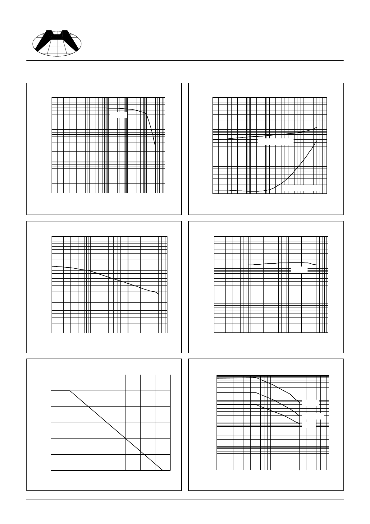
Characteristics Curve
Spec. No. : Preliminary Data
Issued Date : 2000.12.01
Revised Date : 2001.01.01
Page No. : 2/3
1000
Current Gai n & Collector Current
VCE=2V
100
hFE
10
1
0.01 0.1 1 10 100 1000 10000
1000
100
Capacitance & Reverse-Biased Volt age
Collector Curren t (m A )
10
Saturation Volt age & Coll ector Current
1
BE(sat)
V
0.1
Saturation Voltage (V)
0.01
0.01 0.1 1 10 100 1000 10000
1000
100
Cut off Fr equency & Collector Cu rrent
Collector Current (mA)
@ IC=10I
V
B
CE(sat)
VCE=5V
@ IC=10I
B
Capac itanc e (pF)
10
1
0.1 1 10 100
Reverse-Biased Vol t ag e ( V)
Cob
Power Derating
1200
1000
800
600
400
Power Dissipation-PD(mW)
200
0
0 20 40 60 80 100 120 140 160
Ambient Temperature-Ta(oC)
10
Cutoff Frequency (MHz)
1
1 10 100 1000
Collector Current (mA)
Sa fe Operating Area
10000
1000
(mA)
C
100
Collector Current-I
10
1
1 10 100
Forwar d Biased Vol tage-VCE (V)
PT=1ms
PT=100ms
PT=1s
HSMC Product Specification
 Loading...