

HSMC H7808BM, H7808AM Datasheet
HI-SINCERITY
MICROELECTRONICS CORP.
Spec. No. : Preliminary Data
Issued Date : 1998.08.01
Revised Date : 2001.01.30
Page No. : 1/3
H7808AM
H7808BM
Low Current Positive Voltage Regulator Of Surface Mount Device
Description
The H7808_M series of surface mount device regulators are easyto-use devices suitable for multitude of applications that require a
regulated supply of up to 100mA. These regulators feature internal current limiting and thermal
shutdown making them remarkably rugged. No external components are required with the 7808_M devices in many applications.
These devices offer a substantial performance advantage over the traditional zener diode
resistor combination, as output impedance and quiescent current are substantially reduced.
Wide Range Of Available, Fixed Output Voltages
•
Internal Short-Circuit Current Limiting
•
Internal Thermal Overload Prot ecti on
•
No External Components Required
•
Absolute Maximum Ratings
Input Voltage................................................... 30 V (5V Through 9V), 35 V (12V Through 18V)
•
Total Power Dissipation ........................................................................................... Internal limit
•
Operating Temperature Range............................................................................ 0 °C to +70 °C
•
Maximum Junction Temperature...................................................................................... 125 °C
•
Storage Temperature Range .......................................................................... -55 °C to +150 °C
•
Lead Temperature (Soldering 10S).................................................................................. 260 °C
•
(Ta=25°C)
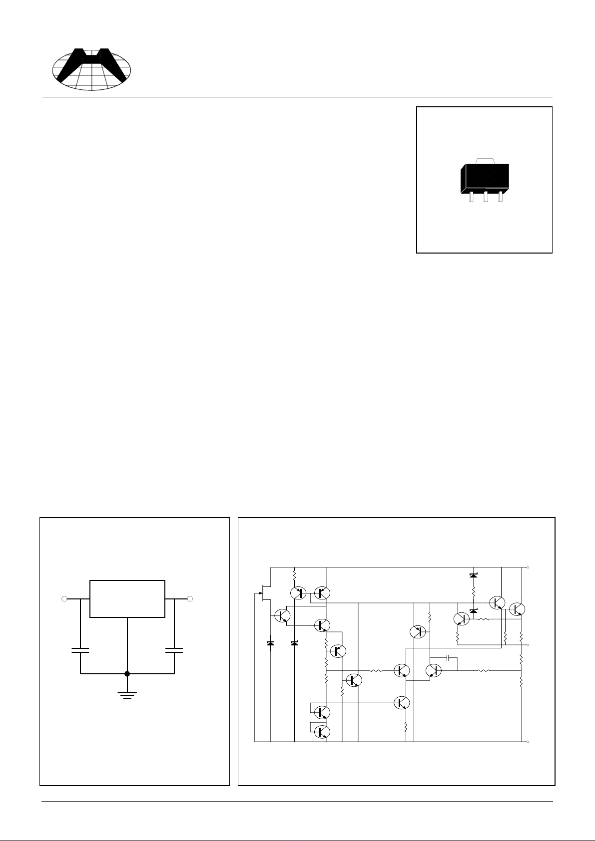
Typical Application Schematic Diagram
Vin
VoutVin
H7808_M
C1 C2
3.41K
3.89K
5.7K
576
13K
7.8K
5K
100
100
5pF
1.5K 1.9K
2.23K
Vout
A common ground is required between the input
and the output voltages. The input voltage must
remain typically 2.0V above the output voltage
even during the low point on the input ripple
voltage.
Note : C1 and C2 are required if regulator is
located far from power supply filter and load, or
H7808AM, H7808BM HSMC Product Specification
2.84K
GND
HI-SINCERITY
MICROELECTRONICS CORP.
Electrical Characteristics
Vin=14V, Io=40mA, Tj=25°C Cin=0.33uF, Cout=0.1uF (unless otherwise noted)
Spec. No. : Preliminary Data
Issued Date : 1998.08.01
Revised Date : 2001.01.30
Page No. : 2/3
Symbol Parameter Conditions
Tj=25°C
Vo Output Voltage
10.5V≤Vin≤23V
1mA≤Io≤40mA
1mA≤Io≤70mA
Vo
∆
Vo
∆
Line Regulation
Load Regulation
IQ Quiescent Current
IQ
∆
Quiescent Current
Change
Vn Output Noise Voltage
Vin / ∆Vout
∆
Isc
Ripple Rejection
Peak Output / Short -
Circuit Current
VD Dropout Voltage
Tj=25°C, 10.5V≤Vin≤23V
Tj=25°C, 11V≤Vin≤23V
Tj=25°C, 1mA≤Io≤40mA
Tj=25°C, 1mA≤Io≤100mA
Tj=25°C
1mA≤Io≤40mA
11V≤Vin≤23V
Ta=25°C, 10Hz≤f≤10KHz
11V≤Vin≤21V, f=120Hz
Tj=25°C
Tj=25°C
H7808AM
Min Typ Max
Units
7.76 8 8.24
7.76 8 8.24
V
7.76 8 8.24
-80175
-70125
-840
-1580
mV
mV
-25.5mA
--0.1
-1.5
mA
-60-uV
39 45 - dB
- 140 - mA
-1.7- V
H7808BM
Min Typ Max
Units
7.7 8 8.3
7.6 8 8.4
V
7.6 8 8.4
--175
--125
--40
--80
mV
mV
--5.5mA
--0.1
--1.5
mA
-60-uV
39 45 - dB
- 140 - mA
-1.7- V
H7808AM, H7808BM HSMC Product Specification
 Loading...