

HSMC H7808AI, H7808BI Datasheet
HI-SINCERITY
MICROELECTRONICS CORP.
Spec. No. : Preliminary Data
Issued Date : 1998.08.01
Revised Date : 2000.10.01
Page No. : 1/3
H7808AI
H7808BI
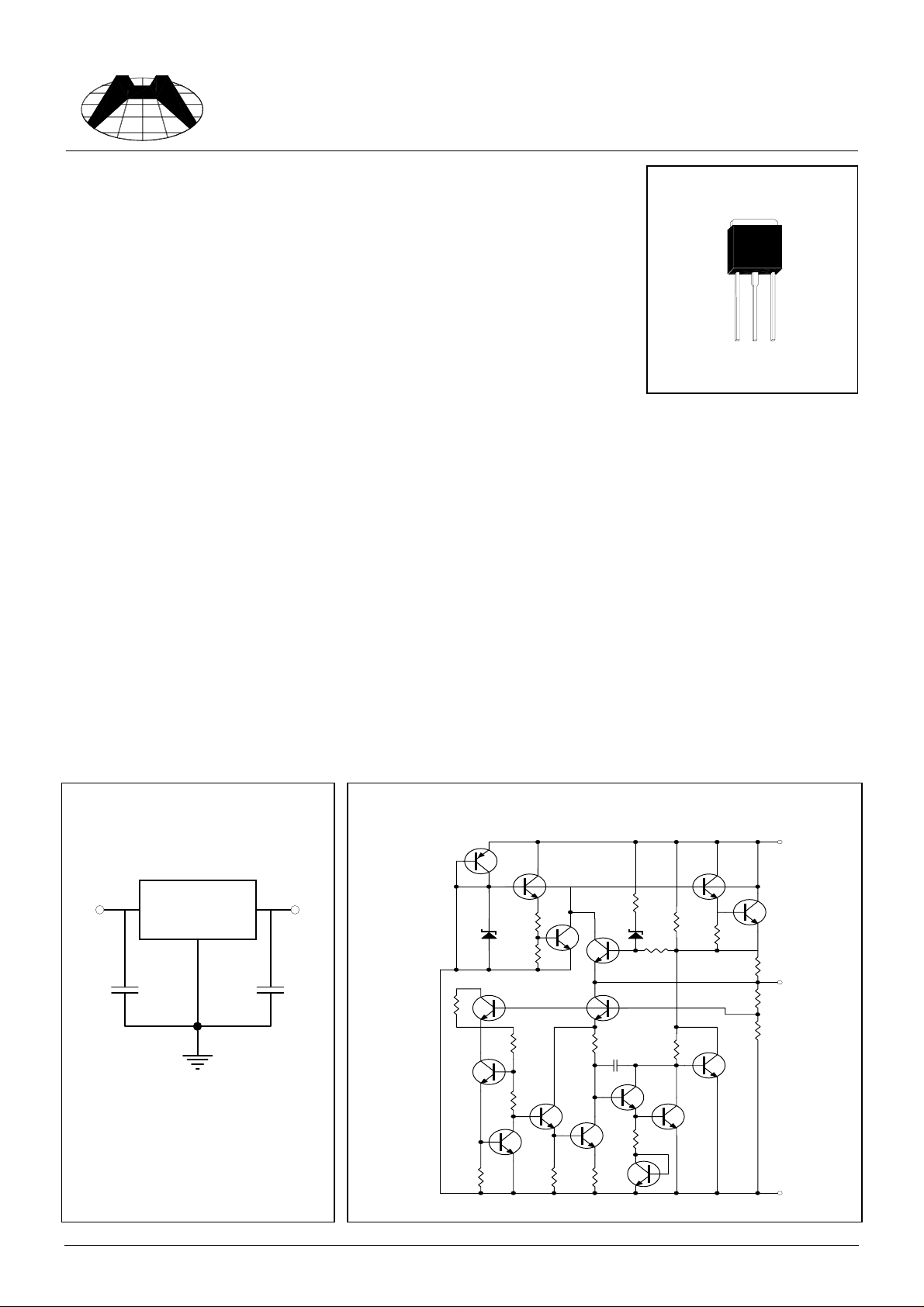
3-TERMINAL POSITIVE VOLTAGE REGULATOR
Description
The H7808_I series of three-terminal positive regulators are
available in the TO-251 package and with several fixed output
voltages, making it useful in a wide range of applications. These regulators can provide local
on-card regulation, eliminating the distribution problems associated with single point regulation.
Each type employs internal current limiting, thermal shut-down and safe operating area
protection, making it essent-ially indestructible. If adequate heat sinking is provided, they can
deliver over 1A output current. Although designed primarily as fixed voltage regulators, these
devices can be used with external components to obtain adjustable voltages and currents.
H7808_I is characterized for operation from 0°C to +125°C, and if operating temperature will always hi, please refer the power dissipation curve.
Absolute Maximum Ratings
Input Voltage......................................................................... 35 V (5V Through 9V), 40 V (24V)
•
Total Power Dissipation ........................................................................................... Internal limit
•
Operating Temperature Range............................................................................ 0 °C to +70 °C
•
Maximum Junction Temperature...................................................................................... 125 °C
•
Storage Temperature Range .......................................................................... -55 °C to +150 °C
•
Lead Temperature (Soldering 10S).................................................................................. 230 °C
•
(Ta=25°C)
Typical Application Schematic Diagram
Input
VoutVin
20pF
10K
1K
200
2K
0.3
Output
VREF
26
4K
H7808_I
C1 C2
6.3V
30K
3.4K
200
1.9K
Note :
C1 and C2 are requir ed if regulator
is located far from power supply
filter and load, or oscillation may
induced on the loop.
26
4K
1.2
12.1K
1K
HSMC Product Specification
GND
HI-SINCERITY
MICROELECTRONICS CORP.
Electrical Characteristics
Vin=14V, Io=500mA, 0°C≤Tj≤125°C (unless otherwise noted)
Spec. No. : Preliminary Data
Issued Date : 1998.08.01
Revised Date : 2000.10.01
Page No. : 2/3
Symbol Parameter Conditions
Vo Output Voltage
Tj=25°C
PD≤15W, 5mA≤Io≤1A
Vo
∆
Vo
∆
Line Regulation
Load Regulation
IQ Quiescent Current
IQ
∆
Quiescent Current
Change
Vn Output Noise Voltage
RR Ripple Rejection
VD Dropout Voltage
Isc Short Circuit Current
Ipk Peak Output Current
Vo / ∆T
∆
Average Tc of Vout
Tj=25°C, 10.5V≤Vin≤25V
Tj=25°C, 11.5V≤Vin≤17V
5mA≤Io≤1A
250mA≤Io≤750mA
Io≤1A, Tj=25°C
5mA≤Io≤1A
10.5V≤Vin≤25V
Ta=25°C, 10Hz≤f≤100KHz
11.5V≤Vin≤21.5V, f=120Hz
Tj=25°C, Io=1A
Tj=25°C
Tj=25°C
0°C≤Tj≤+125°C, Io=5mA
H7808AI
Min Typ Max
7.76 8 8.24
7.76 8 8.24
-580
-540
- - 100
--50
Units
V
mV
mV
-5.58 mA
--0.5
--1.3
mA
- - 200 uV
-68- dB
-2- V
-1.5- A
1.7 - - A
--0.8H7808BI
Min Typ Max
7.7 8 8.3
7.6 8 8.4
- 5 160
-280
- - 160
--80
mV/°C
Units
V
mV
mV
-5.58 mA
--0.5
--1.3
mA
- - 300 uV
62 73 - dB
-2.5- V
-1.5- A
1.7 - - A
--0.8-
mV/°C
HSMC Product Specification
 Loading...