

HSMC H603AL Datasheet
HI-SINCERITY
MICROELECTRONICS CORP.
Spec. No. : Preliminary Data
Issued Date : 1998.07.01
Revised Date : 1999.08.01
Page No. : 1/5
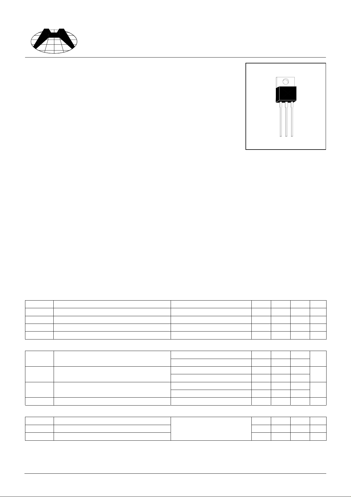
H603AL
N-Channel Logic Level Enhancement Mode Field Effect Transistor
Description
This very high density process has been especially tailored to minimize onstate resistance and provide superior switching performance. These
devices are particularly suited for low voltage applications such as DC/DC
converters and other battery powered circuits where fast switching, low inline power loss, and resistance to transients are needed.
(Ta=25°C)
Absolute Maximum Ratings
Maximum Temperatures
•
Operating and Storage Temperature................................................................................ -65 ~ +175 °C
Maximum Power Dissipation
•
Total Power Dissipation at Tc=25°C ............................................................................................... 60 W
Derate Above 25°C................................................................................................................ 0.4 W / °C
Maximum Voltages and Currents
•
Drain-Source Voltage...................................................................................................................... 30 V
Gate-Source Voltage -Continuous................................................................................................ ± 20 V
Drain Current -Continuous.............................................................................................................. 30 A
Drain Current -Pulsed................................................................................................................... 100 A
Thermal Resistance, Junction-to-Case .................................................................................. 2.5 °C / W
Thermal Resistance, Junction-to-Ambient............................................................................ 62.5 °C / W
Electrical Characteristics
Off Characteristics
•
Symbol Parameter Condition Min Typ Max Unit
BV
DSS
I
DSS
+I
GSS
-I
GSS
On Characteristics
•
V
GS(TH)
RDS(on) Static Drain-Source On-Resistance
IDS(on) On-State Drain Current
g
FS
Dynamic Characteristic
•
C
iss
C
oss
C
rss
Drain-Source Breakdown Voltage VGS=0V, ID=250uA 30 - - V
Zero Gate Voltage Drain Current VDS=30V, VGS=0V - - 10 uA
Gate-Body Leakage, Forward VGS=20V, VDS=0V - - 100 nA
Gate-Body Leakage, Reverse VGS=-20V, VDS=0V - - -100 nA
Gate Threshol d Vo ltage
V
DS=VGS
V
DS=VGS
, ID=250uA 1.1 - 3
, ID=10mA 1.4 - 3
VGS=10V, ID=25A - 0.018 0.022
V
=4.5V, ID=10A - 0.029 0.040
GS
VGS=10V, VDS=10V 60 - -
=4.5V, VDS=10V 15 - -
V
GS
Forward Transconductance VDS=10V, ID=25A - 26 - S
Input Capacitance - 1100 - pF
Output Capacitance - 600 - pF
Reverse Transfer Capacitance
V
=15V, VGS=0V
DS
f=1.0Mhz
- 180 - pF
V
Ω
A
HSMC Product Specification
HI-SINCERITY
V
MICROELECTRONICS CORP.
Switching Characteristics
•
Spec. No. : Preliminary Data
Issued Date : 1998.07.01
Revised Date : 1999.08.01
Page No. : 2/5
Symbol Parameter Condition Min Typ Max Unit
T(on)
T(off)
Q
g
Q
gs
Q
gd
Drain-Source Diode Characteristics And Maximum Ratings
•
V
SD
Turn-On Delay Time - - 30 ns
V
Turn -On Rise Time - - 110 ns
Turn-Off Delay Time - - 150 ns
Turn -Off Fa ll Time
Total Gate Charge - - 45 nC
Gate-Source Charge - - 10 nC
Gate-Drain Charge
Maximum Continuous Drain-Source Diode Forward Current
Drain-Source Diode Forward Voltage VGS=0V, IS=25A
=15V, ID=25A
DS
=10V, R
V
GS
=10V, ID=25A,
V
DS
=10V
V
GS
GEN
=24
Ω
- - 130 ns
- - 10 nC
--25A
--1.3V
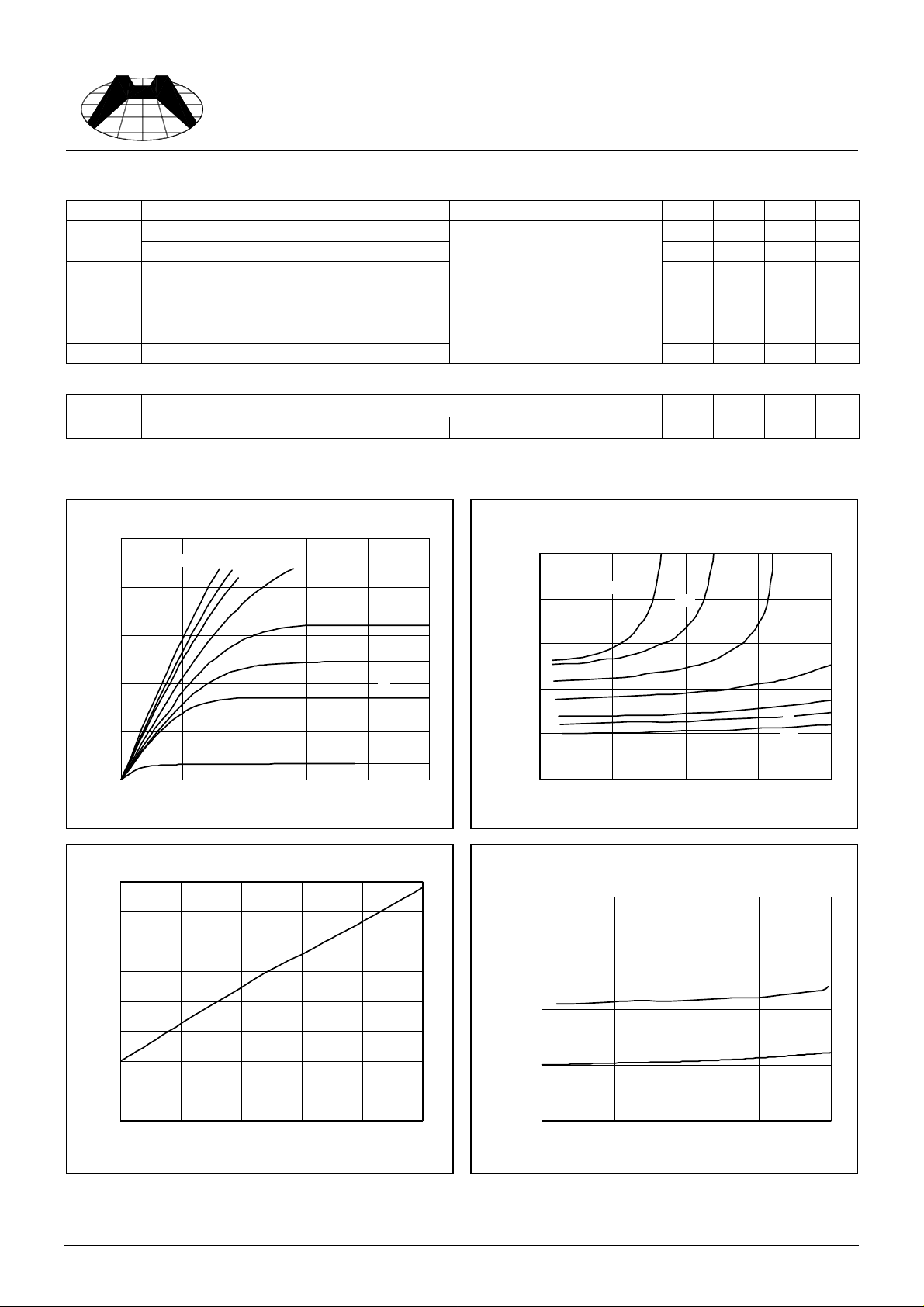
Characteristics Curve
100
VGS=10V
80
60
40
Drain-Source Current (A)
20
0
012345
8V
6V7V
Drain-Source Voltage (V)
5V
4.5V
4V
3V
On Resistance Variation & Temperature
1.6
1.5
On-Region C ha racteristic
1.4
1.3
1.2
1.1
1.0
0.9
Norm alize d Drain-Source O n-R esistan ce
ID=25A
VGS=10V
On-Resistance Variation With Gate Voltage &
3.0
2.5
2.0
Resistance
1.5
Norma liz e d Drain-So urce On-
1.0
0.5
0 20406080
Drai n Cur rent
VGS= 4V
4.5V
5 V
6V
7V
8V
10
Drain Curre nt (A)
On-Resistance Variation & Drain Current &
2.5
VGS=10V
2
1.5
Resistance
1
Norma liz e d Drain-So urce On-
Temperature
TJ=125°C
TJ=25°C
0.8
25 50 75 100 125 150
Junction Temperature (°C)
0.5
020406080
Drain Curre nt (A)
HSMC Product Specification
 Loading...