

HSMC H431CM, H431BM, H431AM Datasheet
HI-SINCERITY
MICROELECTRONICS CORP.
Spec. No. : Preliminary Data
Issued Date : 1998.04.08
Revised Date : 2001.02.15
Page No. : 1/4
H431AM/BM/CM
AJDUSTABLE SHUNT REGULATOR
Description
The H431XM series are three-terminal adjustable regulators with guaranteed thermal stability over applicable temperature ranges. The
output voltage may be set to any value between V
2.495 volts) and 36 volts with two external resistors. These devices
have a typical dynamic output impedance of 0.2Ω. Active output
circuitry provides a very sharp turn-on characteristic, making these devices excellent replacement for zener diodes in many applications.
Features
Programmable output voltage
•
Temperature coefficient is 50ppm/°C typical
•
Temperature compensated for operation ov er
•
full temperature range
•
Low output noise voltage
•
Fast turn on response
•
(approximately
REF
Classification
Rank A B C
V
REF
2.495±2% 2.495±1% 2.495±0.5%
Absolute Maximum Ratings
( Operating temperature range applies unless otherwise specified )
Characteristics Symbol Value Unit
Cathode Voltage V
Cathode Current Range (Continuous) I
Reference Input Current Range I
Power Dissipation P
Operating Temperature Rang e T
Storage Temperature Range T
KA
K
REF
D
opr
stg
-100~+150 mA
0.05~+10 mA
-65~+150
37 V
770 mW
0~+70
C
°
C
°
H431AM, H431BM, H431CM HSMC Product Specification
HI-SINCERITY
)
)
MICROELECTRONICS CORP.
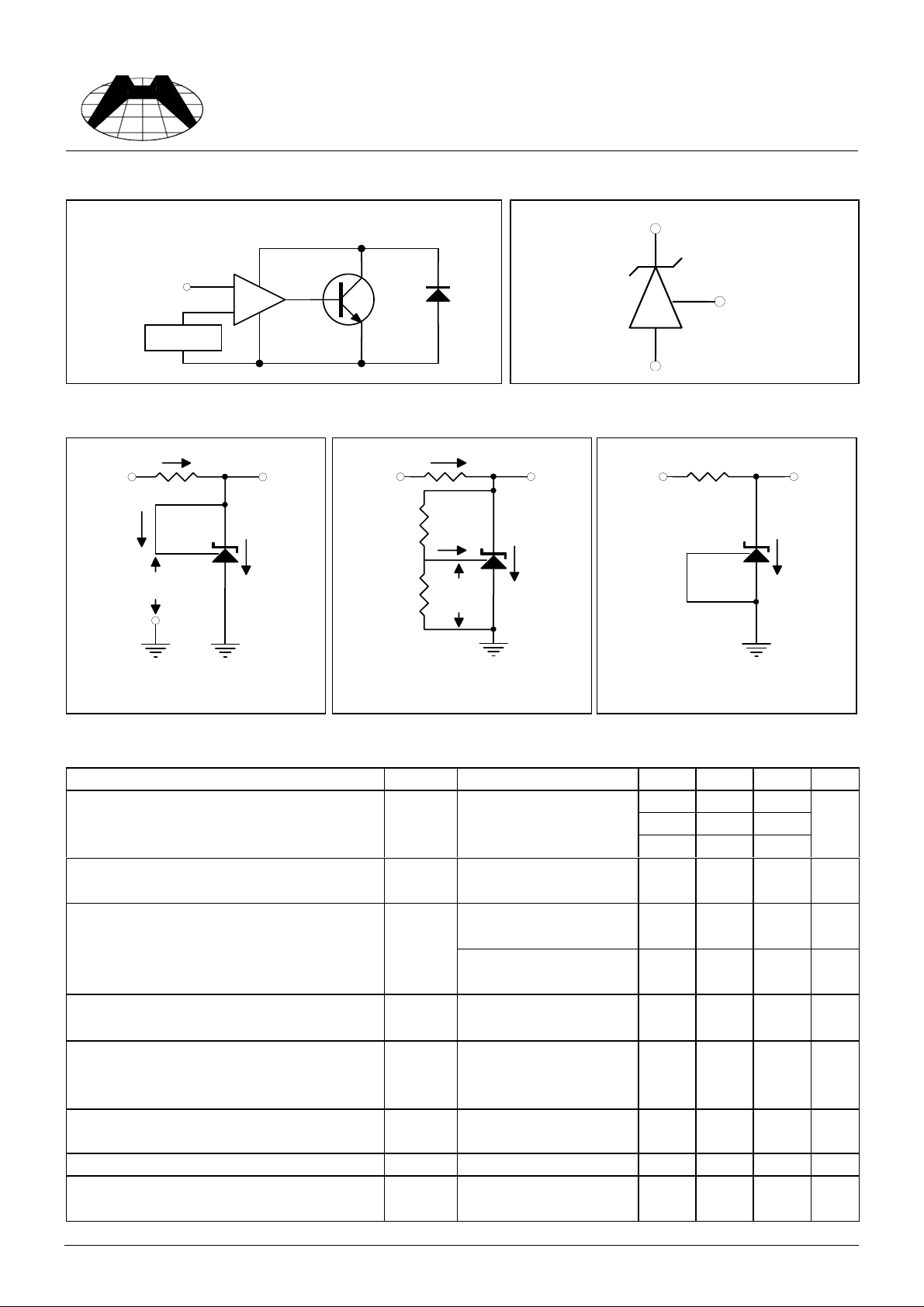
Functional Block Diagram & Symbol
Spec. No. : Preliminary Data
Issued Date : 1998.04.08
Revised Date : 2001.02.15
Page No. : 2/4
Functional Block Diagram : Symbol :
Cathode
Reference
+
-
V
REF
Anode
Test Circuits
IN
I
REF
V
I
I
REF
V
Z
I
Z
IN
I
I
I
REF
V
REF
V
Z
I
Z
Cathode
Reference
Anode
IN V
Z
Fig1. Test Circuit for VZ=V
Electrical Characteristics
REF
Fig 2. Test Circuit for VZ>V
Note : VZ=V
( Ta=25°C unless otherwise specified )
Characteristics Symbol Test Conditions Min Typ Max Unit
Reference Input Voltage
H431AM 2.445 2.495 2.545
H431BM 2.470 2.495 2.520
H431CM
Deviation of Reference Input Voltage
Over-Temperature
Ratio of Change in Reference Input
Voltage to the Change in Cathode
V
∆
Voltage
Reference Input Current I
Deviation of Reference Input Current
Over Full Temperature Range
I
Minimum Cathode Current for
Regulation
Off-State Cathode Current I
Dynamic impedance Z
REF
V
REF
REF(dev
V
REF
V
∆
KA
REF
REF(dev
I
K(min)
K(off)
KA
REF
REF
REF
T
≤
a
REFxR1
, IK=10mA
, IK=10mA
T
≤
max
(1+R1/R2)+I
VKA=V
VKA=V
T
min
IK=10mA,
VKA=10V-V
∆
/
REF
IK=10mA,
KKA=36V-10V
∆
IK=10mA, R1=10kΩ,
R2=
∞
IK=10mA, R1=10kΩ,
R2=∞, Ta=Full
Range
VKA=V
VKA=36V, V
VKA=V
REF
REF
, f≤1.0KHz
REF
IK=1 to 100mA
Fig3. Test Circuit for Off-State
Current
V
2.480 2.495 2.510
-417mV
--1.4-2.7mV
--1.0-2.0V
-24uA
-0.41.2uA
-0.41.0mA
=0 - 0.1 1.0 uA
-0.20.5
Ω
H431AM, H431BM, H431CM HSMC Product Specification
 Loading...