

HSMC H431CA, H431BA, H431AA Datasheet
HI-SINCERITY
MICROELECTRONICS CORP.
Spec. No. : HA200216
Issued Date : 1998.04.08
Revised Date : 2002.08.27
Page No. : 1/4
H431AA/BA/CA
AJDUSTABLE SHUNT REGULATOR
Description
The H431 series are three-terminal adjustable regulators with guaranteed thermal stability over applicable temperature ranges. The output voltage may be set to any value between VREF (approximately
2.495 volts) and 36 volts with two external resistors. These devices
have a typical dynamic output impedance of 0.2Ω. Active output circuitry provides a very sharp turn-o n ch aracteristic, maki ng these dev ices excell ent replac ement for
zener diodes in many applications.
Features
• Programmable output voltage
• Temperature coefficient is 50ppm/°C typical
• Temperature compensated for operation over
• full temperature range
• Low output noise voltage
• Fast turn on response
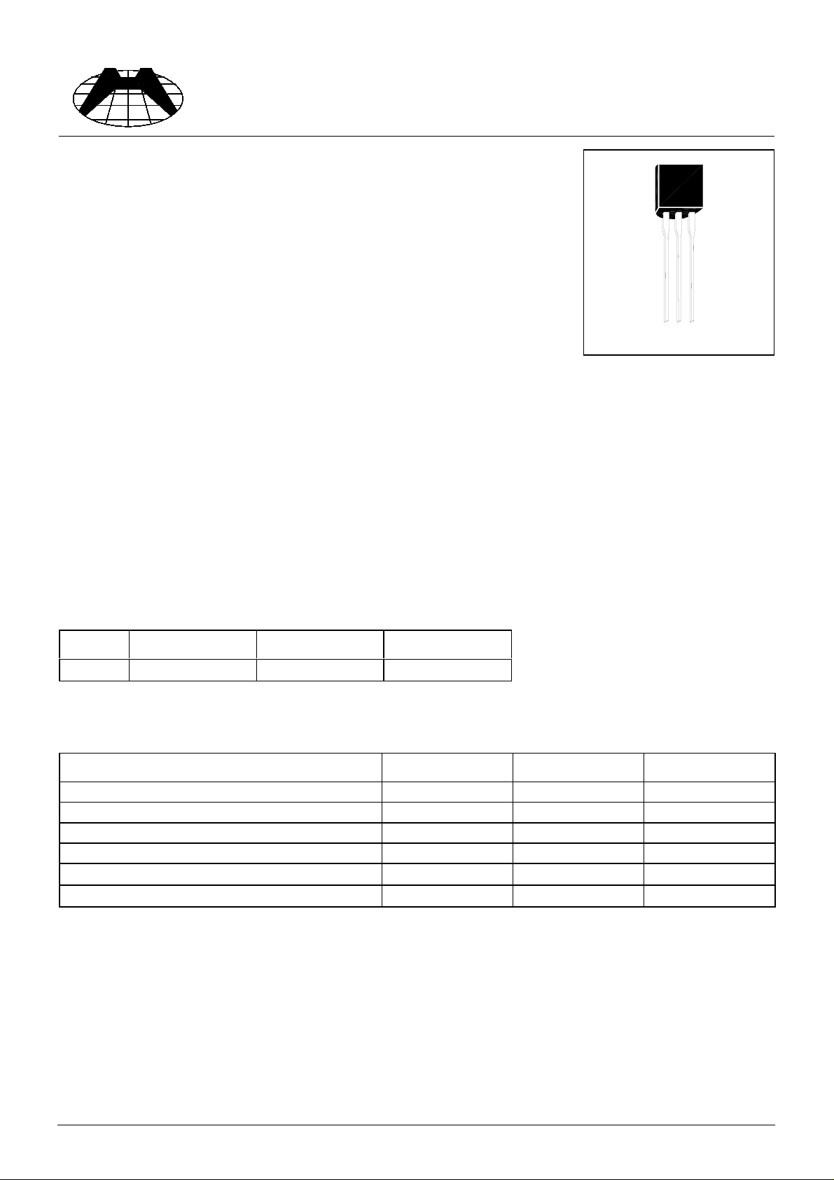
TO-92
Classification
Rank A B C
VREF
2.495±2% 2.495±1% 2.495±0.5%
Absolute Maximum Ratings
(Operating temperature range applies unless otherwise specified)
Characteristics Symbol Value Unit
Cathode Voltage V
Cathode Current Range (Continuous) I
Reference Input Current Range I
Power Dissipation P
Operating Temperat ur e Range T
Storage Temperatur e Range T
KA
K
REF
D
opr
stg
37 V
-100~+150 mA
0.05~+10 mA
770 mW
0~+70
-65~+150
°C
°C
H431AA, H431BA, H431CA HSMC Product Specification
HI-SINCERITY
)
)
A
A
MICROELECTRONICS CORP.
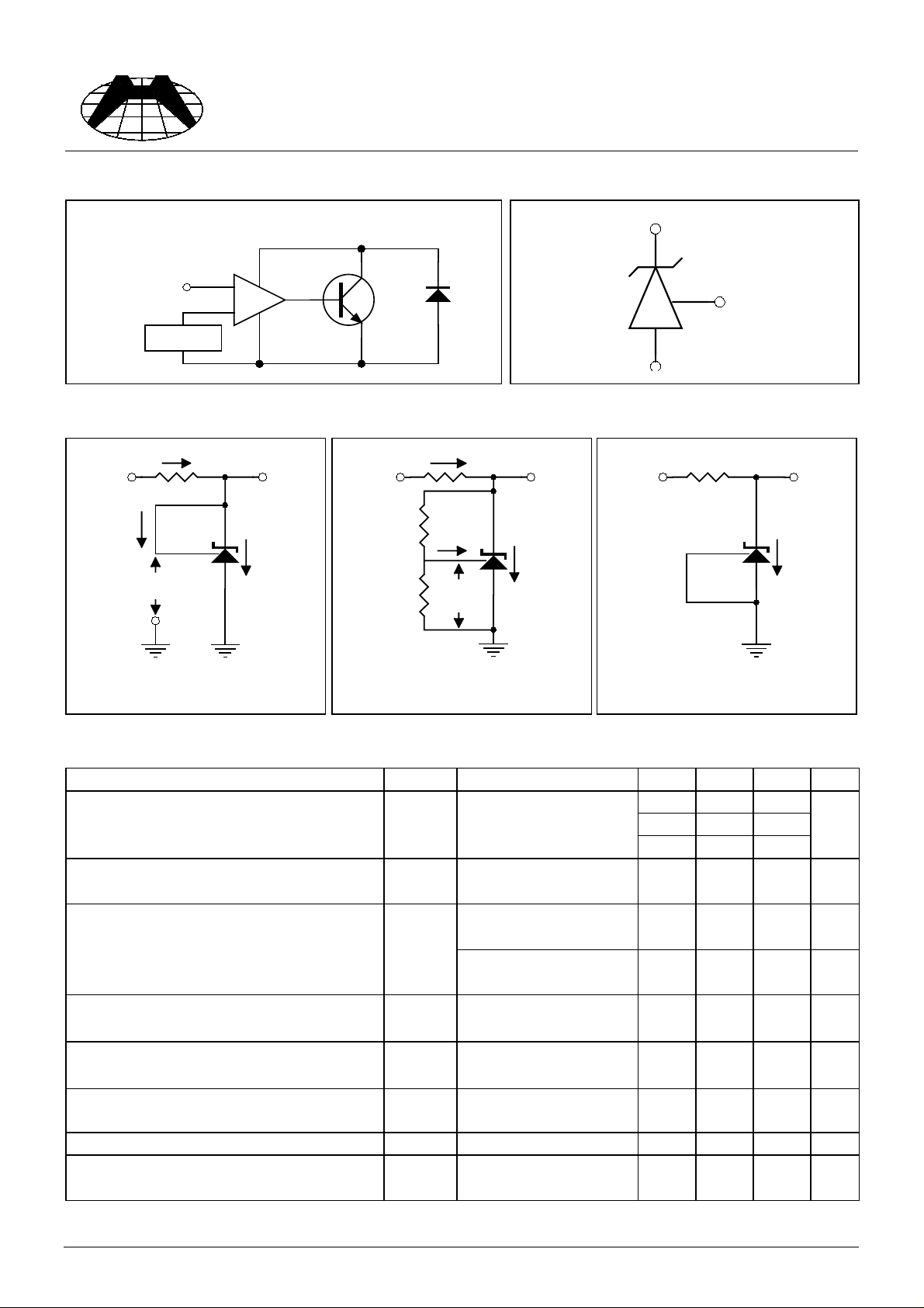
Functional Block Diagram & Symbol
Spec. No. : HA200216
Issued Date : 1998.04.08
Revised Date : 2002.08.27
Page No. : 2/4
Functional Block Diagram : Symbol :
Cathode
Reference
+
-
V
REF
node
Test Circuits
IN
IREF
II
VREF
IZ
Z
V
IN
II
VZ
REF
I
IZ
VREF
IN
Cathode
node
Reference
V
Z
Fig1. Test Circuit for VZ=VREF
Electrical Characteristics
Fig 2. Test Circuit for VZ>VREF
Note : VZ=VREF(1+R1/R2)+IREFxR1
( Ta=25°C unless otherwise specified )
Characteristics Symbol Test Conditions Min Typ Max Unit
Reference Input Voltage
H431AA 2.445 2.495 2.545
H431BA 2.470 2.495 2.520
H431CA
Deviation of Reference Input Voltage
Over-Temperature
V
Ratio of Change in Reference Input
Voltage to the Change in Cathode
Voltage
Reference Input Current I
Deviation of Reference Input Current
Over Full Temperature Range
Minimum Cathode Current for
Regulation
Off-State Cathode Current I
Dynamic impedance Z
V
REF
REF(dev
∆V
REF
∆V
REF
I
REF(dev
I
K(min)
K(off)
VKA=V
VKA=V
T
REF
REF
min≤Ta≤Tmax
IK=10mA,
∆VKA=10V-V
/
IK=10mA,
KA
∆KKA=36V-10V
IK=10mA, R1=10kΩ,
R2=∞
IK=10mA, R1=10kΩ,
R2=∞, Ta=Full Range
VKA=V
REF
VKA=36V, V
VKA=V
KA
IK=1 to 100mA
REF
Fig3. Test Circuit for Off-State
Current
, IK=10mA
2.480 2.495 2.510
, IK=10mA
-417mV
- -1.4 -2.7 mV
REF
- -1.0 -2.0 V
-24uA
-0.41.2uA
-0.41.0mA
=0 - 0.1 1.0 uA
REF
, f≤1.0KHz
-0.20.5
V
Ω
H431AA, H431BA, H431CA HSMC Product Specification
 Loading...