

HSMC H393P Datasheet
HI-SINCERITY
MICROELECTRONICS CORP.
Spec. No. : Preliminary Data
Issued Date : 2001.05.01
Revised Date : 2001.06.22
Page No. : 1/3
H393P
LOW POWER L OW OFFSET VOLTAGE COMPARATORS
Description
The H393P series consists of two independent precision voltage
comparators designed specifically to operate from a single power supply
over a wide range of voltages, the input common mode voltage range
includes ground. Owing to adoption of clamp circuitry in input pins, misoperation is prevented by negative input.
Features
Wide power supply voltage range
•
Single power supply.............................................................................................................. 2 V to 30 V
Dual power supplies........................................................................................................ ± 1 V to ± 15 V
Wide input common-mode voltage range.................................................................... 0 V to (Vcc-1.5) V
•
Low input bias current............................................................................................................. 25 nA typ.
•
High sink current capability because of open collector otput 40mA min.
•
Pin Configurations
5678
-
+
+
-
4321
Equivalent Circuit
-IN
1K
Pin 1 : Output A Pin 5 : + Input B
Pin 2 : - Input A Pin 6 : - Input B
Pin 3 : + Input A Pin 7 : Output B
Pin 4 : GND Pin 8 : Vcc
Vcc
OUT
+IN
H393P HSMC Product Specification
1K
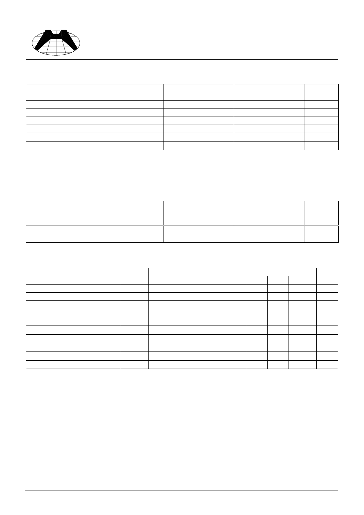
HI-SINCERITY
(+)
(-)
MICROELECTRONICS CORP.
Spec. No. : Preliminary Data
Issued Date : 2001.05.01
Revised Date : 2001.06.22
Page No. : 2/3
Absolute Maximum Ratings
(see Note)
Rating Symbol Value Unit
Power Supply Voltage VCC 36 V
Differential Input Voltage VID 36 V
Common-Mode Input Voltage VI -5 to 36 V
Output Short Current to GND - Infinite* Power Dissipation PD
350 (Ta≤55°C)
Operating Temperature Ta -20 to +75
Storage Temperature Tstg -55 to +125
*: This value is specified with respect to the short circuit from output to GND. However, short circuit from the output to VCC
cause device destruction.
Note: Permanent device damage may occur if the above Absolute Maximum Ratings are exceeded. Functional operation should
be restricted to the conditions as detailed in the operational sections of this data sheet. Exposure to absolute maximum
rating conditions for extended periods may affect device reliability.
mW
C
°
C
°
Recommended Operating Conditions
Rating Symbol Value Unit
Power Supply Voltage VCC
Operating Temperature Ta -20 to +75
Output Sink Current Isink
2 to 30
1.0 to ±15
±
40
≤
V
C
°
mA
Electrical Characteristics
Parameter Symbol Conditions
(Vcc=5V, Ta=25°C)
Value
Min Typ Max
Units
Input Offset Voltage Vio Vo=VREF=1.4V - 2 5 mV
Input Offset Current Iio - - 5 50 nA
Input Bias Current Iin*1 - - 25 250 nA
Common-Mode Input Voltage Vcm*2 - 0 - Vcc-1.5 V
Power Supply Current Icc
Voltage Gain Av
Response Time Output Sink Current Isink
Output Saturation Voltage Vol
Output Leakage Current Ileak Vin
Notes:
*1: Iin is measued when Vi≥0 and direction of the input current flows from IC. When negative voltage is applied to input pin, the
pin is equivalently connected the GND through a 1kΩ of resistor.
When low voltage below than –5V is applied, please connect a resistor serially to input pin in order to prevent the high
current flow.
*2: Positive input voltage may exceed the power supply voltage. As long as the other voltage remains in the common-mode
input voltage range, the comparator will provide a proper output state.
When Vcc=5V, your are requested to use Vin below 25V.
RL=
∞
RL=15kΩ, Vcc=15V
RL=1k
Vin
Vin
Ω
=0, Vin
(+)
=0, Vin
=1V, Vin
(+)
=1V, Vol≤1.5V
(-)
=1V, Isink≤30mA
=0, Vo=30V - - 1 uA
(-)
-2 3mA
- 200 - V/mV
-2 -us
40 - - mA
-0.20.4 V
H393P HSMC Product Specification
 Loading...