

HSMC H1563S, H1563P Datasheet
HI-SINCERITY
MICROELECTRONICS CORP.
Spec. No. : HP200201
Issued Date : 2000.10.01
Revised Date : 2002.07.12
Page No. : 1/8
HS200207
H1563P / H1563S
HIGH-EFFICIENCY DC/DC CONVERTER
Description
The H1563 is a monolithic control circuit containing the primary functions required for DC to DC converters
and highside-sensed constant current source. The device consists of an internal temperature compensated reference, comparator, controlled duty cycle oscillator with an active current sense circuit, bootstrapped driver, and high current output switch. This device is specifically designed to construct a constant
current source for battery chargers with a minimum number of external components. Bootstrapped driver
can drive the NPN output switch to saturation for higher eff-iciency and less heat dissipation. The H1563
can deliver 1.5A continuous current without requiring a heat sink.
Features
• 3V to 40V Input Voltage Operation
• Internal 2A Peak Current Switch
• 1.5A Continuous Output Current
• Bootstrapped Driver
• High Side Current Sense Capability
• High Efficiency (up to 90%)
• Internal ±2% Reference
• Low Quiescent Current at 1.6mA
• Frequency Operation from 100Hz to 100KHz
Applications
• Constant Current Source for Battery Chargers
• Saver for Cellular Phone
• Step-Down DC-DC Converter Module
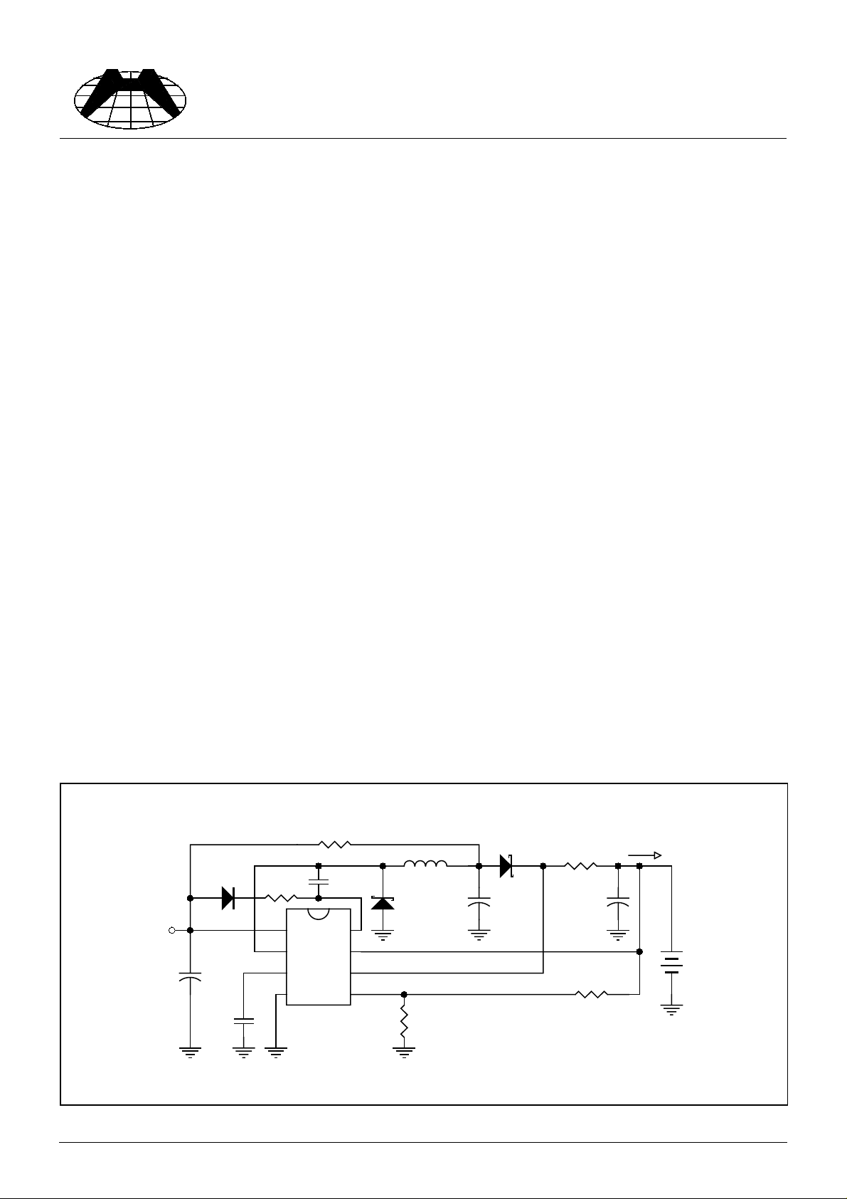
T y pical Application Circuit
Saver Circuit for Cellular Phone
R1
1K
Vin
+
D2
H1N4148
C1
220uF
CT
470pF
R2
120
C3
1uF
SC BST
SE IS
TC VCC
GND FB
H1563
L
220uH
D1
H1N5821
RA
5.6K
D3
H1N5819
+ +
Co
220uF
*RS
C5
10uF
RB
33K
Io
*Io=300mV/RS
H1563P / H1563S HSMC Product Specification
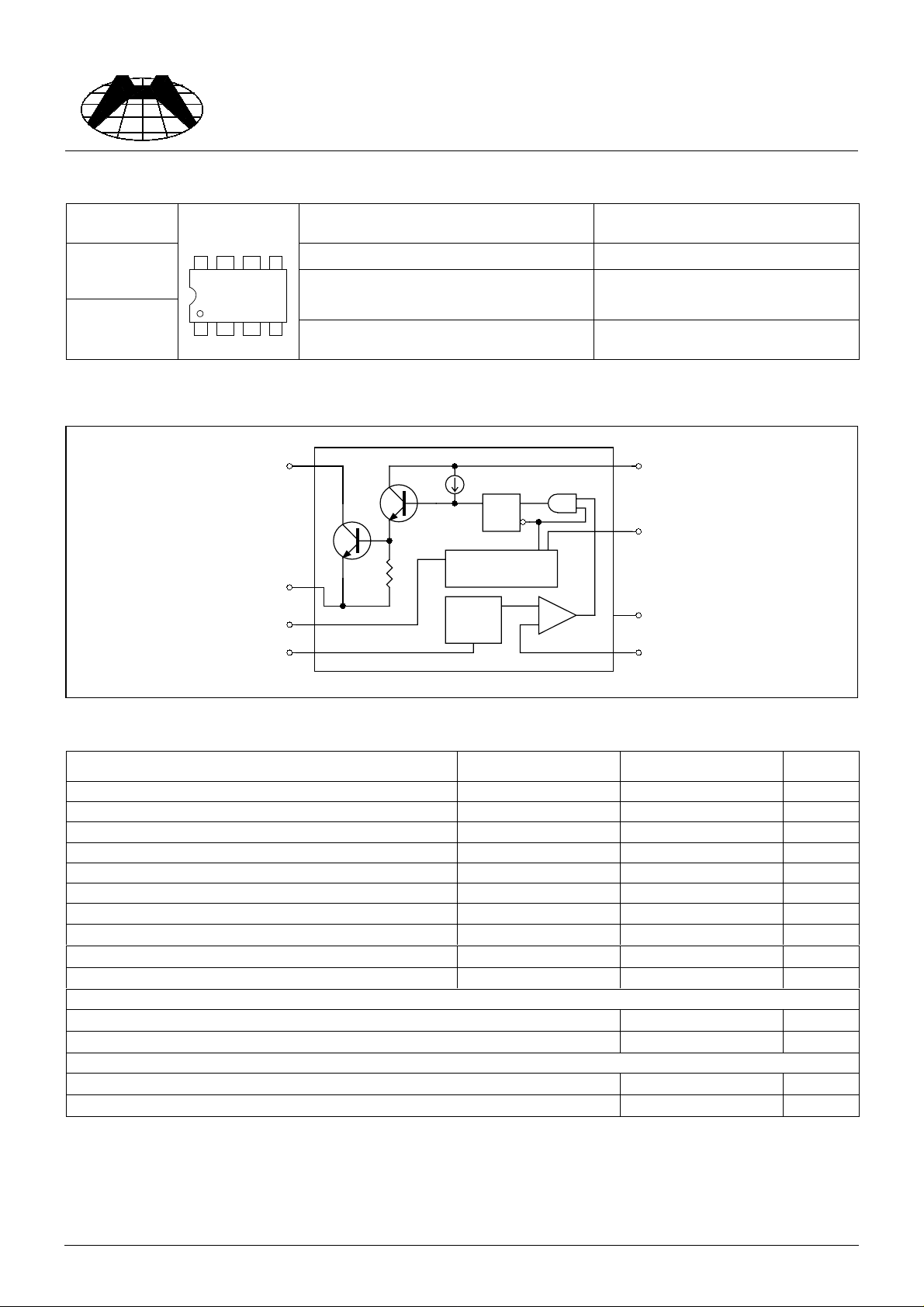
Pin Connections
HI-SINCERITY
MICROELECTRONICS CORP.
Spec. No. : HP200201
HS200207
Issued Date : 2000.10.01
Revised Date : 2002.07.12
Page No. : 2/8
Order No. Pin1: SC-2A Switch Collector
H1563P
Top View
Pin2: SE-Darlington Switch Emitter Pin6: VCC-Power Supply Input
5678
(Plastic DIP)
Pin3: TC-Oscillator Timing Capacitor
H1563S
(Plastic SO)
4321
Pin4: GND-Power Ground
Block Diagram
1
SC
Q2
CT Is
Oscillator
1.25V
Reference
Voltage
SE
TC
Q1
2
3
4
80
Pin5: FB-Feedback Comparator
Inverting Input
Pin7: IS-Highside Current Sense
Input
Pin8: BST-Bootstrapped Driver
Collector
8
BST
S
Q
R
+
Comparator
7
IS
6
VCC
5
FBGND
Absolute Maxium Rating
Rating Symbol Value Unit
Power Supply Voltage Vcc 40 Vdc
Comparator Input Voltage Range Vir 0.3 ~ +40 Vdc
Switch Collector Voltage Vc(switch) 40 Vdc
Switch Emitter Voltage (Vpin1=40V) Ve(switch) 40 Vdc
Switch Collector to Emitter Voltage Vce(switch) 40 Vdc
Driver Collector Voltage Vc(driver) 40 Vdc
Switch Current Isw 2 A
Operating Junction Temperature Tj 150
Operating Ambient Temperature Range Ta 0 to +70
Storage Temperature Range Tstg -65 to +150
DIP Package Power Dissipation and Thermal Characteristics:
Ta=25°C
Thermal Resistance 85
SO Package Power Dissipation and Thermal Characteristics:
Ta=25°C
Thermal Resistance 105
1.5 W
°C/W
1.2 W
°C/W
°C
°C
°C
H1563P / H1563S HSMC Product Specification
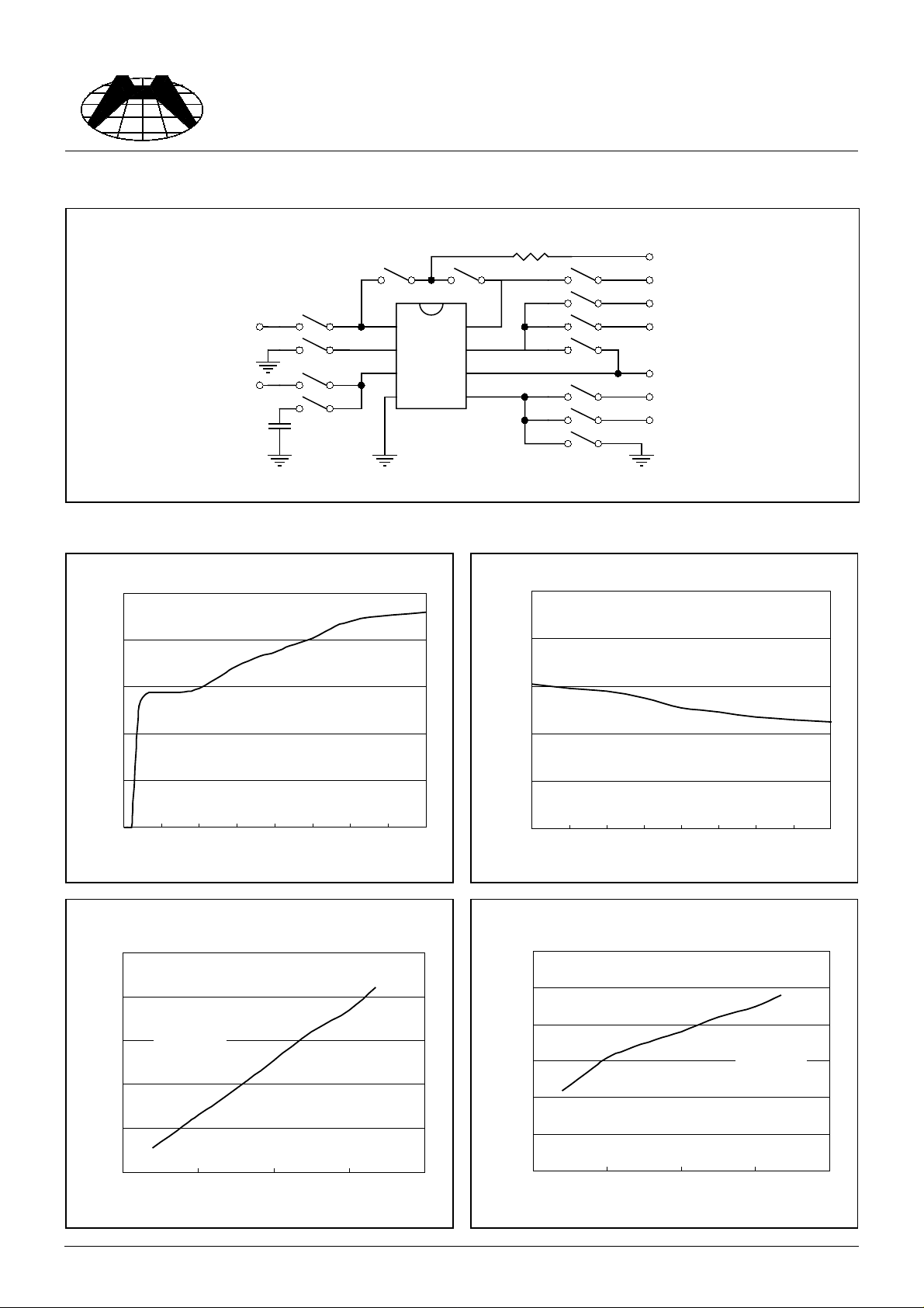
Test Circuit
HI-SINCERITY
MICROELECTRONICS CORP.
Spec. No. : HP200201
HS200207
Issued Date : 2000.10.01
Revised Date : 2002.07.12
Page No. : 3/8
Current Source
I
1A
2V/0V
DISCHG/ICHG
CT
1nF
Characteristics Curve
Standby Supply Current vs Supply Voltage
2
1.6
1.2
1
SC BST
2
SE IS
3
TC VCC
4
GND FB
H1563
R1
1K
8
7
6
5
VCC
20mA
Current Source
4.55V
@VCC=5V
4.75V
VCC
1.275V
1.225V
Vfb Theshol d Vol t age vs Temper ature
1.3
1.28
1.26
0.8
Icc Supply Cur rent (m A)
0.4
0
0 5 10 15 20 25 30 35 40
Vcc Suppl y Voltage (V)
Common Emitter Configuration Output Switch
Saturation Voltage vs Collector Current
1
0.8
0.6
0.4
Vce(sat) Saturation Voltage (V)
0.2
VCC=5V
PIN7=VCC
PIN 2,3,5=GND
Forced Beta=20
0
00.511.52
Ic Coll e c tor Current ( A )
1.24
Vfb Thresh ol d Voltage (V)
1.22
1.2
0 1020304050607080
Temperatu re (J)
VCC=5V
Ct=1nF
PIN2=GND
Emmiter Follower Configuration Output Switch
Saturtion Voltage vs Emmiter Current
1.8
1.7
1.6
1.5
1.4
Vce(sat) Sar urtion Vol tage ( V)
1.3
1.2
00.511.52
Ie Emitter (A)
VCC=5V
PIN1,7 ,8=VCC
PIN3,5=GND
H1563P / H1563S HSMC Product Specification
 Loading...