


HPC model Service Manual
Factory Model : 17”19”LCD MONITOR
TABLE OF CONTENTS
I. SAFETY PRECAUTIONS
II.PRODUCT SAFETY NOTICE
III.SERVICE NOTES
V. SERVICE TOOL & EQUIPMENT REQUIRED
VI. SPECIFICATIONS
VII.LCD MONITOR BLOCK DIAGRAM
VIII.TROUBLE SHOOTING FLOW CHART
IX . LCD MONITOR ADJUSTMENT
X. USER SAFETY NOTICE
HPC electronic(shenzhen)co.,LTD
January 2007
1

I.SAFETY PRECAUTIONS
This monitor is manufactured and tested on a ground principle that a user's safety comes first. However, improper use or
installation may cause damage to the monitor as well as to the user. Carefully go over the following WARNINGS before
installing and keep this guide handy.
WARNINGS:
1. This monitor should be operated only at the correct power sources indicated on the label on the rear end of the monitor. If
you're unsure of the power supply in your residence, consult your local dealer or power company.
2. Use only the special power adapter that comes with this monitor for power input.
3.Do not try to repair the monitor yourself, as it contains no user-serviceable parts. Only a qualified technician should repair
this monitor.
4.Do not remove the monitor cabinet. There are high-voltage parts inside that may cause electric shock to human bodies,
even when the power cord is unplugged.
5.Stop using the monitor if the cabinet is damaged. Have it checked by a service technician.
6 Put your monitor only in a clean, dry environment. If it gets wet, unplug the power cable immediately and consult your
service technician.
7.Always unplug the monitor before cleaning it. Clean the cabinet with a clean, dry cloth. Apply non-ammonia based cleaner
onto the cloth, not directly onto the glass screen.
8.Do not place heavy objects on the monitor or power cord.
II. PRODUCT SAFETY NOTICE
Many electrical and mechanical parts in this chassis have special safety visual inspections and the protection afforded by them
cannot necessarily be obtained by using replacement components rated for higher voltages, wattage, etc. Before replacing any
of these components read the parts list in this manual carefully. The use of substitute replacement parts that do not have the
same safety characteristics as specified in the parts list may create shock, fire, or other hazards.
III.SERVICE NOTES
1. When replacing parts or circuit boards, clamp the lead wires around terminals before soldering.
2. When replacing a high wattage resistor (more than 1W of metal oxide film resistor) in circuit board, keep the resistor
about 5mm away from circuit board.
3. Keep wires away from high voltage, high temperature components and sharp edges.
4. Keep wires in their original position so as to reduce interference.
5. Usage of this product please refers to also user's manual.
V. SERVICE TOOL & EQUIPMENT REQUIRED
1. SIGNAL GENERATOR OR PC
2. SCREW DRIVER
3. IRON
4. ABSORBER
5. SOLDER
VI.SPECIFICATIONS
5.1 PRODUCT SPECIFICATIONS
LCD panel 17’’/19" TFT
2
Power management Energy Star compliant VESA
DPMS compatible
Displayable Resolution 1024 x 1280 75Hz (max.)
Pixel Dimension 0.264 (V) x 0.264 (H) mm /0.296(H) / 0.296(V) mm
LCD Display Color 8bit
Viewing Angle Horizontal: ± 80
Contrast Ratio 500 : 1
Brightness 300 cd/m2
Response Time 12ms
Active Display Area 337.920 (H) x 270.336(V) /376.32mm x 301.056mm
Temperature Operating 0°C ~ +35°C
Storage -20°C ~ +60°C
Compliance CE, FCC ,CB,CCC
Power Input Voltage AC 110-240V
Consumption 40w(max)
Audio 2w(L) + 1(R)
5.2 SUPPORTING TIMING CHART(timing chart)
o
H Vertical: ±80o V
MODE
L
support frequency
H-
ynnc(K
bandwidth
(MHZ)
Signal polarity
H V
HZ)
1 VGA 640 X 480 60Hz 31.47 25.175 - +
2 VESA 640 X480 72Hz 37.86 31.5 - +
3 VESA 640 X 480 75Hz 37.5 31.5 - +
4 VGA 720 X 400 70HZ 31.47 28.322 - +
5 VESA 800 X 600 60Hz 37.88 40 + +
6 VESA 800 X 600 72Hz 48.08 50 + +
7 VESA 800 X 600 75Hz 46.88 49.5 + +
8 MAC 832 X 624 75Hz 49.72 57.28 - +
9 VESA 1024 X 768 60Hz 48.36 65 - -
10 VESA 1024 X 768 70Hz 56.48 75 - -
11 VESA 1024 X 768 75Hz 60.02 78.75 + +
12 MAC1152X 870 75Hz 68.68 100 - -
13 VESA1280X1024 60Hz 60 108 + +
14 VESA1280 X 1024 75Hz 80 135 + +
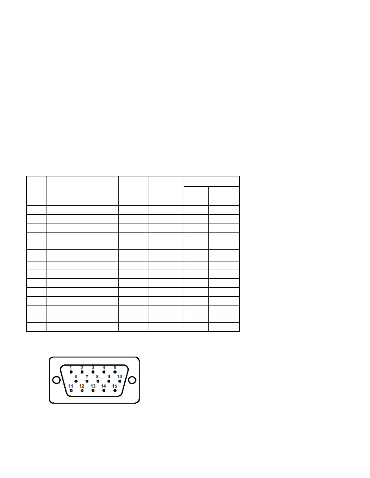
5.3 Pin - Assignment of 15-pin D-sub:
CONNECTOR SIGNAL DESCRIPTION
1.RED 2.GREEN 3.BLUE 4.NC 5.GND
6.GND 7.GND 8.GND 9. NC 10.GND
3
11.NC 12.SDA 13.H.hync 14.V.hync 15.SCL
Check on/Off
Replacing AC Power
Check
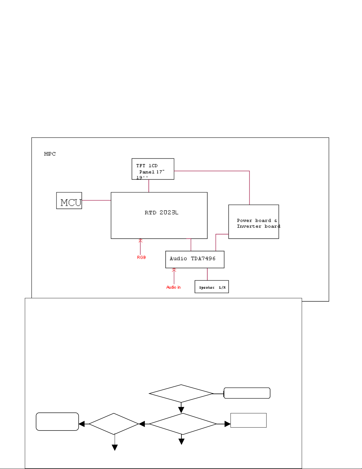
VII: BLOCK DIAGRAM
VIII:TROUBLE SHOOTING FLOW CHART
7.1 No power.
Check peripheral
electrocircuit
NG
OK
Cn6 pin1 12V
OK
OK
NG
Check U2 mcu
touch area.
4

Check Y1
Check U2 on
3.3V
Check cn3
Rework cn10 to panel
Check Pcsignaland
others.
NG
OK
Replacing
ok
NG
Panel
7.2 No display
Check component on inverter
board.
NG
Replacing inverter
NG
Check power supply
NG
Check electrocircuit
OK
Replacing RTD2023Lor
Check cn6 5V For panel
OK
Check cn1 connectoru
OK
OK
Replacing scaler IC
Checkcn6 pin1 12v
NG
Rework the connecter
NG
Check circuitry
7.3 loss color .
NG
OK
Check R/G/B signal input
Check PC signal R/G/B
5

7.4 NO AUDIO
Open volume in
OSD,
OK
Check 12V on
U8
pin15/pin16,and
5.5v on pin14/17
Check .signal wave
NG
Check CN8
connector
OK
NG
Check pc audio
input
ok
NG
Replacing
TDA7496L
IX.Adjustment
8.1 Adjustment Conditions and Precautions:
1.1.. Power supply voltage:
OK
Replacin
g
speaker
6

AC 110/120V± 10% 60 Hz± 5%, AC 220/240V± 10% 50 Hz ± 5%.
1.2 Warm up time:
The display must be power ON for at least 30 minutes at full white pattern before starting alignments. This is especially
critical in color temperature and white balance adjustments.
1.3signal input
reference the front detail specifications and timing table.
8.2Adjustment procedure
2.1. Timing : 1280x1024@75Hz.
2.2 Pattern : Full white.
2.3 Set Chroma Color analyzer at the center of screen and along a perpendicular to the screen at 20cm from the display.
2.4. Under the normal display model ,press “Down” to close your monitor, then press Up to open it ,monitor will be into
factory preset mode, and pull out signal cable, will be BURN in mode.
2.5 .Select “9300” menu, adjust “red” until x=281±30, adjust “blue” until y=311±30. Then exit “9300” menu.
2.6 Select “6500” menu, adjust “red” until x=313±30, adjust “blue” until y=329±30. Then exit “6500” menu.
2.7 DC ON/OFF again, monitor will be exit factory mode menu.
2.8.On the OSD menu, color temperature set to 6500.
2.9. Change each mode on the timing table in turns and execute the “Auto Adjust ” function, then all the data of the each mode
will be auto saved after finish the “Auto Adjust “ function.
X. Notice
9.1 I feel very thankful for buying our LCD products,and you can regard our repairing rules as your reference ;if we have
changed our repairing rules ,you will not be told again .Also, the eaxt repairing regulations should be in accordance with the
attched materials (include the product spcfication and use regulation)
9.2 The monitor has no any repairing material ,if you want to get service,please get in touch with local
agent, or dail our free telephone: 800-830-7242
9.3 The ultimate explanation right of the repairing spcefication should be owed by the R&D Center of Hui
Pu Electronics (Shen Zhen) Co.Ltd .
HPC electronic(shenzhen)co.,LTD
January 2007
7

A
B
C
D
E
RTD_3.3DVCC
PH2.0_8A
CN1
1
1
4 4
3
3
5
5
7
7
9
9
10
2
2
4
4
6
6
8
8
10
12DVCC
BKLT-VBRI
BKLT-EN
CN44
1
2
3
4
5
6
7
8
PWM
INVEN
GND
5V
5V
GND
12V
GND
BKLT-VBRI
BKLT-EN
12DVCC
L1
FEB/1206
C1
100uF_16V
HEADER2.54_5*2AW
3.3VCC
5DVCC
3 3
R3
330
23
1
Q4
23
PMBT3906
R8 4.7K
1
R10 4.7K
LED2
LED1
BKLT-VBRI
R2 2K
C5
PMBT3904
Q1
Q2
PMBT3906
1uF
LEDR
R4
2 2
330
R1
4.7K
R5 4.7K
1
2 3
LEDG
CN2
PH2.0_9A
1
R15 100
2
3
4
5
1 1
6
7
R17 100
R18 100
R14 100
R16 100
LEDR
POWER
LEDG
DOWN
UP
EXIT
MENU
8
9
+
5DVCC
INVON
5DVCC
U1 AP1117CY_3.3
3
C3
0.1uF
7
6
5
4
3
2
1
CN1
PH2.0_7A
VBRI
Title
VIN
VOUT
GND
1
12V
5V
5V
GND
BKLT-VBRI
PWM
GND
BKLT-EN
INVEN
R9 100
R12 NC/100
R13 NC/0
2
12DVCC
NC/3904
C7
0.1uF
R6
NC/4.7K
1
Q5
2 3
PM023L HPC
3.3VCC
+
1
Q3
3904
C2
100uF_16V
2 3
3.3VCC
DGND
5DVCC
5DVCC
R7
2K
BKLT-EN
C6
0.1uF
Size Document Number Rev
A
Date: Sheet
A
B
C
D
POWER
16Monday, January 16, 2006
of
E
1.1

A
B
C
D
E
3.3VCC
182736
45
RP1
4.7K_4
R22
INVON
4 4
VBRI
VOLADJ
EXIT
MENU
C4
100nF
MCU_VCC
R21
4.7K
4.7K
182736
45
POWER
LED1
LED2
182736
RP3
4.7K_4
45
1
3.3VCC
AUDIO_MUTE
3 3
RTD_RSTOUT
DDC1_SCL
R24 100
2
3
4
5
6
7
R26 100
RP4
4.7K_4
182736
45
8
9
10
11
DDC1_SDA
12
3.3VCC
48
DA5/P5.5
P5.6/HSCL2
P5.7/HSDA2
RST
HSCL1/RXD/P3.0
NC
NC
HSDA1/TXD/P3.1
P3.2/INT0
P3.3/INT1
P3.4/T0
P3.5/T1
DA4/P5.4
P7.6/CLKO2
13
2 2
46
47
DA2/P5.2
DA3/P5.3
X2
P7.7
15
14
45
DA0/P5.0
DA1/P5.1
MTV512_LQFP
U2
MTV512MG
VSS
X1
17
16
434244
NC
NC
NC
NC
19
18
4140393837
P1.1
VCC
P1.2
P1.0/ET2
P6.6/CLKO1
P6.0/AD0
P6.1/AD1
P6.2/AD2
P6.3/AD3
2021222324
DOWN
P1.3
P6.4
P1.4
P1.5
P1.6
P1.7
VSYNC
P6.7
P6.5
36
35
34
33
32
NC
31
NC
30
NC
29
NC
28
27
26
25
R23
4.7K
UP
3.3VCC
RP2
4.7K_4
PANELPOWER_ON/OFF
IICSDA
IICSCL
RTD_SD3/SDI
3.3VCC
R25
1K
R27 0
RTD_SCSB
RTD_SCLK
CRYSTAR_OUT
C8
NC/10pF
IICSDA
IICSCL
RTD_SD3/SDI
VOLADJ
R28 100
R29 100
R37 4.7K
3.3VCC
C9
100nF
U3
8
5DVCC
5
SDA
6
SCL
4
GND
FM24C08 (SMD)
TEST
7
3
A2
2
A1
1
A0
5DVCC
R33
2K
R35
2K
VOL_ADJ
Q7
1
3904
C12
1uF
2 3
Y124MHz
5DVCC
MUTE_AU
UP
DOWN
EXIT
MENU
POWER
LED2
LED1
CRYSTAR_OUT
PANELPOWER_ON/OFF
UP
DOWN
EXIT
MENU
POWER
LED2
LED1
CRYSTAR_OUT
PANELPOWER_ON/OFF
R30
C10
22pF
Closed to MCU
6.8K/nc
C11
22pF
R31
4.7K
C49
100nF
R32
4.7K
3.3VCC
C48
100nF
AUDIO_MUTE
R36
4.7K
R34
4.7K
Q6
1
3904
2 3
DDC1_SDA
DDC1_SCL
1 1
VBRI
VOL_ADJ
A
DDC1_SDA
DDC1_SCL
VBRI
VOL_ADJ
Title
Size Document Number Rev
B
Date: Sheet
B
C
D
PM023L HPC
MCU
1.1
26Monday, January 16, 2006
of
E

5
4
3
2
1
L3 FEB_0603 5ohm
R39 100
RTD_H
RTD_V
R41 100
D D
D1
NC/UDZ5.6B
D2
NC/UDZ5.6B
R42
2K
R43
2K
CN3
DDC1_SCL
DDC1_SCL
DSUB_V
DDC1_SDA
C C
DDC1_SDA
DDCSCL
VSIN
HSIN
DDCSDA
NC
15
14
13
12
11
DGND
5
CONNECT
10
NC
4
VGA5V
9
VGA_B+
3
VGA_B-
8
VGA_G+
2
VGA_G-
7
VGA_R+
1
VGA_R-
6
C16
47pF
C17
47pF
VGA_B+DSUB_H
VGA_BVGA_G+
VGA_GVGA_R+
VGA_R-
VGA_B+
VGA_B-
VGA_G+
L2 FEB_0603 19ohm
R40
75
L4 FEB_0603 19ohm
R48
C14
5pF
C20
R38 100
R44 100
R45 100
R47 100
R46 10M
C13 47nF
C15 47nF
C18 47nF
C19 47nF
RTD_B+
RTD_B-
RTD_SOG
RTD_G+
RTD_B+
RTD_B-
RTD_SOG
RTD_G+
VGA_CON15
75
VGA_G-
GND
VGA CON
VGA SCL
VGA VS
VGA HS
VGA SDA
GND
VGA B
GND
B B
VGA G
GND
VGA R
10
11
1
1
2
2
3
3
4
4
5
5
6
6
7
7
8
8
9
9
10
11
DSUB_V
DSUB_H
VGA_B+
VGA_G+
VGA_R+
DDC1_SCL
DDC1_SDA
VGA_R+
VGA_R-
L5 FEB_0603 19ohm R50 100
R51
75
5pF
C23
5pF
R49 100
R52 100
C21 47nF
C22 47nF
C24 47nF
RTD_G-
RTD_R+
RTD_R-
RTD_G-
RTD_R+
RTD_R-
CN4
PH2.0_11AW
2
VGA_G+
3
D4
BAV99
1
2
VGA_B+
3
D5
BAV99
1
Title
PM023L HPC
VGA_R+
3
D3
BAV99
A A
1.8AVCC
1.8AVCC
2
1
Size Document Number Rev
A
Date: Sheet
5
4
3
2
INPUT
36Monday, January 16, 2006
of
1
1.1

5
RTD_B+
RTD_BRTD_SOG
RTD_G+
RTD_GRTD_R+
RTD_R-
D D
RTD_H
RTD_V
CRYSTAR_OUT
RTD_SD3/SDI
RTD_SCSB
RTD_SCLK
RTD_RSTOUT
RTD_B+
RTD_BRTD_SOG
RTD_G+
RTD_GRTD_R+
RTD_RRTD_H
RTD_V
CRYSTAR_OUT
RTD_SD3/SDI
RTD_SCSB
RTD_SCLK
RTD_RSTOUT
RXO0RXO0+
RXO1RXO1+
RXO2RXO2+
C C
RXOCRXOC+
RXO3RXO3+
RXE0RXE0+
RXE1RXE1+
RXE2RXE2+
RXECRXEC+
RXE3-
4
CRYSTAR_OUT
DGND
RTD_V
RTD_H
RTD_BRTD_B+
RTD_GRTD_G+
RTD_SOG
RTD_RRTD_R+
1
2
3
4
5
6
7
8
9
10
11
12
U4
XO
XI
PLL_GND
AVS/VCLK
AHS/V0
B-/V1
B+/V2
G-/V3
G+/V4
SOG/V5
R-/V6
R+/V7
3
PLL_VDD
3.3VRST_REF
48
47
PLL_VDD
33VRST_REF
RTD_RSTOUT
46
RESET_OUT
RTD_SCLK
RTD_SCSB
RTD_SD3/SDI
45
44
43
SCLK/PWM0
SCSB/PWM1/DDCSCL
RTD2023L
SDIO[3]/PWM2/DDCSDA
R1.8DVCC
42
VCCK
DGND
41
PGND
RXO0-
40
TXO0-
RXO0+
39
TXO0+
2
RXO1-
38
TXO1-
RXO1+
37
TXO1+
TXO2TXO2+
TXOC-
TXOC+
TXO3TXO3+
TXE0-
TXE0+
TXE1-
TXE1+
TXE2-
TXE2+
36
35
34
33
32
31
30
29
28
27
26
25
1
RXO2RXO2+
RXOC-
RXOC+
RXO3-
RXO3+
RXE0RXE0+
RXE1RXE1+
RXE2RXE2+
RXE3+
ADC_GND
ADC_VDD
PWM0/SDIO[3]
PWM1/DDCSCL/SCSB
PWM2/DDCSDA/SCLK
BJT_CTRL
VCCK
PGND
TXE3+
TXE3-
TXEC+
3.3VCC
3.3VCC
B B
C26
100nF
DGND
L6
FEB_0805
C25
+
22uF/16V
C27
0.1uF
PLL_VDD
DGND
13
DGND
14
R1.8DVCC
15
16
17
18
BJT_B
19
R1.8DVCC
20
DGND
21
RXE3+
22
RXE3-
TXEC-
23
24
RXEC-
RXEC+
3.3VCC
1
Q9
1.8AVCC
3
1.8AVCC
L7
FEB_0805
100uF/16V
R53
15K
R1.8DVCC
C28
+
C29
0.1uF
C45
0.1uF
DGND
4
3.3VRST_REF
3
Title
R55
33K
PM023L HPC
Size Document Number Rev
A
Date: Sheet
2
RTD2023L
46Monday, January 16, 2006
1
1.1
of
R54 NC/1K
3.3VCC
R56 0
BJT_B
1
Q8
A A
R57 0
R58 0
R59 0
2
PMBT3906
5
3
PMBT3906
2

5
4
3
2
1
PANELPOWER_ON/OFF
PANELPOWER_ON/OFF
PANEL_VCC
W/CMO Panel (LVDS)
LVDS Panel ( Normal Type )
D D
RXE3+
RXEC+
RXE2+
RXE1+
RXE0+
RXO3+
RXOC+
RXO2+
RXO1+
RXO0+
C C
3.3VCC
1
VCC
3
VCC
5
GND
7
E3+
9
EC+
11
E2+
13
E1+
15
GND
17
E0+
19
O3+
21
OC+
23
GND
25
O2+
27
O1+
29
O0+
CN5 HEADER_15*2W
L8 FEB/0805 NC
VCC
GND
GND
E3-
EC-
E2E1-
GND
E0-
O3-
OC-
GND
O2O1O0-
2
4
6
8
10
12
14
16
18
20
22
24
26
28
30
RXE3RXECRXE2RXE1-
RXE0RXO3RXOC-
RXO2RXO1RXO0-
RXO0-
RXO0+
RXO1-
RXO1+
RXO2-
RXO2+
RXOC-
RXOC+
RXO3-
RXO3+
RXE0-
RXE0+
RXE1-
RXE1+
RXE2RXE2+
RXEC-
RXEC+
RXE3RXE3+
RPL1 NC/0
RPL2 NC/0
RXO0RXO0+
RXO1RXO1+
RXO2RXO2+
RXOCRXOC+
RXO3RXO3+
RXE0RXE0+
RXE1RXE1+
RXE2RXE2+
RXECRXEC+
RXE3RXE3+
PANEL_VCC
L9 FEB/0805
C30
5DVCC
B B
100uF/16V
C31
0.1uF
DGND
CN6
30Pin FFC 1.0mm
1
2
3
4
5
6
7
8
9
10
11
12
13
14
15
16
17
18
19
20
21
22
23
24
25
26
27
28
29
30
C32
1uF
R61
R60
10K 1/16W
10K 1/16W
U5
1
S
2
3
4 5
D
S
D
S
D
GD
8
7
6
PANEL_VCC
Q10
1
PANELPOWER_ON/OFF
A A
1
PMBT3904
Q11
PMBT3904
2 3
CEM9435A
Title
2 3
PM023L HPC
Size Document Number Rev
A
Date: Sheet
5
4
3
2
05_Output
56Monday, January 16, 2006
of
1
1.1

5
4
3
2
1
12DVCC
C35
100nF
C37
100nF
C34
100nF
11
12
16
VS
U6
TDA7496L
VAROUT_L
VAROUT_R
OUT_R
OUT_L
NC
5
8
7
14
C36
470uF_16V
C38
470uF_16V
OUTR
OUTL
CN7
PH2.0_4A
1
1
2
2
3
3
4
4
15
VS
4
IN_L
9
IN_R
STBY
MUTE
D D
C33
470uF_16V
L_IN
R_IN
MUTE_AU
VOL_ADJ
C C
1
1
2
2
3
3
4
4
L
R
C41
100nF
C42
100nF
6
VOLUME
C43
470uF_16V
SVR
10
+
GND
1172
GND
GND
3
GND
13
GND
18
GND
19
GND
20
C39
100nF
C40
100nF
CN9
PH2.0_4AW
R62 10K
B B
1
2
3
4
CN8
5
L
R63 10K
R
L_IN
R_IN
AUDIO JACK
R64
4.7K
R65
4.7K
A A
Title
PM023L HPC
Size Document Number Rev
Audio 7496L 1.1
A
5
4
3
Date: Sheet
2
66Monday, January 16, 2006
of
1
 Loading...