

Page 1

HP VISUALIZE Personal Workstation
X-Class Technical Reference
HP VISUALIZE Workstations
Printed in USA April 1999
Manufacturing Part Number: A5014-90020
© Copyright 1999 Hewlett-Packard Company
Edition E0499
Page 2

Notice
The information contained in this document is subject to change without notice.
Hewlett-Packard makes no warranty of any kind with regard to this material, including,
but not limited to, the implied warranties of merchantability and fitness for a particular
purpose.
Hewlett-Packard shall not be liable for errors contained herein or for incidental or
consequential damages in connection with the furnishing, performance, or use of this
material.
Hewlett-Packard assumes no responsibility for the use or reliability of its software on
equipment that is not furnished by Hewlett-Packard.
This document contains proprietary information that is protected by copyright. All rights
reserved. No part of this document may be photocopied, reproduced or translated to
another language without the prior written consent of Hewlett-Packard Company.
Adaptec® is a registered trademark of Adaptec Incorporated.
CI/O™, ArrayConfig™, ARO™, RAIDport™, SCSISelect™ and Array1000™ are
trademarks of Adaptec Incorporated.
ELSA® and GLoria Synergy® are registered trademarks of ELSA AG, Aachen and/or
ELSA Inc., Santa Clara.
Microsoft®, Windows®, and MS-DOS® are U.S. registered trademarks of Microsoft
Corporation.
Windows NT® is a U.S. registered trademarks of Microsoft Corporation.
Netscape™ is a trademark of Netscape Communications Corporation.
Pentium®, Xeon™ and AGPset™ are trademarks of Intel Corporation.
SCSISelect™ is a trademark of Adaptec Incorporated.
Symbios Logic™ is a trademark of LSI Logic Corporation.
SoundBlaster™ is a trademark of Creative Technology Limited.
Hewlett-Packard Company
3404 E. Harmony Road
Fort Collins, CO 80528-9599
USA
2
Page 3

Contents
1. System Overview
HP VISUALIZE Personal Workstation Overview . . . . . . . . . . . . . . . . . . . . . . . . . . . . . . . . . . . . 17
External Features. . . . . . . . . . . . . . . . . . . . . . . . . . . . . . . . . . . . . . . . . . . . . . . . . . . . . . . . . . . . 19
Internal Features . . . . . . . . . . . . . . . . . . . . . . . . . . . . . . . . . . . . . . . . . . . . . . . . . . . . . . . . . . . . 20
Front Panel. . . . . . . . . . . . . . . . . . . . . . . . . . . . . . . . . . . . . . . . . . . . . . . . . . . . . . . . . . . . . . . . . 21
Specifications and Characteristics Data. . . . . . . . . . . . . . . . . . . . . . . . . . . . . . . . . . . . . . . . . . 22
Power Saving . . . . . . . . . . . . . . . . . . . . . . . . . . . . . . . . . . . . . . . . . . . . . . . . . . . . . . . . . . . . . . . 25
Power-On from the Space-Bar . . . . . . . . . . . . . . . . . . . . . . . . . . . . . . . . . . . . . . . . . . . . . . . . 25
Soft Power Down. . . . . . . . . . . . . . . . . . . . . . . . . . . . . . . . . . . . . . . . . . . . . . . . . . . . . . . . . . . 25
Documentation . . . . . . . . . . . . . . . . . . . . . . . . . . . . . . . . . . . . . . . . . . . . . . . . . . . . . . . . . . . . . . 26
Where to Find the Information . . . . . . . . . . . . . . . . . . . . . . . . . . . . . . . . . . . . . . . . . . . . . . . 26
Access HP World Wide Web Site . . . . . . . . . . . . . . . . . . . . . . . . . . . . . . . . . . . . . . . . . . . . . . 28
2. System Board
System Board Overview. . . . . . . . . . . . . . . . . . . . . . . . . . . . . . . . . . . . . . . . . . . . . . . . . . . . . . . 30
Architectural View . . . . . . . . . . . . . . . . . . . . . . . . . . . . . . . . . . . . . . . . . . . . . . . . . . . . . . . . . . . 31
Accessory Board Slots . . . . . . . . . . . . . . . . . . . . . . . . . . . . . . . . . . . . . . . . . . . . . . . . . . . . . . . . 32
AGP Slot . . . . . . . . . . . . . . . . . . . . . . . . . . . . . . . . . . . . . . . . . . . . . . . . . . . . . . . . . . . . . . . . . 32
PCI Slots . . . . . . . . . . . . . . . . . . . . . . . . . . . . . . . . . . . . . . . . . . . . . . . . . . . . . . . . . . . . . . . . . 33
ISA Connector . . . . . . . . . . . . . . . . . . . . . . . . . . . . . . . . . . . . . . . . . . . . . . . . . . . . . . . . . . . . . 33
FastRaid Port. . . . . . . . . . . . . . . . . . . . . . . . . . . . . . . . . . . . . . . . . . . . . . . . . . . . . . . . . . . . . . 34
System Board Switches . . . . . . . . . . . . . . . . . . . . . . . . . . . . . . . . . . . . . . . . . . . . . . . . . . . . . . . 35
System Board Switch Boxes. . . . . . . . . . . . . . . . . . . . . . . . . . . . . . . . . . . . . . . . . . . . . . . . . . 36
Chipset . . . . . . . . . . . . . . . . . . . . . . . . . . . . . . . . . . . . . . . . . . . . . . . . . . . . . . . . . . . . . . . . . . . . 37
Host Bridge/Controller (82443GX). . . . . . . . . . . . . . . . . . . . . . . . . . . . . . . . . . . . . . . . . . . . . 37
The PIIX4E, PCI/ISA Bridge Chip (82371EB) . . . . . . . . . . . . . . . . . . . . . . . . . . . . . . . . . . . 41
PIIX4E (82371EB). . . . . . . . . . . . . . . . . . . . . . . . . . . . . . . . . . . . . . . . . . . . . . . . . . . . . . . . . . 42
Hot Bus . . . . . . . . . . . . . . . . . . . . . . . . . . . . . . . . . . . . . . . . . . . . . . . . . . . . . . . . . . . . . . . . . . . . 45
Intel Pentium III Xeon Processor. . . . . . . . . . . . . . . . . . . . . . . . . . . . . . . . . . . . . . . . . . . . . . 45
Cache Memory. . . . . . . . . . . . . . . . . . . . . . . . . . . . . . . . . . . . . . . . . . . . . . . . . . . . . . . . . . . . . 47
Optional Second Microprocessor . . . . . . . . . . . . . . . . . . . . . . . . . . . . . . . . . . . . . . . . . . . . . . 48
Main Memory Bus . . . . . . . . . . . . . . . . . . . . . . . . . . . . . . . . . . . . . . . . . . . . . . . . . . . . . . . . . . . 49
Mixing Memory Modules . . . . . . . . . . . . . . . . . . . . . . . . . . . . . . . . . . . . . . . . . . . . . . . . . . . . 50
Error Correcting Code Operation. . . . . . . . . . . . . . . . . . . . . . . . . . . . . . . . . . . . . . . . . . . . . . 50
Devices on the PCI Bus . . . . . . . . . . . . . . . . . . . . . . . . . . . . . . . . . . . . . . . . . . . . . . . . . . . . . . . 51
Ultra-Wide (16-bit) Small Computer System Interface (SCSI)
Controller. . . . . . . . . . . . . . . . . . . . . . . . . . . . . . . . . . . . . . . . . . . . . . . . . . . . . . . . . . . . . . . . . 51
Integrated Drive Electronics (IDE) . . . . . . . . . . . . . . . . . . . . . . . . . . . . . . . . . . . . . . . . . . . . 52
Universal Serial Bus (USB) Controller . . . . . . . . . . . . . . . . . . . . . . . . . . . . . . . . . . . . . . . . . 52
Other PCI Accessory Devices . . . . . . . . . . . . . . . . . . . . . . . . . . . . . . . . . . . . . . . . . . . . . . . . . 53
Accelerated Graphics Port (AGP) Controller . . . . . . . . . . . . . . . . . . . . . . . . . . . . . . . . . . . . . . 54
AGP PCI Bus Implementation. . . . . . . . . . . . . . . . . . . . . . . . . . . . . . . . . . . . . . . . . . . . . . . . 54
Devices on the SMBus . . . . . . . . . . . . . . . . . . . . . . . . . . . . . . . . . . . . . . . . . . . . . . . . . . . . . . . . 55
PIIX4E SMBus Master Controller. . . . . . . . . . . . . . . . . . . . . . . . . . . . . . . . . . . . . . . . . . . . . 56
DIMM Sockets. . . . . . . . . . . . . . . . . . . . . . . . . . . . . . . . . . . . . . . . . . . . . . . . . . . . . . . . . . . . . 56
SDRAM Clock Buffer . . . . . . . . . . . . . . . . . . . . . . . . . . . . . . . . . . . . . . . . . . . . . . . . . . . . . . .56
Serial EEPROM . . . . . . . . . . . . . . . . . . . . . . . . . . . . . . . . . . . . . . . . . . . . . . . . . . . . . . . . . . . 56
Xeon Thermal Sensors . . . . . . . . . . . . . . . . . . . . . . . . . . . . . . . . . . . . . . . . . . . . . . . . . . . . . .56
LM75 Temperature Sensor. . . . . . . . . . . . . . . . . . . . . . . . . . . . . . . . . . . . . . . . . . . . . . . . . . . 57
3
Page 4

Contents
Main PLL . . . . . . . . . . . . . . . . . . . . . . . . . . . . . . . . . . . . . . . . . . . . . . . . . . . . . . . . . . . . . . . . .57
HP MaxiLife Utility . . . . . . . . . . . . . . . . . . . . . . . . . . . . . . . . . . . . . . . . . . . . . . . . . . . . . . . . .57
The LCD Menu. . . . . . . . . . . . . . . . . . . . . . . . . . . . . . . . . . . . . . . . . . . . . . . . . . . . . . . . . . . . .59
Devices on the ISA Bus . . . . . . . . . . . . . . . . . . . . . . . . . . . . . . . . . . . . . . . . . . . . . . . . . . . . . . . .61
The Super I/O Controller (NS 97317) . . . . . . . . . . . . . . . . . . . . . . . . . . . . . . . . . . . . . . . . . . .61
Audio Controller. . . . . . . . . . . . . . . . . . . . . . . . . . . . . . . . . . . . . . . . . . . . . . . . . . . . . . . . . . . .62
Flash EEPROM . . . . . . . . . . . . . . . . . . . . . . . . . . . . . . . . . . . . . . . . . . . . . . . . . . . . . . . . . . . .63
BIOS Update Crisis Recovery Procedure . . . . . . . . . . . . . . . . . . . . . . . . . . . . . . . . . . . . . . . .64
Other ISA Accessory Devices. . . . . . . . . . . . . . . . . . . . . . . . . . . . . . . . . . . . . . . . . . . . . . . . . .64
3. Interface Boards and Mass-Storage Drivers
ELSA GLoria Synergy+ AGP Graphics Board. . . . . . . . . . . . . . . . . . . . . . . . . . . . . . . . . . . . . .68
Features . . . . . . . . . . . . . . . . . . . . . . . . . . . . . . . . . . . . . . . . . . . . . . . . . . . . . . . . . . . . . . . . . .68
Specifications . . . . . . . . . . . . . . . . . . . . . . . . . . . . . . . . . . . . . . . . . . . . . . . . . . . . . . . . . . . . . .68
Video Memory. . . . . . . . . . . . . . . . . . . . . . . . . . . . . . . . . . . . . . . . . . . . . . . . . . . . . . . . . . . . . .69
Available Video Resolutions. . . . . . . . . . . . . . . . . . . . . . . . . . . . . . . . . . . . . . . . . . . . . . . . . . .70
HP VISUALIZE fx OpenGL 3D Graphics Hardware Accelerator . . . . . . . . . . . . . . . . . . . . . . . .71
Features . . . . . . . . . . . . . . . . . . . . . . . . . . . . . . . . . . . . . . . . . . . . . . . . . . . . . . . . . . . . . . . . . .72
Graphics Board Architecture. . . . . . . . . . . . . . . . . . . . . . . . . . . . . . . . . . . . . . . . . . . . . . . . . .72
SCSI/LAN Combination Board. . . . . . . . . . . . . . . . . . . . . . . . . . . . . . . . . . . . . . . . . . . . . . . . . .75
PCI Interface . . . . . . . . . . . . . . . . . . . . . . . . . . . . . . . . . . . . . . . . . . . . . . . . . . . . . . . . . . . . . .75
SCSI Interface . . . . . . . . . . . . . . . . . . . . . . . . . . . . . . . . . . . . . . . . . . . . . . . . . . . . . . . . . . . . .76
SCSI/PCI LAN Combo Board Features. . . . . . . . . . . . . . . . . . . . . . . . . . . . . . . . . . . . . . . . . .77
10BT/100TX LAN Controller. . . . . . . . . . . . . . . . . . . . . . . . . . . . . . . . . . . . . . . . . . . . . . . . . .78
10BT/100TX LAN Features. . . . . . . . . . . . . . . . . . . . . . . . . . . . . . . . . . . . . . . . . . . . . . . . . . .79
Remote Power On. . . . . . . . . . . . . . . . . . . . . . . . . . . . . . . . . . . . . . . . . . . . . . . . . . . . . . . . . . .79
HP FastRAID2. . . . . . . . . . . . . . . . . . . . . . . . . . . . . . . . . . . . . . . . . . . . . . . . . . . . . . . . . . . . . . .81
Mass-Storage Drives . . . . . . . . . . . . . . . . . . . . . . . . . . . . . . . . . . . . . . . . . . . . . . . . . . . . . . . . . .84
Hard Disk Drives . . . . . . . . . . . . . . . . . . . . . . . . . . . . . . . . . . . . . . . . . . . . . . . . . . . . . . . . . . .84
Flexible Disk Drives. . . . . . . . . . . . . . . . . . . . . . . . . . . . . . . . . . . . . . . . . . . . . . . . . . . . . . . . .84
CD Drives . . . . . . . . . . . . . . . . . . . . . . . . . . . . . . . . . . . . . . . . . . . . . . . . . . . . . . . . . . . . . . . . .84
Connectors and Sockets. . . . . . . . . . . . . . . . . . . . . . . . . . . . . . . . . . . . . . . . . . . . . . . . . . . . . . . .88
4. HP BIOS
HP/Phoenix BIOS Summary. . . . . . . . . . . . . . . . . . . . . . . . . . . . . . . . . . . . . . . . . . . . . . . . . . . .98
Using the HP Setup Program . . . . . . . . . . . . . . . . . . . . . . . . . . . . . . . . . . . . . . . . . . . . . . . . .98
Sub-BIOS Systems for SCSI Controllers . . . . . . . . . . . . . . . . . . . . . . . . . . . . . . . . . . . . . . . . .101
Booting from a Device Connected to the LAN+SCSI Combo Board . . . . . . . . . . . . . . . . . .101
Symbios Logic SCSI Configuration Utility. . . . . . . . . . . . . . . . . . . . . . . . . . . . . . . . . . . . . . . .102
Default Settings You Can Change. . . . . . . . . . . . . . . . . . . . . . . . . . . . . . . . . . . . . . . . . . . . .102
Starting the SCSI Configuration Utility. . . . . . . . . . . . . . . . . . . . . . . . . . . . . . . . . . . . . . . .103
BIOS Addresses. . . . . . . . . . . . . . . . . . . . . . . . . . . . . . . . . . . . . . . . . . . . . . . . . . . . . . . . . . . . .104
System Memory Map . . . . . . . . . . . . . . . . . . . . . . . . . . . . . . . . . . . . . . . . . . . . . . . . . . . . . . .104
HP I/O Port Map (I/O Addresses Used by the System) . . . . . . . . . . . . . . . . . . . . . . . . . . . .105
5. Tests and Error Messages
MaxiLife Test Sequence and Error Messages . . . . . . . . . . . . . . . . . . . . . . . . . . . . . . . . . . . . .110
Basic Pre-boot Diagnostics. . . . . . . . . . . . . . . . . . . . . . . . . . . . . . . . . . . . . . . . . . . . . . . . . . .110
4
Page 5

Contents
Post Test Sequence and Post Error Codes . . . . . . . . . . . . . . . . . . . . . . . . . . . . . . . . . . . . . . 113
Operating System Boot Phase . . . . . . . . . . . . . . . . . . . . . . . . . . . . . . . . . . . . . . . . . . . . . . . 115
Run-Time Errors. . . . . . . . . . . . . . . . . . . . . . . . . . . . . . . . . . . . . . . . . . . . . . . . . . . . . . . . . . 115
Main Menu . . . . . . . . . . . . . . . . . . . . . . . . . . . . . . . . . . . . . . . . . . . . . . . . . . . . . . . . . . . . . . 115
Order in Which the Tests Are Performed . . . . . . . . . . . . . . . . . . . . . . . . . . . . . . . . . . . . . . . . 121
An example of an Error Code Message . . . . . . . . . . . . . . . . . . . . . . . . . . . . . . . . . . . . . . . . 121
POST Checkpoint Codes. . . . . . . . . . . . . . . . . . . . . . . . . . . . . . . . . . . . . . . . . . . . . . . . . . . . 121
Error Message Summary. . . . . . . . . . . . . . . . . . . . . . . . . . . . . . . . . . . . . . . . . . . . . . . . . . . . . 128
Beep Codes . . . . . . . . . . . . . . . . . . . . . . . . . . . . . . . . . . . . . . . . . . . . . . . . . . . . . . . . . . . . . . . . 133
A. Regulatory Information and Warranty
Regulatory Information . . . . . . . . . . . . . . . . . . . . . . . . . . . . . . . . . . . . . . . . . . . . . . . . . . . . . . 137
FCC (for USA only). . . . . . . . . . . . . . . . . . . . . . . . . . . . . . . . . . . . . . . . . . . . . . . . . . . . . . . . 137
HP Hardware Warranty. . . . . . . . . . . . . . . . . . . . . . . . . . . . . . . . . . . . . . . . . . . . . . . . . . . . . . 140
Three Year Limited Hardware Warranty . . . . . . . . . . . . . . . . . . . . . . . . . . . . . . . . . . . . . . 140
Limitation of Warranty. . . . . . . . . . . . . . . . . . . . . . . . . . . . . . . . . . . . . . . . . . . . . . . . . . . . . 141
Limitation of Liability and Remedies . . . . . . . . . . . . . . . . . . . . . . . . . . . . . . . . . . . . . . . . . 141
Obtaining On-Site Warranty Service. . . . . . . . . . . . . . . . . . . . . . . . . . . . . . . . . . . . . . . . . . 141
Customer Responsibilities . . . . . . . . . . . . . . . . . . . . . . . . . . . . . . . . . . . . . . . . . . . . . . . . . . 142
Obtaining Parts Warranty Service. . . . . . . . . . . . . . . . . . . . . . . . . . . . . . . . . . . . . . . . . . . . 142
HP Telephone Support Services. . . . . . . . . . . . . . . . . . . . . . . . . . . . . . . . . . . . . . . . . . . . . . 142
HP Software Product License Agreement and Software Product Limited Warranty . . . . 143
HP Software Product License Agreement . . . . . . . . . . . . . . . . . . . . . . . . . . . . . . . . . . . . . . 143
HP Software Product Limited Warranty . . . . . . . . . . . . . . . . . . . . . . . . . . . . . . . . . . . . . . . 144
5
Page 6

Contents
6
Page 7

Figures
Figure 1-1. . Front View of the Personal Workstation . . . . . . . . . . . . . . . . . . . . . . . . . . . . 19
Figure 1-2. . Rear View of the Personal Workstation . . . . . . . . . . . . . . . . . . . . . . . . . . . . . 19
Figure 1-3. . Front Panel Features of the Personal Workstation . . . . . . . . . . . . . . . . . . . . 21
Figure 2-1. . Location of the Chips and Connectors on the System Board. . . . . . . . . . . . . 30
Figure 2-2. . Architectural View. . . . . . . . . . . . . . . . . . . . . . . . . . . . . . . . . . . . . . . . . . . . . . 31
Figure 2-3. . Accessory Board Slots . . . . . . . . . . . . . . . . . . . . . . . . . . . . . . . . . . . . . . . . . . . 32
Figure 2-4. . Two Types of System Board Switch Boxes . . . . . . . . . . . . . . . . . . . . . . . . . . . 36
Figure 2-5. . System Block Diagram Using the PIIX4E Chip. . . . . . . . . . . . . . . . . . . . . . . 41
Figure 2-6. . AGP PCI Bus Implementation . . . . . . . . . . . . . . . . . . . . . . . . . . . . . . . . . . . . 54
Figure 2-7. . MaxiLife Chip Architecture. . . . . . . . . . . . . . . . . . . . . . . . . . . . . . . . . . . . . . . 58
Figure 3-1. . ELSA GLoria Synergy+ AGP Graphics Board . . . . . . . . . . . . . . . . . . . . . . . . 69
Figure 3-2. . HP V
ISUALIZE fx Video Board (without an installed texture module). . . . . . 71
Figure 3-3. . Graphics Board Architecture. . . . . . . . . . . . . . . . . . . . . . . . . . . . . . . . . . . . . . 73
Figure 3-4. . SCSI/LAN Combo Board Connectors . . . . . . . . . . . . . . . . . . . . . . . . . . . . . . . 75
Figure 3-5. . SCSI Part of the SCSI/LAN Combo Board . . . . . . . . . . . . . . . . . . . . . . . . . . . 76
Figure 3-6. . HP FastRAID2 Board . . . . . . . . . . . . . . . . . . . . . . . . . . . . . . . . . . . . . . . . . . . 81
Figure 3-7. . Ethernet UTP Connector. . . . . . . . . . . . . . . . . . . . . . . . . . . . . . . . . . . . . . . . . 94
Figure 3-8. . Socket Pin Layouts. . . . . . . . . . . . . . . . . . . . . . . . . . . . . . . . . . . . . . . . . . . . . . 95
Figure 5-1. . How Pre-boot Diagnostics Works When It Encounters An Error . . . . . . . . 111
Figure 5-2. . Examples of BIOS-generated Errors. . . . . . . . . . . . . . . . . . . . . . . . . . . . . . . 114
Figure 5-3. . How System Info Obtains Its Information . . . . . . . . . . . . . . . . . . . . . . . . . . 116
Figure 5-4. . Boot Steps Information . . . . . . . . . . . . . . . . . . . . . . . . . . . . . . . . . . . . . . . . . 116
Figure 5-5. . Activation of “Power On” . . . . . . . . . . . . . . . . . . . . . . . . . . . . . . . . . . . . . . . . 118
7
Page 8

Figures
8
Page 9

Tables
Table 1-1.. Personal Workstation Overview. . . . . . . . . . . . . . . . . . . . . . . . . . . . . . . . . . . . . 17
Table 1-2.. Front Panel Features and Their Descriptions. . . . . . . . . . . . . . . . . . . . . . . . . . 21
Table 1-3.. Physical Characteristics. . . . . . . . . . . . . . . . . . . . . . . . . . . . . . . . . . . . . . . . . . . 22
Table 1-4.. Electrical Specifications . . . . . . . . . . . . . . . . . . . . . . . . . . . . . . . . . . . . . . . . . . . 22
Table 1-5.. Power Consumption . . . . . . . . . . . . . . . . . . . . . . . . . . . . . . . . . . . . . . . . . . . . . . 24
Table 1-6.. Environmental Specifications. . . . . . . . . . . . . . . . . . . . . . . . . . . . . . . . . . . . . . . 24
Table 1-7.. Power Saving. . . . . . . . . . . . . . . . . . . . . . . . . . . . . . . . . . . . . . . . . . . . . . . . . . . . 25
Table 1-8.. Documentation Information. . . . . . . . . . . . . . . . . . . . . . . . . . . . . . . . . . . . . . . . 26
Table 1-9.. Where to Find the Information . . . . . . . . . . . . . . . . . . . . . . . . . . . . . . . . . . . . . 26
Table 2-1.. System Board Configuration Switches . . . . . . . . . . . . . . . . . . . . . . . . . . . . . . . 35
Table 2-2.. Features Available in the Host Bridge/Controller. . . . . . . . . . . . . . . . . . . . . . . 37
Table 2-3.. PIIX4E (82371EB) Chip Features . . . . . . . . . . . . . . . . . . . . . . . . . . . . . . . . . . . 42
Table 2-4.. Comparison between the Pentium III Xeon and Pentium III Processors . . . . 46
Table 2-5.. Switches for Setting the Clock Multiplier Ratio . . . . . . . . . . . . . . . . . . . . . . . . 47
Table 2-6.. Summary of Supported Operating Systems . . . . . . . . . . . . . . . . . . . . . . . . . . . 48
Table 2-7.. Memory Module Compatibility. . . . . . . . . . . . . . . . . . . . . . . . . . . . . . . . . . . . . . 50
Table 2-8.. Devices on the PCI Bus. . . . . . . . . . . . . . . . . . . . . . . . . . . . . . . . . . . . . . . . . . . . 51
Table 2-9.. Devices on the SMBus . . . . . . . . . . . . . . . . . . . . . . . . . . . . . . . . . . . . . . . . . . . . 55
Table 2-10.. Devices on the ISA Bus. . . . . . . . . . . . . . . . . . . . . . . . . . . . . . . . . . . . . . . . . . . 61
Table 2-11.. Audio Chip Specifications. . . . . . . . . . . . . . . . . . . . . . . . . . . . . . . . . . . . . . . . . 62
Table 3-1.. Support 3D Video Resolutions . . . . . . . . . . . . . . . . . . . . . . . . . . . . . . . . . . . . . . 70
Table 3-2.. Available Video Resolutions . . . . . . . . . . . . . . . . . . . . . . . . . . . . . . . . . . . . . . . . 74
Table 3-3.. SCSI Interface Connectors. . . . . . . . . . . . . . . . . . . . . . . . . . . . . . . . . . . . . . . . . 76
Table 3-4.. SCSI/PCI LAN Combo Board Features . . . . . . . . . . . . . . . . . . . . . . . . . . . . . . . 77
Table 3-5.. 10BT/100TX LAN Adapter Internal Connectors. . . . . . . . . . . . . . . . . . . . . . . . 78
Table 3-6.. 10BT/100TX LAN Features . . . . . . . . . . . . . . . . . . . . . . . . . . . . . . . . . . . . . . . . 79
Table 3-7.. Disk Striping Features Offered by HP FastRAID2. . . . . . . . . . . . . . . . . . . . . . 83
Table 3-8.. Hard Disk Drives . . . . . . . . . . . . . . . . . . . . . . . . . . . . . . . . . . . . . . . . . . . . . . . . 84
Table 3-9.. IDE 32X CD-ROM Drive. . . . . . . . . . . . . . . . . . . . . . . . . . . . . . . . . . . . . . . . . . . 85
Table 3-10.. HP CD-RW Drive . . . . . . . . . . . . . . . . . . . . . . . . . . . . . . . . . . . . . . . . . . . . . . . 86
Table 3-11.. IDE and Flexible Disk Drive Connectors. . . . . . . . . . . . . . . . . . . . . . . . . . . . . 88
Table 3-12.. 16-Bit SCSI Connectors . . . . . . . . . . . . . . . . . . . . . . . . . . . . . . . . . . . . . . . . . . 89
Table 3-13.. 8-bit SCSI Connector . . . . . . . . . . . . . . . . . . . . . . . . . . . . . . . . . . . . . . . . . . . . 90
Table 3-14.. USB Stacked Connector . . . . . . . . . . . . . . . . . . . . . . . . . . . . . . . . . . . . . . . . . . 91
Table 3-15.. Power Supply Connector (16-pin) and Battery Pack Connector. . . . . . . . . . . 91
Table 3-16.. Power Supply Connector (14-pin) and Wake On LAN Connector . . . . . . . . . 91
Table 3-17.. ExStart Connector and Fan Connector . . . . . . . . . . . . . . . . . . . . . . . . . . . . . . 92
Table 3-18.. Internal Audio Connectors. . . . . . . . . . . . . . . . . . . . . . . . . . . . . . . . . . . . . . . . 92
Table 3-19.. Status Panel . . . . . . . . . . . . . . . . . . . . . . . . . . . . . . . . . . . . . . . . . . . . . . . . . . . 93
9
Page 10

Tables
Table 3-20.. LCD Panel . . . . . . . . . . . . . . . . . . . . . . . . . . . . . . . . . . . . . . . . . . . . . . . . . . . . .93
Table 3-21.. VGA DB15 Connector . . . . . . . . . . . . . . . . . . . . . . . . . . . . . . . . . . . . . . . . . . . .94
Table 4-1.. Global Settings that Impact the Host Adapter and All SCSI Devices . . . . . .102
Table 4-2.. Device Settings that Apply to Individual Devices . . . . . . . . . . . . . . . . . . . . . .102
Table 4-3.. System Memory Map. . . . . . . . . . . . . . . . . . . . . . . . . . . . . . . . . . . . . . . . . . . . .104
Table 4-4.. HP I/O Port Map . . . . . . . . . . . . . . . . . . . . . . . . . . . . . . . . . . . . . . . . . . . . . . . .105
Table 4-5.. Summary Of How The DMA Channels Are Allocated. . . . . . . . . . . . . . . . . . .106
Table 4-6.. The Relationship of the “Legacy” Interrupts to the APIC Controller. . . . . . .107
Table 5-1.. Basic Pre-boot Diagnostics . . . . . . . . . . . . . . . . . . . . . . . . . . . . . . . . . . . . . . . . 112
Table 5-2.. Post Test Sequence and Post Error Codes . . . . . . . . . . . . . . . . . . . . . . . . . . . . 114
Table 5-3.. Run-Time Errors . . . . . . . . . . . . . . . . . . . . . . . . . . . . . . . . . . . . . . . . . . . . . . . . 115
Table 5-4.. Main Menu Diagnostics. . . . . . . . . . . . . . . . . . . . . . . . . . . . . . . . . . . . . . . . . . .120
Table 5-5.. Error Codes, Causes and Symptoms. . . . . . . . . . . . . . . . . . . . . . . . . . . . . . . . . 129
Table 5-6.. Summary of the Most Significant Problems That Can Be Reported. . . . . . . .132
10
Page 11

Preface
This technical reference provides hardware and BIOS information for the engineers and
technicians that support the HP V
that the reader possesses a detailed understanding of AT-compatible microprocessor
functions and digital addressing techniques.
ISUALIZE X-Class Personal Workstation. It is assumed
11
Page 12

Special Notice for Users
The HP VISUALIZE Personal Workstation is made from a combination of high performance
Industry Standard components (for example, the Intel Pentium III processor) and desired HP
value added technologies (for example, HP VISUALIZE fx+ graphics cards). The HP VISUALIZE
Personal Workstation also shares some important technologies with the HP Kayak Workstations,
including certain processor system board features. Since these common technologies are used by
the HP VISUALIZE Personal Workstations and the HP Kayak Workstations, your HP VISUALIZE
Personal Workstation will occasionally make reference to “HP Kayak PC Workstations,” “HP
Kayak XU,” or “HP Kayak XW.” This is particularly true during the initial Power-On Self Test
and when you see MaxiLife LCD messages.
Bibliography
The following document is available for the HP VISUALIZE Personal X-Class Workstation:
HP V
ISUALIZE Personal X-Class Workstation User’s Guide. For more information, you can
go to the following web sites.
• Analog AD1816 (sound card controller)
http://www.analog.com/
• ELSA GLoria Synergy (graphics controller)
http://www.elsa.com/
• Intel Chipsets. 440GX ACPset (82443GX) and, PIIX4 PCI/ISA Bridge Chip (82371EB)
http://developer.intel.com/design/chipsets/index.htm
• Intel Pentium III Xeon Processor
http://developer.intel.com/design/pentiumiii/xeon/datashts
• Super I/O
http://www.national.com/catalog/
12
Page 13

Important Safety Information
WARNING
If you have any doubt that you can lift the HP VISUALIZE Personal
Workstation or display safely, do not try to move it without help.
For your safety, always connect the equipment to a grounded wall
outlet. Always use a power cord with a properly grounded plug, such
as the one provided with this equipment, or one in compliance with
you national regulations. This HP V
ISUALIZE Personal Workstation is
disconnected from the power by removing the power cord from the
power outlet. This means the Personal Workstation must be located
close to a power outlet that is easily accessible.
For your safety, never remove the HP V
ISUALIZE Personal
Workstation’s cover without first removing the power cord from the
power outlet, and any connection to the telecommunications
network. Always replace the cover on the Personal Workstation
before switching it on.
To avoid electric shocks, do not open the power supply. There are no
user-serviceable parts inside.
This HP V
ISUALIZE Personal Workstation is a class 1 laser product. Do
not attempt to make any adjustment to the laser units.
Important Ergonomic Information
It is strongly recommended that you read the ergonomic information before using you HP
V
ISUALIZE Personal Workstation. Open the Start menu in the task bar and select HP Info.
Then double-click the help topic “Working in Comfort.”
Installation Notice
Products designated in the applicable Hewlett-Packard price list as customer-installable
can be installed by computer-knowledgeable customers who carefully read and follow the
instructions provided. Customers who elect to have the product installed by our field
personnel are charged the applicable field installation charge, as covered under the
standard terms and conditions. For more information, please contact your local sales
representative.
13
Page 14

Revision History
The revision history for each edition of the manual is listed below:
Edition Revision History
E0499 First Printing
Problems, Questions, and Suggestions
If you have any problems or questions with our hardware, software, or documentation,
please contact either your HP Response Center or your local HP representative. If you
have access to a web browser, you can get the latest software and hardware patches at the
following URL:
http://us-support.external.hp.com/
Documentation Conventions
Unless otherwise noted in the text, this guide uses the following symbolic conventions.
user-supplied values
screen display Information that the system displays, commands that you must use
Enter
Italic words or characters in syntax and command descriptions
represent values that you must supply. Italics are also used in text
for emphasis.
literally, and path names appear in this typeface.
Keycaps are presented with a special keycap font as shown in the
left column. (In this document, we refer to the Enter key. On your
keyboard, the key may be labeled either Enter or Return.)
Electrostatic Discharge (ESD) Precautions
Electrostatic charges can damage the integrated circuits on printed circuit boards. To
prevent such damage from occurring, observe the following precautions during board
unpacking and installation:
• Stand on a static-free mat.
• Wear a static strap to ensure that any accumulated electrostatic charge is discharged
from your body to ground.
• Create a common ground for the equipment you are working on by connecting the
static-free mat, static strap, and peripheral units to that piece of equipment.
• Keep uninstalled printed circuit boards in their protective antistatic bags.
• Handle printed circuit boards by their edges, once you have removed them from their
protective antistatic bags.
14
Page 15

1 System Overview
15
Page 16

System Overview
This manual describes HP VISUALIZE Personal X-Class Workstations and provides detailed
system specifications. This chapter introduces the external features, and lists the specifications
and characteristic data of the system. It also provides a summary of the documentation available.
16 Chapter1
Page 17

System Overview
HP Visualize Personal Workstation Overview
HP VISUALIZE Personal Workstation Overview
The following table provides an overview of the HP VISUALIZE Personal X-Class
Workstation.
How to use the table:
Table 1-1. Personal Workstation Overview
Component Description
Microprocessor Intel Pentium® III Xeon™ processor with 512 KB of L2 cache memory, or the
Pentium III Xeon processor with 1 MB of L2 cache memory.
External
Processor Bus
(front side bus)
Level 2 Cache
Bus
Operating
System
Main Memory Note: Registered ECC SDRAM memory modules cannot be mixed with
Mass Storage Two third-height 3.5-inch floppy disk drive front-access openings (one for the floppy
SCSI Connectors Dual SCSI controller:
500 MHz, 550 MHz and 100 MHz FSB
Runs at the same speed (full speed) as the processor
All models are preloaded with Window NT® 4.0
Unbuffered modules.
There are four DIMM sockets supporting: 512 MB Registered 100 MHz
ECC SDRAM1memory modules to a maximum of 2 GB, 128 MB, 256 MB
or 512 MB1 of unbuffered 100 MHz ECC SDRAM.
disk drive and one free) Three half-height 5.25-inch drive front-access openings Two
3.5-inch hard disk drive internal-access spaces
The internal hard disk drives have 6.2 GB or 9.1 GB Ultra-Wide SCSI Low Profile
(LP) connectors. Accessory: HP FastRAID 2ndgeneration, support for RAID 0 or 1 of
2 × 6.2 GB or 2 × 9.1 GB
Adaptec AIC 7880 Ultra-Wide 16-bit integrated SCSI controller (40 MB/s).
Ultra-Wide 16-bit SCSI on LAN + SCSI Combo board for both wide
external and narrow internal drives provided with internal narrow cable.
Subsystem with HP FastRAID Port.
Chapter 1 17
Page 18

System Overview
HP Visualize Personal Workstation Overview
Table 1-1. Personal Workstation Overview
Component Description
Video Controller HP VISUALIZE fx Graphics Card has 16 MBs of SGRAM memory.
The HP VISUALIZE fx2+, fx4+ and fx6+ Graphic Cards have two connectors on them,
one for the AGP slot and one for the PCI slot that connect them to the system board.
The texture module upgrade for the HP VISUALIZE fx6+ graphics card has two
connectors that connect it to the graphics card, and the texturemodule supplies 32 MBs
of additional SDRAM texture memory. The texture module for the HP VISUALIZE fx2+
and fx4+ has only one connector that connects it to the graphics card, and the texture
module supplies 16 MBs of additional SDRAM texture memory.
Accessory Board
Slots
There are six accessory slots: 1 AGP slot, 4 PCI slots and 1 combination
ISA/PCI slot.
Support for WOL compatible LAN boards.
One PCI slot (slot 4) used for the LAN/Ultra-Wide SCSI board with RPO
capability.
One AGP slot used for the video adapter.
One RAID/PCI slot.
Communications Two USB (A, B) connectors, two Serial Ports and One Parallel Port
CD Drive Models include either an IDE CD-RW or 32× speed IDE CD-ROM
Audio Includes an integrated 16-bit hi-fi audio processor with music synthesizer and mixer.
HP MaxiLife
Utility
Hardware monitoring utility that monitors system components (for example, if you are
unable to get the system and display working properly). When an error is detected it is
displayed on the dedicated LCD that is located on the front panel.
Power Supply Input Voltage: 100-127, 200-240 VAC
Input Frequency: 4/66 Hz
Maximum Output Power: 360 W continuous
1. When this type of memory is available.
2. On other types of LAN boards,this feature could also be referred to as theWake On Lan
(WOL) connector.
2
18 Chapter1
Page 19
System Overview
External Features
External Features
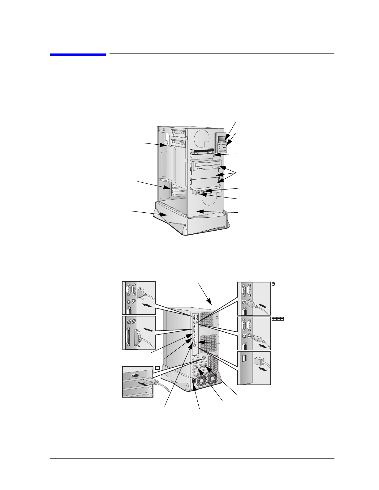
The following diagrams show the front and rear views of the HP VISUALIZE PersonalWorkstation.
Figure 1-1. Front View of the Personal Workstation
HP MaxiLife LCD buttons
Two internal mass storage
shelves 3.5 inches wide.
Upper shell: 1-inch high
Lower shelf: 1.6-inches high
Up to six accessory boards
can be installed:
One AGP slot,
Four 32-bit PCI slots,
One combination slot
ISA/PCI
Power Supply Unit
LCD Status Panel
Two 3.5-inch wide shelves
(including the floppy disk
drive)
Three 5.25-inch wide by
1.6-inch high front-access
shelves (including CD
drive)
Headphone Jack
Microphone Jack
Four spare screws (these
are to be used to secure
the system board in place
only).
Figure 1-2. Rear View of the Personal Workstation
Serial Ports A and B
Parallel Port
Line Out Jack
MIDI/Joystick Connector
Display Connector
Line In Jack
Key Lock
RJ 45 LAN Connector
Power Connector
Mic.
In
Jack
SCSI connector
Mouse Connector
Keyboard
Connector
Two USB
Connectors
Chapter 1 19
Page 20

System Overview
Internal Features
Internal Features
The core architecture of the HP Visualize Personal X-Class Workstation is constructed around
four buses: Host Bus, Peripheral Component Interconnect (PCI) Bus, Accelerator Graphics Port
(AGP) Bus and Memory Bus.
This PersonalWorkstation includes the Intel Pentium® III Xeon™ processor with 512 KB or1MB
of cache memory. This Personal Workstation can support up to two Pentium III Xeon processors.
This processor is described in the section “Intel Pentium III Xeon Processor” in the chapter
“System Board.”
The components of the system board are described in the chapter “System Board.” The
characteristics of the Personal Workstation’s video, disk and networking devices are described in
the chapter “Interface Boards and Mass-Storage Drives.” The HP BIOS routines are summarized
in the chapter “HP BIOS.” The Power-On Self-Test routines are described in the chapter “Tests
and Error Messages.”
20 Chapter1
Page 21
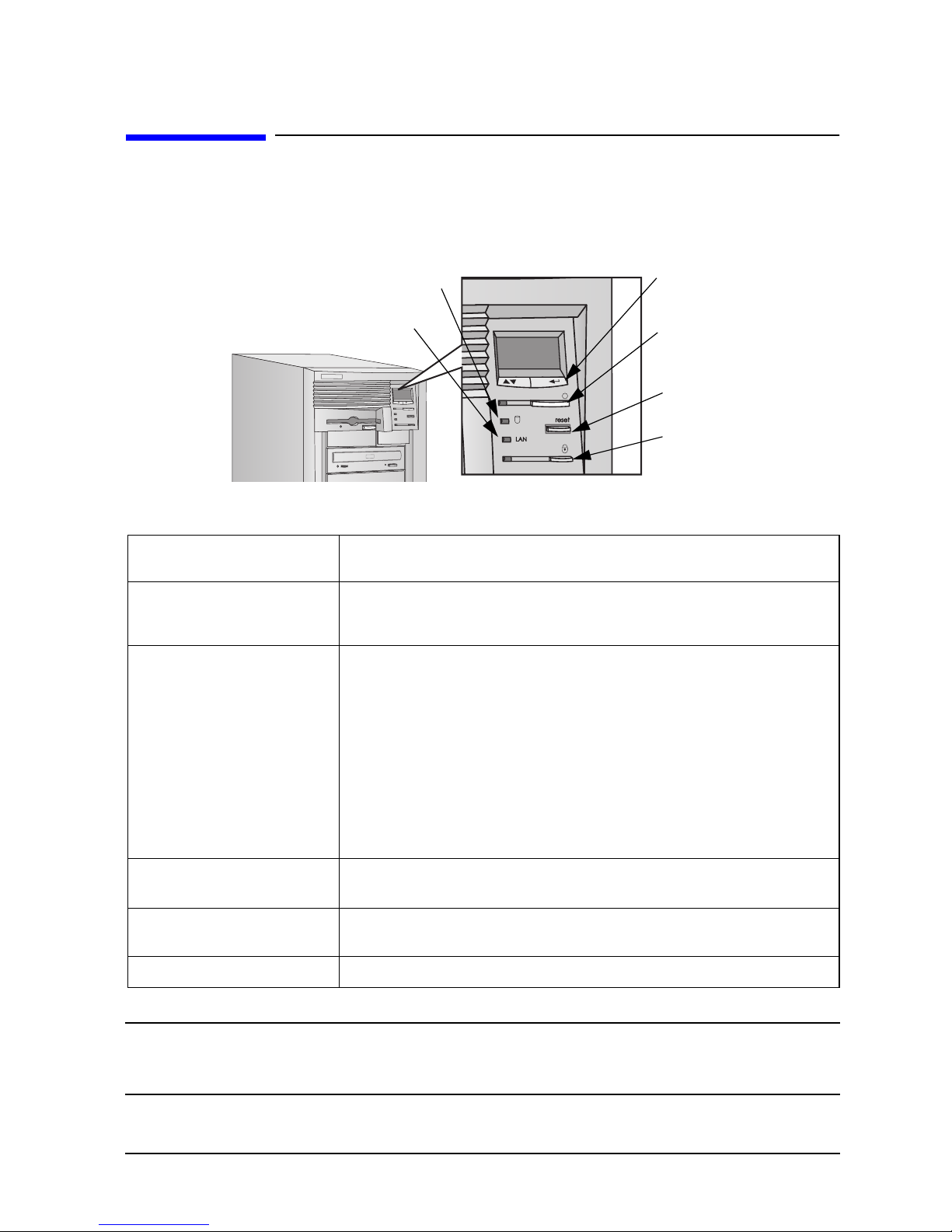
System Overview
Front Panel
This section explains the HP VISUALIZE Personal X-Class Workstation’s front panel features.
Figure 1-3. Front Panel Features of the Personal Workstation
Front Panel
Hard Disk Activity Light
Network Activity Light
MaxiLife LCD
Control Buttons
Power On/Off
Button and LED
Reset Button
PC Lock Button
and LED
Table 1-2. Front Panel Features and Their Descriptions
Liquid Crystal Display (LCD) The MaxiLife control panel menus are described in detail in the section “MaxiLife
Architecture” in the chapter “System Board.”
PC Lock Button
On/Off LED
This button has the same functionality as the multimedia keyboard “lock key.” When
HP Lock is installed under Windows NT 4.0, pressing this button is equivalent to “NT
Lock Workstation.” If HP Lock is not install, then this feature will not work.
This light has four states:
Blank Indicates that the computer is off.
Green Indicates that the computer is turned on and running
correctly.
Red Indicates that there is a Power-On Self-Test (POST)
error. Red flashing indicates that there is a MaxiLife
(Diag/Alarm) error.
Amber Indicates a system reset, system lock, standby mode
(Windows 98) or suspend mode (Windows 95).
Hard Disk Drive Activity
This light is active during POST and when the hard disk drive is being accessed.
LED
LAN Activity LED
Lock LED (Amber)
NOTE
The front panel volume control that was available on previous generations of
This light is active when the Personal Workstation is accessing the network. For this
feature to work, specific LAN HP drivers need to be installed.
This light is displayed when the system is locked.
the HP VISUALIZE Personal Workstations has been removed. Volume can now
be controlled using the keyboard or the software volume control.
Chapter 1 21
Page 22
System Overview
Specifications and Characteristics Data
Specifications and Characteristics Data
This section contains information regarding the physical characteristics, electrical specifications,
power consumption and environmental specifications of the HP VISUALIZE Personal X-Class
Workstation.
Table 1-3. Physical Characteristics
Characteristic Description
Weight (excl. keyboard and display) 22 kilograms (48.4 pounds)
Dimensions 41.6 cm (D) by 27 cm (W) by 51 cm (H)
16.38 inches (D) by 10.63 inches (W) by 20.08
inches (H)
Footprint
0.09 m2 (0.95 sq. ft.)
Table 1-4. Electrical Specifications
Parameter Total Rating Notes Maximum
Input Voltage 100-127
Vac
Input current
(max)
Output Power 350 W
Input Frequency 45 Hz to 66 Hz
Available Power
12 A 6 A
Max current
at +12 V
Max current at
−12 V
Max current at
+3.3 V
200-240
Vac
350 W
10 A — 0.5 A 0.2 A
0.8 A
45 A 7.6 A —
Selected
automatically
— 0.1 A 0.5 A —
per PCI
Slot
85 W combined
Maximum
for ISA
Slot
1
Maximum for
AGP Slot
65 W (max)
1 A
Imax(Vcc) = 6A
Imax(Vddq)= 8A
Max current at
+5 Vd (drivers)
Max current
9 A — — —
34 A 5 A 1 A 2 A
at
+5 Vm
(system
board)
Max current at
−5 A
0.5 A — — 0.2 A —
22 Chapter1
Page 23

Table 1-4. Electrical Specifications
System Overview
Specifications and Characteristics Data
Parameter Total Rating Notes Maximum
per PCI
Slot
Max current
0.72 A
—
—— —
Maximum
for ISA
Slot
Maximum for
AGP Slot
at
+5 Vstdby
1. PCI and AGP power electrical specifications must be respected. For example, the maximum power
consumption for the PCI slot is 25 W. The total power PCI consumption must never exceed 85 W. For the
AGP slot, 2 A maximum at +5 V.
An attempt to draw too much current (such as, a short circuit across edge-connector pins, or an
accessory board that is not suitable for these Personal Workstations), will cause the overload
protection in the power supply to be triggered, and the Personal Workstation could fail to boot.
NOTE
When the Personal Workstation is turned off with the power button on the
front panel, the power consumption falls below the low power level (refer to
Table 1-5), but is not zero. The special on/off method used by this Personal
Workstation extends the lifetime of the power supply. To reach zero power
consumption in “off” mode, either unplug the Personal Workstation form the
power outlet or use a power block with a switch.
Chapter 1 23
Page 24

System Overview
Specifications and Characteristics Data
Table 1-5. Power Consumption
Power Mode Power Consumption
Operating 85 W (average)
Idle 75 W (average)
Off 6.5 W (average)
Table 1-6. Environmental Specifications
Environmental Specifications (System Processing Unit, with Hard Disk)
Operating Temperature +5˚C to +40˚ (+40˚F to +104˚F)
Storage Temperature −40˚C to +70˚C (−40˚F to +158˚F)
Over Temperature Shutdown +50˚C (+122˚F)
Operating Humidity
Storage Humidity
Acoustic noise emission:
Sound power – with 10.0krpm SCSI hard disk drive
Operating Altitude 10000 ft (3100m) max
Storage Altitude 15000 ft (4600m) max
1. Non-condensing conditions
15% to 80% (relative)
8% to 80% (relative)
(as defined by ISO 7779)
LwA < 50 db
1
1
Operating temperature and humidity ranges may vary depending upon the mass storage devices
installed. High humidity levels can cause improper operation of disk drives. Low humidity levels
can aggravate static electricity problems and cause excessive wear of the disk surface.
24 Chapter1
Page 25

Power Saving
Table 1-7. Power Saving
System Overview
Power Saving
Full On
Processor Normal Speed Normal Speed Halted Halted
Display On Blanked, < 30 W, on
Hard Disk Drive Normal Speed Normal Speed
Power
Consumption
Resume events Keyboard, mouse Keyboard, network
Resume delay Instantaneous
1. Available only on Windows 95.
40 W to 70 W
depending on
configuration
and activity
Standby
models with
integrated graphics
< 40 W (230V, 50 Hz)
< 26 W (115V, 50 Hz)
1
Suspend
Blank, < 5 W (typ) Blank, < 5 W (typ)
Halted Halted
< 40 W (230V, 50 Hz)
< 21 W (115V, 60 Hz)
(RPO)
A few seconds Boot delay
1
Shutdown
(Plugged in but
turned off)
0441- 6.5 W (average)
0480 - 6.1 W (average)
Space bar
Power-On from the Space-Bar
The power-on from the space-bar function is enabled provided:
• The computer is connected to a Power-On keyboard (recognizable by the Power-On icon
on the space bar).
• The function has not been disabled by setting SW-8 to the ON position on the system
board.
• The function has not been disabled in the Power menu of the setup program.
Soft Power Down
When the user requests the operating system to shutdown, the environment is cleared,
and the computer is powered off. Soft Power Down is available with the Windows NT
(when the Soft Power Down utility is used), Windows 95 and Windows 98 operating
systems.
Chapter 1 25
Page 26
System Overview
Documentation
Documentation
The table below summarizes the availability of the documentation that is appropriate to
the HP V
in paper-based form. Most documents are available as printable files from the HP division
support servers or from the HP Tools and Support CD-ROM.
Table 1-8. Documentation Information
ISUALIZE Personal X-Class Workstations. Only selected documents are available
Title Division Support Server Online at HP WWW
ISUALIZE Personal
HP V
X-Class Workstation
User’s Guide
ISUALIZE fx
HP V
Configuration and
Troubleshooting Guide
ISUALIZE fx Texture
HP V
Module Installation
Guide
ISUALIZE Personal
HP V
X-Class Workstation
Service Handbook
Network Administrator’s
Guide
Using Sound on Your
Personal Workstation
MaxiLife Guide
Site (see address below)
PDF file
PDF file PDF file A5021-90011
PDF file PDF file A5021-90010
PDF file
PDF format
(in LAN Drivers Disk 2)
PDF format PDF file No
PDF format
PDF file A5014-90013
PDF file A5014-90039
PDF file No
PDF file No
Paper-based
Where to Find the Information
Table 1-9 summarizes the availability of information within the HP VISUALIZE Personal
Workstation documentation set.
Table 1-9. Where to Find the Information
Product Features
Product Model
numbers
26 Chapter1
User’s Guide Service Handbook Technical Reference
Manual
Introducing the Personal Workstation
Exploded view
Part list
Product range
CPL dates
Key features
Page 27

Table 1-9. Where to Find the Information
User’s Guide Service Handbook Technical Reference
Using the Personal Workstation
System Overview
Documentation
Manual
Connecting Cables
and Turning On
Finding Online
Information
Environmental
Formal Documents
Opening the Personal
Workstation
Supported Accessories
Installing Accessories
Configuring
Accessories
Fields and their
Options within Setup
Keyboard, mouse,
display, network,
printer, audio,
external, SCSI, power
Preloaded, HP web
sites
Setting up the
Personal Workstation
License Agreement
Warranty Information
Upgrading the Personal Workstation
Full details
Full part number
details
How to install mass
storage devices
Installing devices
Basic Complete list
Repairing the Personal Workstation
Troubleshooting
Technical Information Basic Advanced
System Board
BIOS Basic details
Power-On Self-Test
Routines (POST)
ISUALIZE Personal
HP V
Workstation Utility
Basic, MaxiLife,
hardware diagnoses
Basic details
Service Notes Advanced
Jumpers,switches and
connectors
Jumpers, switches and
connectors
Chip-set details
Technical details
Memory maps
Error codes and
suggestions for corrective
action
Order of tests
Technical details
Chapter 1 27
Page 28

System Overview
Documentation
Table 1-9. Where to Find the Information
User’s Guide Service Handbook Technical Reference
Peripheral Devices
Manual
Audio Accessories
LAN Accessories
Refer to the Audio
User’s Guide for
information on setting
up and configuring
audio accessories
Refer to the LAN
Administrator’s Guide
for information on
setting up and
configuring LAN cards
and systems.
Access HP World Wide Web Site
Additional online support documentation, BIOS upgrades and drivers are available from
HP’s World Wide Web site. To get to HP’s web side, us this URL:
http://www.hp.com/go/visualizesupport
28 Chapter1
Page 29

2 System Board
This chapter describes the components of the system board, taking in turn the components of the Host
Bus, the Peripheral Component Interconnect (PCI) bus, the System Management (SM) bus, the Industry
Standard Architecture (ISA) bus and the AGP Accelerated Graphics Port Controller.
29
Page 30
System Board
System Board Overview
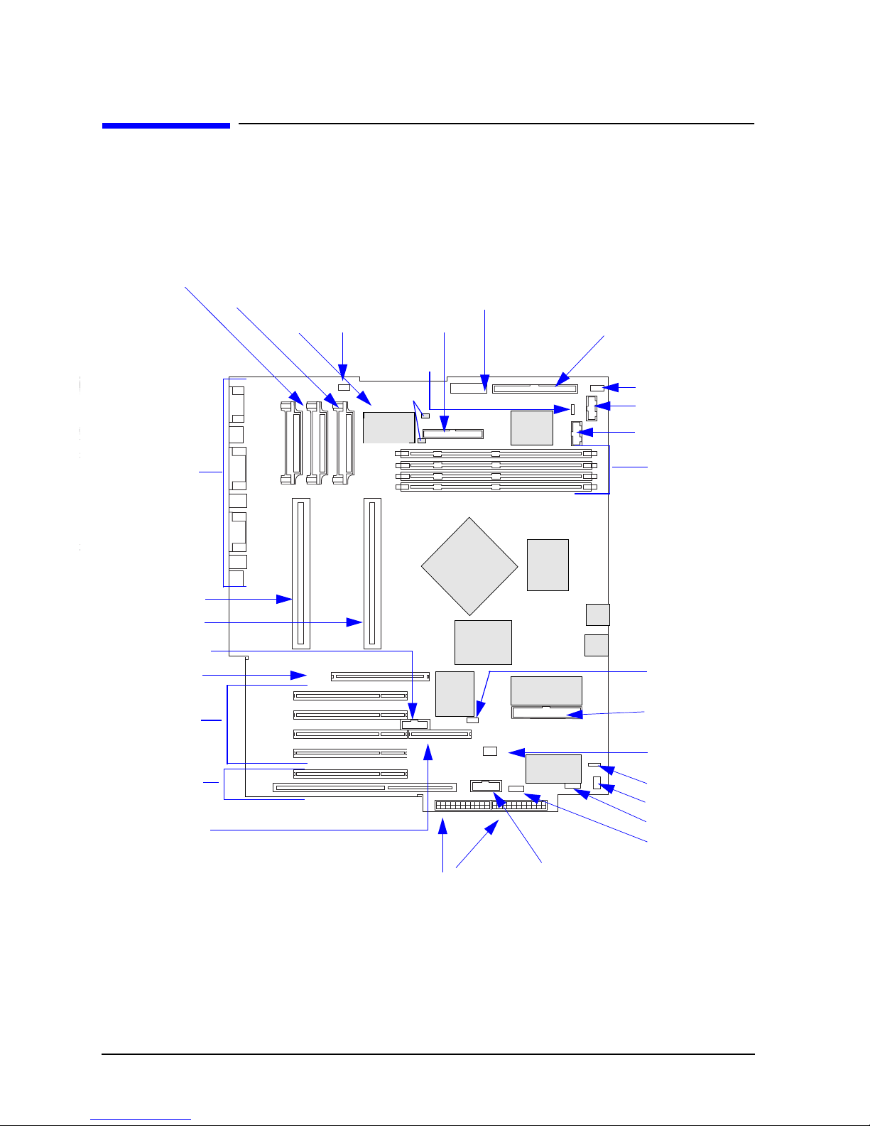
System Board Overview
The following diagram shows where the different chips and connectors are located on the
system board.
Figure 2-1. Location of the Chips and Connectors on the System Board
VRM 1 - J42
Rear Panel Connectors
Processor 1 Slot
Processor 2 Slot
HP External Start - J22
One AGP Slot - J34
Four PCI Slots
One PCI/ISA
Combination Slot
RAIDport - J23
VRM 2 - J36
Processor Fan
- J33
VRM3 - J30
BOOT PROC
Floppy Disk
DriveConnector
- J21
External
Battery - J8
2 Serial
EEPROMs
MaxiLife
ASIC
DUAL PROC
System
Board
Switches
440GX
Host Bridge
Adaptec
AIC7880
PIIX4E
1
Wide 16-bit SCSI
Connector - J14
(used for hardware monitoring)
NS317
Super
Main
PLL
2 X Flash
EEPRO
M
IO APIC
Audio
AD1816
Hard Disk Drive Fan - J3
Status Panel - J4
LCD Status Panel - J7
Mem 4 - X3
Mem 3 - X4
Mem 2 - X5
Mem 1 - X6
Wake On Lan - J19
Ultra DMA IDE
Connector - J13
I/O Cards Fan - J15
Internal Speaker - J1
Aux In Audio - J2
CD In Audio - J5
Mic In - J11
1. Refer to the Switch Block Label located on the chassis of thesystem box
for the different system board switch settings.
30 Chapter2
Power Supply
Connectors - J17 & J10
Multimedia Panel J16
Page 31

Architectural View
Figure 2-2. Architectural View
On each processorthere
is a SMBus EEPROM
and SMBus Thermal
SEC car-
Xeon Processor with L2
Intel Pentium III
cache memory
SMBus
Intel Pentium III
Xeon Processor
(optional second proces-
sor) with L2 cache mem-
System Board
Architectural View
SEC cartridge
Graphics
Local Mem-
Video
BIOS
(32 bit, 33
133 MB/sec.
PCI Bus
MHz)
Address (32)
Control
Data (64)
Internal
DMA
Connector
AGP
Graph-
ics
AGP Bus
(32-bit, 66 MHz
(2X), 528 MB/sec
data transfer rate)
Adaptec
AIC7880
16-bitSCSI
Controller
Internal16-bit
SCSI Connec-
IDE
USB 1
USB 2
440GX
Host Bridge
82443GX
PCI Bus
Interface
PCI/ISA
Bridge
(PIIX4E)
IDE
Control-
2 x USB
Control-
Memory Bus
(72-bit ECC
100 MHz, 800
MB/ sec data
transfer rate)
SMBus
Control-
DMA
Control-
Interrupt
ControlISA Bus
Interface
Main Memory
PCI Slots
MaxiLife
Monitoring Chip
4 DIMMS
(Serial Presence Detect)
Clock
Clock
SMBus
LCD
ISA Slot
Host (also called
FSB) Bus (64 bit,
100 MHz, 800
MB/sec data
transfer rate)
LAN + SCSI
Combination Slot
RAID-
CK4
D
Serial
EEPR
SMBus
ISA Bus
(16 bit, 8.33 MHz)
Two
29F002T
1
The graphics board depends on the model of Personal Workstation.
Chapter 2 31
Intel 82093 IO APIC
external interrupt con-
Super I/O
NS 97317
AD-1816
Audio
Combination Slot
Page 32

System Board
Accessory Board Slots
Accessory Board Slots
The following block diagram shows the position of the accessory board slots on the system
board.
Figure 2-3. Accessory Board Slots
One AGP slot. Can be used for a
graphics controller.
Four PCI slots. Can be used for a
32-bit PCI board. PCI Slot 3 has a
RAIDport for the HP FastRAID
board.
J34 (AGP Slot)
J37 (PCI Slot 1)
J38 (PCI Slot 2)
J39 (PCI Slot 3)
+RAIDport (J23)
J40 (PCI Slot 4)
One Combination slot. Can be used
for either a full-length 32-bit PCI or a
full-length 16-bit ISA board.
System board edge
J41 (PCI Slot 5)
J46 (ISA Slot
AGP Slot
The Accelerated Graphics Port (AGP) bus, provides a high performance graphics interface.
It uses a 66 MHz base clock, and provides a peak bandwidth of 528 MB/second.
AGP supports several modes, which are listed below. In its basic mode, AGP is very much like a 66 MHz
PCI bus; in a more advanced mode, pipelining is added along with special sideband signals, thereby
improving the bus performance. A double-clocking mechanism enables data transfers on both rising and
falling edges of the clock, which brings the maximum bandwidth to 528 MB/s: 66 MHz x 2
(double-clock) x 4 (bus width = 32 bit).
The different AGP modes include:
• Basic AGP: 66 MHz, PCI-like. Bandwidth: 265 MB/s.
• Pipelined AGP: 66 MHz + pipeline.
• Sideband AGP: 66 MHz + pipeline + sideband signals.
• Full AGP: 133 MHz equivalent (66 MHz with double clocking) + pipeline + sideband
signals. Bandwidth: 528 MB/s.
The AGP bus interface is explained in the section “Accelerated Graphics Port (AGP)
Controller.”
32 Chapter2
Page 33

System Board
Accessory Board Slots
PCI Slots
There is a total of five Peripheral Component Interconnect (PCI) connectors on the system
board. From top to bottom, the PCI slots are numbered 1 to 5 (refer to the diagram on the
previous page). The third PCI connector has a special extension called ARO or FastRaid
connector (refer to the section “FastRAID Port” for details about this connector), into which
the HP FastRAID accessory board can be installed. The fifth PCI connector shares the
corresponding slot with an ISA connector. This slot is called a Combo (Combination) slot,
since a PCI board or an ISA board can be installed in it.
The system board and BIOS support the PCI specification 2.1. It fully supports PCI-to-PCI
bridges and multi-function PCI devices, and each of the five PCI slots has Master
capabilities.
The maximum supported power consumption per slot is 25W, either from the 5V or the
3.3V supply and must respect the electrical specifications of the PCI 2.1 specification. Total
power consumption for the PCI slots must not exceed 85W.
The power consumption of each PCI board is automatically reported to the system through
the two Presence Detect pins of each PCI slot. These pins code the following cases:
• No accessory board in the PCI slot.
• 7W maximum PCI board in the PCI slot.
• 15W maximum PCI board in the PCI slot.
• 25W maximum PCI board in the PCI slot.
This information is reported in the BIOS setup screen. If the total power used in the PCI
slots exceeds 85W, the BIOS will display a warning during the boot sequence.
In addition to these PCI slots, there are three other devices connected on the PCI Bus:
• 440GX AGPset chipset, bridge between the Processor Front Side Bus (FSB) and the PCI
bus.
• PIIX4E chip, bridge between the PCI and the ISA, USB and IDE buses.
• AIC 7880 chip from Adaptec, PCI to SCSI (wide) controller.
Devices on the PCI bus are explained in the section “Devices on the PCI Bus” in this
chapter.
ISA Connector
There is only one ISA connector provided on the system board. The corresponding slot is
shared with the PCI connector (Combo slot).
In addition to this ISA slot, the following devices (refer to the section “Devices on the ISA
Bus” in this chapter for more details about devices on the ISA bus) are also connected to
the ISA bus:
• Ultra I/O (NS 97317), which integrates one parallel port, two serial ports, a keyboard
and mouse controller (8042), a floppy controller and a battery backed-up Real Time
Clock + CMOS (RTC).
Chapter 2 33
Page 34

System Board
Accessory Board Slots
• PIIX4E chip, bridge between the PCI and the ISA, USB and IDE buses.
• Two flash ROM sockets for 256 KB or 128 KB ROMs.
• Audio chip (AD1816 from Analog Device).
• IO APIC interrupt controller (Intel 82093).
The ISA bus interface is explained in the section “ISA Bus Interface” in this chapter.
FastRaid Port
A FastRaid port is provided on the system board through the ARO (RAIDport) connector.
This connector, aligned with the PCI slot 3, is to be used by a specific PCI accessory board,
called the ARO board. This board uses the ARO connector on the system board to directly
connect a SCSI hardware accelerator to the embedded Adaptec AIC 7880 controller. The
SCSI hardware accelerator chip, located on the ARO board, uses local memory to perform
hardware caching and also accelerates SCSI data striping when two hard disk drives are
used.
34 Chapter2
Page 35

System Board
System Board Switches
System Board Switches
The first system board switch is reserved (clock dithering spread spectrum), and the next
four switches set the ratio of processor-frequency to Processor-Local-Bus-Frequency. The
next five switches set the configuration for the Personal Workstation, as summarized in
the table below.
Table 2-1. System Board Configuration Switches
Switch Switch Function Default
1 Off Reserved - Do not use. (OFF = dithering is enabled, ON = dithering not enabled) Off
2 - 5 – Bus Frequencies (refer to the table “Bus Frequencies” in this
chapter).
6
Off
On
7
Off
On
8
Off
On
9
Off
Retain or clear the CMOS configuration stored in serial EEPROM:
Retain CMOS configuration.
Clear CMOS and reload default values in Setup.
Enable or disable User and System Administrator Passwords stored
in EEPROM:
Enable passwords.
Disable/Clear User and System Administrator passwords.
Keyboard power-on:
Disable keyboard power-on.
Enable keyboard power-on.
Frequency selection mode:
1
Enable automatic processor frequency, which is programmed by
MaxiLife.
–
Off
Off
On
On
On
10
Off
On
1. Automatic processor frequency is not yet available. Switch 9 should always be set to ON.
2. Refer to “BIOS Update Crisis Recovery Procedure” in this chapter.
Chapter 2 35
Enable manual processor frequency. System board switch settings
must be manually programmed.
Boot block:
Disable crisis recovery. Normal operation.
Enable crisis recovery. Recovery boot active2.
Off
Page 36

System Board
System Board Switches
System Board Switch Boxes
There are two types of system board switch boxes that may be used on the HP VISUALIZE
Personal Workstations.
Figure 2-4. Two Types of System Board Switch Boxes
OFF = ON =
OFF = ON =
36 Chapter2
Page 37

System Board
Chipset
Chipset
The Intel® 440GX AGPset chipset is comprised of the 82443GX Host Bridge/Controller
and, the 82371EB (PIIX4E) chip, which is a highly integrated version of the Intel PCI-ISA
bridge family for the I/O subsystem.
• The Host Bridge, also referred to as the North Bridge, is the bridge between four buses:
the Front Side Bus (FSB), the main memory (SDRAM) bus, the PCI bus and the AGP
(graphic) bus.
• The PIIX4E chip, also referred to as the South Bridge, is the bridge between three
buses: the PCI bus, the SMBus and the ISA bus. In addition, it contains the IDE
controller, USB controller and Power Management logic, Interrupt controller, Real Time
Clock (RTC) and CMOS. The table “PIIX4E (82371EB)” in this chapter details the
PIIX4E chip features.
Host Bridge/Controller (82443GX)
The Host Bridge/Controller is contained in a 492-pin Ball Grid Array (BGA) package. The
following table shows the features that are available in the Host Bridge/Controller.
Table 2-2. Features Available in the Host Bridge/Controller
Feature Feature
Processor/Host Bus Support
• Optimized for Pentium® processor at: 100
MHz system bus frequency.
• Supports full Symmetric Multiprocessor
(SMP) Protocol for up to two processors; I/O
APIC related buffer management support
(WSC# signal).
• In-order transaction and dynamic deferred
transaction support.
• Desktop optimized GTL+ bus driver
technology (gated GTL+ receivers for
reduced power).
AGP Interface
• Supports single AGP-compliant device
(AGP-66/133 3.3V
device).
• AGP Specifications Rev. 1.0 compliant.
• AGP-data/transaction flow optimized
arbitration mechanism.
• AGP side-band interface for efficient request
pipelining without interfering with the data
streams.
• AGP-specific data buffering.
• Supports concurrent CPU, AGP and PCI
transactions to main memory.
• AGP high-priority transactions (“expedite”)
support.
Chapter 2 37
Page 38

System Board
Chipset
Table 2-2. Features Available in the Host Bridge/Controller
Feature Feature
Integrated DRAM Controller
• Up to 2 GB with registered DIMMs (4 x 512
MB)1.
• Supports up to four double-sided DIMMs (8
rows memory).
• 64-bit data interface with ECC support
(SDRAM only).
• Unbuffered and Registered SDRAM
(synchronous) DRAM support (x-1-1-1
access at 100 MHz).
• Enhanced SDRAM Open Page Architecture
Support for 16-, 64-, 128- and 256-Mbit
DRAM devices with 2k, 4k and 8k page
sizes.
PCI Bus Interface
• PCI Rev. 2.1, 3.3V and 5V, 33 MHz interface
compliant.
• PCI Parity Generation Support.
• Data streaming support from PCI to
DRAM.
Power Management Functions
• Stop Clock Grant and Halt special cycle
translation (host to PCI bus).
• “Deep Green” Desktop supports for system
suspend/resume (i.e., DRAM and power-on
suspend).
• SDRAM self-refresh power down support in
suspend mode.
• Independent, internal dynamic clock gating
reduces average power dissipation.
• Static STOP CLOCK support.
• Power-on Suspend mode.
• Suspend to DRAM.
• ACPI-compliant power management.
Supporting I/O Bridge
• System Management Bus (SMB) with
support for DIMM
Serial Presence Detect (SPD).
• PCI-ISA Bridge (PIIX4E).
• Power Management Support.
• Delayed Transaction support for
PCI-DRAM Reads.
• Supports concurrent CPU, AGP and PCI
• 3.3V core and mixed 5V, 3.3V I/O and
interface to the 2.5V CPU signals via
open-drain output buffers.
transactions to main memory.
Packaging/Voltage
• 492-pin BGA.
• 3.3V core and mixed 3.3V and GTL I/O.
1. 82443GX Host Bridge Controller also supports 2 GB of unbuffered DIMMs (256Mbit
technology).
38 Chapter2
Page 39

System Board
Chipset
Host Bridge Interface
The Pentium III Xeon processor supports a second level cache via a Dual Independent Bus
(DIB). All control for the L2 cache is handled by the processor. The Host Bridge provides
bus control signals and address paths for transfers between the processors FSB (host bus),
PCI bus, AGP and main memory. The Host Bridge supports a 4-deep in-order queue (i.e.,
supports pipelining of up to four outstanding transaction requests on the host bus). Due to
the system concurrency requirements, along with support for pipelining of address
requests from the host bus, the Host Bridge supports request queueing for all three
interfaces (Host, AGP and PCI).
Host-initiated I/O cycles are decoded to PCI, AGP or PCI configuration space.
Host-initiated memory cycles are decoded to PCI, AGP (prefetchable or non-prefetchable
memory space) or DRAM (including AGP aperture memory). For memory cycles (Host, PCI
or AGP initiated) that target the AGP aperture space in DRAM, the Host Bridge translates
the address using the AGP address translation table. Other host cycles forwarded to AGP
are defined by the AGP address map.
PCI and AGP initiated cycles that target the AGP graphics aperture are also translated
using the AGP aperture translation table. AGP initiated cycles that target the AGP
graphics aperture mapped in main memory do not require a snoop cycle on the Host bus,
since the coherency of data for that particular memory range will be maintained by the
software.
The chip can support one or two Pentium III Xeon processors, at up to 100 MHz FSB clock
frequency. Refer to the section “Host Bus” in this chapter for a description of the devices on
the Host Bus.
PCI Bus Interface
The Host Bridge/Controller provides the interface to a PCI bus interface operating at 33
MHz. This interface implementation is compliant with PCI Rev 2.1 Specification,
supporting up to five external PCI masters in addition to the PIIX4E Bridge chip and the
Adaptec AIC 7880 16-bit SCSI controller. The PCI-to-DRAM interface can reach a transfer
rate of over 100 MBytes/sec for streaming reads and over 120 MBytes/sec for streaming
writes.
Sequential PL-to-PCI memory write cycles are translated into PCI zero wait state burst
cycles. The maximum PCI burst transfer can be between 256 bytes and 4 KB. The chip
supports advanced snooping for PCI master bursting, and provides a pre-fetch mechanism
dedicated for IDE read.
Refer to the section “Devices on the PCI Bus” in this chapter for a description of the devices
on the PCI Bus.
AGP Bus Interface
A controller for the AGP (Accelerated Graphics Port) slot is integrated in the Host
Bridge/Controller. The AGP Bus interface is compatible with the Accelerated Graphics
Port Specification, Rev 1.0, and it can support up to 133 MHz data transfer rates. The Host
Bridge/Controller supports only a synchronous AGP interface, coupling to the host bus
frequency. AGP characteristics are described in detail in the section “Accelerated Graphics
Port (AGP) Controller” in this chapter.
Chapter 2 39
Page 40

System Board
Chipset
Main Memory Controller
The main memory controller supports four DIMM sockets; Mem 1, Mem 2, Mem 3 and
Mem 4. Each socket can host a 168-pin SDRAM memory module, running at 100 MHz, and
can support unbuffered and registered memory modules. Each DIMM socket is connected
to the SMBus.
The Intel 440GX AGP set provides DIMM plug-and-play support via the Serial Presence
Detect (SPD) mechanism using the SMBus interface. The Host Bridge provides optional
data integrity features including ECC in the memory array. During reads from DRAM, the
Host Bridge provides error checking and correction of the data. The Host Bridge supports
multiple-bit error detection and single-bit error correction when the ECC mode is enabled
and single/multi-bit error detection when correction is disabled. During writes to the
DRAM, the Host Bridge generates ECC for the data on a QWord basis. Partial QWord
writes require a read-modify-write cycle when ECC is enabled.
The memory bus is 72-bits wide, comprised of 64 bits of data and 8 bits of ECC. Refer to the
section “Main Memory Bus” in this chapter for more detail on the main memory.
Read/Write Buffer
The Host Bridge defines a data buffering scheme to support the required level of
concurrent operations and provide adequate sustained bandwidth between the DRAM
subsystem and all other system interfaces (CPU, AGP and PCI).
System Clocking
The Host Bridge operates the host interface at 100 MHz, PCI at 33 MHz and AGP at
66/133 MHz. Coupling between all interfaces and internal logic is done in a synchronous
manner. The clocking scheme uses an external clock synthesizer (which produces reference
clocks for the host, AGP and PCI interfaces).
I/O APIC
I/O APIC is used to support dual processors as well as enhanced interrupt processing in
the single processor environment. The Host Bridge supports an external status output
that can be used to control synchronization of interrupts in configurations that use PIIX4E
with stand-alone I/O APIC components.
40 Chapter2
Page 41

System Board
Chipset
The PIIX4E, PCI/ISA Bridge Chip (82371EB)
The PCI-to-ISA/IDE Xcelerator chip, known as PIIX4E, is encapsulated in a 324-pin Ball
Grid Array (BGA) package.
The PIIX4E chip is a multi-function PCI device implementing a PCI-to-ISA bridge
function, a PCI IDE function, a Universal Bus host/hub function, and an Enhanced Power
Management function.
The following figure shows an example of the system block diagram using the PIIX4E chip.
Figure 2-5. System Block Diagram Using the PIIX4E Chip
PCI Bus (3.3V or 5V, 32-bit 33 MHz, 132 MB/sec data
Adaptec
AIC7880
16-bitSCSI
Controller
PCI/ISA Bridge
Hard
Internal16-bit
SCSI Connec-
SCSI
Terminator
USB
USB
Interrupt
Control-
PCI Bus
Interface
2 x USB
Control-
(PIIX4E)
DMA
Control-
SMBus
Control-
ISA Bus
Interface
IDE
Control-
General Purpose [I,O] (30+)
SMBus
CD-RO
PCI Slots
Combina-
LAN + SCSI
RAID-
ISA Slot
ISA/EIO Bus (5V, 16-bit, 8.25 MHz, 16 MB/sec data
Two
29F002T
BIOS
Intel 82093 I/O APIC
external interrupt con-
Keyboard, Mouse, Serial
Ports, Parallel Port,Floppy
Super I/O
NS 97317
Combination
AD-1816
Audio
Chapter 2 41
Page 42

System Board
Chipset
PIIX4E (82371EB)
Table 2-3. PIIX4E (82371EB) Chip Features
Feature Feature
Multifunction PCI to ISA Bridge, supports
• PCI at 30 MHz and 33 MHz.
• PCI Rev 2.1 Specification.
• Full ISA or Extended I/O (EIO) Bus.
• Full Positive Decode or Subtractive Decode
of PCI.
• ISA and EIO at of PCI Frequency.
Supports both Mobile and Desktop Deep
Green Environments
• 3.3V Operation with 5V Tolerant Buffers.
• Ultra-low Power for Mobile Environments
Support.
• Power-On Suspend, Suspend to RAM,
Suspend to Disk, and Soft-Off System
States.
• All Registers Readable and Restorable for
Proper Resume from 0.V Suspend.
Power Management Logic
Enhanced DMA Controller
• Two 82C37 DMA controllers.
• Supports PCI DMA with 3 PC/PCI
Channels and Distributed DMA Protocols
(simultaneously).
• Fast Type-F DMA for reduced PCI Bus
usage.
Interrupt Controller Based on TWo 82C59
• 15 Interrupt support.
• Independently programmable for
Edge/Level sensitivity.
• Supports Optional I/O APIC.
• Serial Interrupt Input.
Integrated IDE Controller
• Global and Local Device Management.
• Suspend and Resume Logic.
• Supports Thermal Alarm.
• Support for external microcontroller.
• Full support for Advanced Configuration
and Power Interface (ACPI) Revision 1.0
specification, and OS Directed Power
Management.
USB
• Two USB 1.0 Ports for Serial transfers at
12 or 1.5 Mbit/sec.
• Supports UHCI Design Guide.
• Independent Timing of up to four drives.
• PIO Mode 4 and Bus Master IDE transfers
up to 14 Mbytes/sec.
• Supports “Ultra DMA/33” Synchronous
DMA Mode transfers up to 33 Mbytes/sec.
• Integrated 16 x 32-bit buffer for IDE PCI
Burst transfers.
• Supports Glue-less “Swap-Bay”.
• Option with Full Electrical Isolation.
Real Time Clock
• 256-byte battery-backed up CMOS SRAM.
• Includes Date Alarm.
• Two 8-byte Lockout Ranges.
42 Chapter2
Page 43

Table 2-3. PIIX4E (82371EB) Chip Features
Feature Feature
System Board
Chipset
Timers Based on 82C54
• System Timer, Refresh Request, Speaker
Tone Output.
324 mBGA Package
SMBus
• Host Interface allows CPU to communicate
via SMBus.
• Slave interface allows external SMBus
Master to control
Resume Events.
PCI to ISA/EIO Bridge
PIIX4E compatible with the PCI Rev. 2.1 specification, as well as the IEEE 996
specification for the ISA (AT) bus. On PCI, PIIX4E operates as a master for various
internal modules, such as the USB controller, DMA controller, IDE bus master controller,
distributed DMA masters, and on behalf of ISA masters. PIIX4E operates as a slave for its
internal registers or for cycles that are passed to the ISA or EIO buses.
ISA Bus Interface
As well as accepting cycles from the PCI bus interface, and translating them for the ISA
bus, the ISA bus interface also requests the PCI master bridge to generate PCI cycles on
behalf of a DMA or ISA master. The ISA bus interface contains a standard ISA bus
controller and data buffering logic. Refer to the section “Devices on the ISA Bus” in this
chapter for a description of the devices on the ISABus.
SMBus Controller
The System Management (SM) bus is a two-wire serial bus provided by the PIIX4E
controller. It runs at a maximum of 16 kHz. The SMBus Host interface allows the CPU to
communicate with SMBus slaves and an SMBus Slave interface that allows external
masters to activate power management events. The bus also monitors some of the
hardware functions of the main board, both during boot-up and run-time. All accesses to
the bus are handled by the main processor, via the PIIX4E SMBus registers. Refer to the
section “Devices on the SMBus” for a description of the devices on the SMBus, or to the
section “HP MaxiLife Utility” in this chapter for information on the MaxiLife ASIC.
IDE Controller
The PCI master/slave IDE controller (Bus Master capability and synchronous DMA mode),
supporting two devices is described in the section “Integrated Drive Electronics (IDE)” in
this chapter.
Chapter 2 43
Page 44

System Board
Chipset
Enhanced USB Controller
The USB (Universal Serial Bus) controller provides support for the Universal Host
Controller Interface (UHCI). This includes support that allows legacy software to use a
USB-based keyboard and mouse. The USB supports two stacked connectors on the back
panel. These ports are built into the PIIX4E controller, as standard USB ports. The USB is
described in detail in the section “Universal Serial Bus (USB) Controller” in this chapter.
DMA Controller
The seven-channel DMA controller incorporates the functionality of two 82C37 DMA
controllers. Channels 0 to 3 are for 8-bit DMA devices, while channels 5 to 7 are for 16-bit
devices (see the section “DMA Channel Controllers” in the chapter “HP BIOS”). The
channels can be programmed for any of the four transfer modes: the three active modes
(single, demand, block) can perform three different types of transfer: read, write and verify.
The address generation circuitry supports a 24-bit address for DMA devices.
Interrupt Controller
Based on two 82C59 interrupt controllers. The two interrupt controllers are cascaded so
that 14 external and two internal interrupts are possible. In addition, PIIX4E supports a
serial interrupt scheme. It also supports the onboard I/O APIC controller 82093AA. A table
in the section “Interrupt Controllers” in the chapter “HP BIOS” shows how the master and
slave controllers are connected.
Counter / Timer
The chip contains a three-channel 82C54 counter/timer. Three counters are combined to
provide the system timer function, refresh request, and speaker tone. The counters use a
division of the 14.318 MHz OSC input as the clock source.
Serial EEPROM
This is the non-volatile memory which holds the values for the Setup program (they are no
longer stored in the CMOS memory). The Serial EEPROM is described in the section
“Serial EEPROM” in this chapter.
44 Chapter2
Page 45

System Board
Hot Bus
Hot Bus
The Host bus of the Pentium III Xeon processors, also referred to as the FSB (Front Side
Bus), is implemented in the AGTL (Assisted Gunning Transceiver Logic)+ technology. This
technology features open-drain signal drivers that are pulled-up to 1.5 V through resistors
at bus extremities; these resistors also act as bus terminators, and are integrated in the
processor. If only one processor is installed, a terminating board must be installed in the
second processor slot.
The supported operating frequencies of the AGTL+ bus is 100 MHz. The width of the data
bus is 64 bits, while the width of the address is 32 bits.
The control signals of the Host bus allow the implementation of a “split -transaction” bus
protocol. This allows the Pentium III Xeon processor to send its request (for example, for
the contents of a given memory address) and then to release the bus, rather than waiting
for the result, thereby allowing it to accept another request. The Intel 440GX, as target
device, then requests the bus again when it is ready to respond, and sends the requested
data packet. Up to four transactions are allowed to be outstanding at any given time.
For the Host bus to run at 100 MHz while respecting the specified signal and timings, a
distributed mechanism is used on each AGTL+ signal. The following termination resistors
are used: 150 ohm on the system board (close to the 440GX), 85 ohm on the system board
between the two processor slots. The bus is routed with a star topology.
Intel Pentium III Xeon Processor
The Pentium III Xeon processor has several features that enhance performance:
• Single Edge Contact Cartridge (S.E.C.C) package technology first introduced on the
Pentium II processor. This packaging technology allows Pentium III Xeon processors to
implement the Dual Independent Bus Architecture and have up to 2 MB of level 2
cache. Note that like the Pentium Pro and Pentium II Xeon processors, level 2 cache
communication occurs at the full speed of the processor core.
• MMX™ technology instructions, which gives enhanced media and communication
performance.
• Streaming SIMD Extensions for enhanced floating point and 3D application
performance.
The Pentium III Xeon processor (core and cache memory) is packaged in a self-contained
Single Edge Contact (SEC) cartridge installed in a Slot 2 processor slot. The SEC cartridge
requires a 330-contact Slot 2 connector on the system board. It includes a processor chip,
tag and data SRAMS, and AGTL+ termination resistors, SMBus ROM, and SMBus
thermal sensing device.
The Pentium III Xeon processor requires two different voltages to supply the CPU core and
L2 cache. Each processor codes through Voltage Identification (VID) pins with the required
voltage level being 1.8 to 3.5V. Two VID sets are provided, one for the CPU core, and one
for the L2 cache. Each VID set is decoded by a Voltage Regulation Module (VRM), installed
in a VRM socket on the system board, which supplies the required power voltage to the
processor.
Chapter 2 45
Page 46

System Board
Hot Bus
On HP VISUALIZE Personal Workstations there are two Slot 2 processor slots, along with
three VRM sockets. A single Pentium III Xeon processor for Slot 2 must be accompanied by
two VRMs inserted in VRM sockets 1 and 2 (from left to right). Single processor models
can be upgraded to a dual processor system by installing a second processor accessory in
the vacant slot. The second processor must be a Pentium III Xeon processor for Slot 2 of
the same speed and Level 2 cache memory capacity as the first, and same Level 2 cache
voltage. The VRM that was supplied with the second processor must be installed in the
vacant third VRM slot.
NOTE
When upgrading from a single processor to a dual processor with the
Hewlett-Packard processor accessory kit, you only need to check the processor
frequency speed and Level 2 cache memory capacity. This information can be
obtained by checking the label on the upper side of the processor. Processors
supplied with the Hewlett-Packard accessory kit are checked to ensure that
the Level 2 cache voltage is the same for all processors, and they have the
same frequency speed and Level 2 cache memory size.
It should be noted that Pentium III processors for Slot 1 are not compatible with Pentium
III Xeon processors for Slot 2. This means that you cannot upgrade a processor from a Slot
1 system to Slot 2.
The following table shows a comparison between the Pentium III Xeon processor for Slot 2
and Pentium III processor for Slot 1.
Table 2-4. Comparison between the Pentium III Xeon and Pentium III Processors
Feature Pentium III Xeon Processor for Slot 2 Pentium III Processor for Slot 1
Supported AGPset Intel 440GX Intel 440FX/LX/BX
Processor Core Speed 500 MHz, 550 MHz 266 MHz, 333 MHz, 350MHz,
400 MHz, 450 MHz or 500
MHz
System Bus Speed 100 MHz only 66 MHz or 100 MHz
Level 2 Cache Bus Speed Full Processor Core Speed Half Processor Core Speed
Level 2 Cache Size 512 KB, 1 MB, or 2 MB (for servers) 512 KB
Processor Slot 330-pin size connector 242-pin size connector
46 Chapter2
Page 47

System Board
Hot Bus
Bus Frequencies
There is a 14.318 MHz crystal oscillator on the system board. This frequency is multiplied
to 100 MHz by a phase-locked loop. This is further scaled by an internal clock multiplier
within the processor.
For example, the Pentium III Xeon 400 MHz processor multiplies the 100 MHz system
clock by 4. Switches 2, 3, 4 and 5 set the clock multiplier ratio.
Table 2-5. Switches for Setting the Clock Multiplier Ratio
Processor
Frequency
2345 9
400 MHz OFF ON OFF OFF ON 4
450 MHz OFF ON OFF ON ON 4.5
500 MHz OFF ON ON OFF ON 5
550 MHz OFF ON ON ON ON 5.5
1. Switches are provided to match the system board to processorfrequency when a system
board repair is performed.
It should be noted that on the HP V
Switch
ISUALIZE Personal Workstations, there are two types of
1
Frequency Ratio
Processor:
Local Bus
system board switch boxes. These are shown the section “System Board Switch Boxes” in
this chapter. A table summarizing switches six through to ten is shown in the section
“System Board Switches” in this chapter.
The computer may execute erratically, if at all, or may overheat, or won’t boot if it is
configured to operate at a higher processor speed than the processor is capable of
supporting. This can cause damage to the computer.
If the switches are set to operate at a slower speed than the processor is capable of
supporting, this may also cause erratic behavior in some cases and would reduce the
instruction throughput in others.
Cache Memory
There can be either two integrated circuits (core + 1 cache = 512 KB L2 cache) or three
integrated circuits (core + 2 cache = 1 MB L2 cache) sealed within a single Pentium III
package. One of these contains the Level-2 (L2) cache memory chip; the other contains the
processor, which itself includes Level-1 (L1) cache memory.
The L1 cache memory has a total capacity of 32KB (16 KB data, 16 KB instructions). The
L2 cache memory has a capacity of 512 KB or 1 MB, and is composed of four-way
set-associative static RAM. Data is stored in lines of 32 bytes (256 bits). Thus two
consecutive 128-bit transfers with the main memory are involved in each transaction.
The amount of cache memory is set by Intel at the time of manufacture, and cannot be
changed.
Chapter 2 47
Page 48

System Board
Hot Bus
Optional Second Microprocessor
HP VISUALIZE Personal Workstations have dual processing capability. Installing a second
processor is only advantageous when the software can make use of parallel activity. In
particular, you need to be running a multi-threaded operating system that supports
multiprocessing (one that is MPS-ready), such as Windows NT. The Windows NT operating
system makes the best use of the Pentium III’s 32-bit architecture (though other operating
systems will also show some benefit if 32-bit application programs are run).
The following table summarizes the supported operating systems:
Table 2-6. Summary of Supported Operating Systems
Windows NT 4.0 (or greater) Windows 95 and Windows 98
Multi-threaded Yes Yes
MPS-ready Yes No
32-bit operating system Yes
32-bit applications available Yes Yes
1. 32-bit operation at the outermost levels, but only 16-bit working internally.
Partial
1
The two processors must be operating at the same processor speed, and both, or neither,
must support the processor internal ECC functionality.
Configuring Setup for Multi-Processing
HP V
ISUALIZE Personal Workstations support Symmetric Multi-Processing (SMP). When
adding a second processor, you must ensure that: (a) the “multi-processing” choice has
been made in the system Setup; (b) the operating system supports multi-processors.
In the case of Windows NT, it might be necessary to perform an upgrade from the MPS
uniprocessor to the MPS multi-processor version.
NOTE
The system Setup allows a choice between “mono or multi-processing”
operations. The “mono-processing” mode has been implemented in order to
support operating systems that rely on the “legacy” interrupt controller
82C59 and are not aware of I/O APIC controller 820093AA operation. Refer to
the section “Interrupt Controllers” in the chapter “HP BIOS” for further
details.
48 Chapter2
Page 49

System Board
Main Memory Bus
Main Memory Bus
The memory bus is 72-bits wide, comprised of 64 bits of data and address information, and
8 bits of Error Correcting Code (ECC). The bus is connected to the Main Memory and to
the Host Bridge (Intel 440GX) chip.
HP V
ISUALIZE Personal Workstation models are supplied with a 128 MB unbuffered ECC
SDRAM memory module in one of the four DIMM slots, leaving the other slots free for
memory upgrades. If additional memory is required, up to 1 GB (4 x 256 MB) of unbuffered
memory may be installed. Memory upgrades are available in single 64 MB, 128 MB or 256
MB unbuffered ECC SDRAM modules.
Or, alternatively, the existing unbuffered memory modules may be replaced by Registered
ECC SDRAM memory modules. Memory can be upgraded to a maximum of 2 GB using
multiples of 512 MB Registered or unbuffered ECC SDRAM memory modules (4 x 512
MB). Both the 512 MB Registered and unbuffered memory modules were not available at
the time of introduction of the HP V
ISUALIZE Personal Workstations
NOTE
Unbuffered and Registered ECC memory modules are not compatible with
each other, and cannot be mixed.
Refer to the section “DIMM Sockets” in this chapter for information about the DIMM
sockets.
Chapter 2 49
Page 50

System Board
Main Memory Bus
Mixing Memory Modules
Unbuffered and Registered ECC modules are not compatible with each other, and cannot
be mixed. If they have been mixed, this will be detected in the basic pre-boot tests when
you boot the system for the first time. The BIOS checks that the inserted DIMMs are
compatible with one another and, if it detects an error, reports it to MaxiLife. The error
message (shown below) will then be displayed on the LCD status panel.
Error!
RAM type
Table 2-7. Memory Module Compatibility
Memory Module Compatibility Adding Unbuffered ECC Adding Registered ECC
(512 MB)
Unbuffered ECC Compatible Not Compatible
Registered ECC (512 MB) Not Compatible Compatible
Error Correcting Code Operation
Error correcting code (ECC) memory allows any single-bit error that occurs in any 72-bit
line of memory (64 data bits plus 8 parity bits) to be corrected (automatically and
transparently) by the host bridge chip.
The ECC detects single- and dual-bit errors. It can correct single bit errors during SDRAM
reads. The corrected data is transmitted to the requester (PCI or CPU) but not written
back to the SDRAM. A double-bit error would cause an NMI to be generated, and the PC
Workstation to be halted.
If more bits are faulty within any given 72-bit line, the effect is the same as it would have
been without error correction. The effect of executing a faulty instruction is always
unpredictable, and might cause the program to ‘hang’. The effect of reading a faulty data
word is often similarly unpredictable, but can sometimes be tolerated (for instance, it
might merely appear as a corrupted pixel on a video display).
50 Chapter2
Page 51

Devices on the PCI Bus
Table 2-8. Devices on the PCI Bus
System Board
Devices on the PCI Bus
PCI Device
PL/PCI Bridge
Virtual PCI-to-PCI Bridge
(AGP)
PCI/ISA Bridge
IDE Controller 1 – – – –
USB Host Controller 2 – – – –
Power Management and
SMBus
Ultra-wide (16-bit) SCSI
Controller
AGP Slot J34
PCI Slot #1 J37 16d 0-7 27 D A B C
PCI Slot #2 J38 17d 0-7 28 C D A B
PCI Slot #3 (ARO) J39 18d 0-7 29 A B C D
Device
Name
Intel440GX
Host Bridge
Intel440GX
Host Bridge
PIIX4E
AIC-7880 8 0 19 A
Device
Number
0
1 N/A ––––
7 0 18––––
Function IDSEL
AD(xx)
N/A ––––
3––––
0
Chipset Interrupt Connection
INTA INTB INTC INTD
AB
PCI Slot#4 SCSI/LAN Combo
Board
PCI Slot #5 J42 20d 0-7 31d D A B C
J40 19d 0-7 30 B C D A
The distribution of the interrupt lines is described more fully in the section “PCI Interrupt
Request Lines” in the chapter “HP BIOS.”
Ultra-Wide (16-bit) Small Computer System Interface (SCSI)
Controller
The Adaptec AIC-7880 Ultra-wide SCSI PCI controller is integrated on the HP VISUALIZE
Personal Workstation system board. Data is transferred at 40 MB/s on 16-bit wide,
single-ended bus. The controller is fitted with a 16-bit SCSI flat cable with five connectors,
plus a SCSI termination device; so a maximum of five internal wide-SCSI hard drives are
supported.
By default, the internal SCSI bus is configured to run in Ultra-SCSI mode (providing a
maximum band-width of 40 MB/s). The user may configure the SCSI system using the
SCSISelect utility, included in the system BIOS. This utility is described in more detail in
the SCSI User’s Guide.
Chapter 2 51
Page 52

System Board
Devices on the PCI Bus
SCSI-configured-automatically (SCAM) support is provided at level 2, for Plug and Play.
However, hot swap is not supported. The controller is BBS compliant.
The Ultra-wide SCSI controller and cable supports RAIDport PCI devices such as the HP
FastRAID solution (refer to the section “HP FastRAID2” in this chapter).
Integrated Drive Electronics (IDE)
The IDE controller is implemented as part of the PIIX4E chip. It is driven from the PCI
bus, and has PCI-Master capability. It supports Enhanced IDE (EIDE) and Standard IDE
channels. It also supports data rate up to 33 MBytes/second (Ultra DMA 33 mode). To use
the Enhanced IDE features the drives must be compliant with Enhanced IDE.
The IDE controller supports two devices (one master and one slave) connected to a single
channel. The channel is fitted with an IDE cable with two connectors.
It is possible to mix a fast and a slow device, such as a hard disk drive and a a CD-ROM, on
the same channel without affecting the performance of the fast device. The BIOS
automatically determines the fastest configuration that each device supports. However, in
general, the IDE cable is recommended for CD-ROM drives, and the SCSI cables for hard
disk drives.
Universal Serial Bus (USB) Controller
The USB controller is implemented as part of the PIIX4E chip. It is accessed through the
PCI bus, and provides support for the two stacked USB connectors on the back panel
individually. Over-current detection and protection is also provided.
Because the AGP connector defines a USB connection, it is possible to redirect one of the
two USB ports to the AGP connector. In this case, the second external USB port is
disabled. The over-current detection is shared between the second external USB port and
the AGP connector.
USB works only if the USB interface has been enabled within the HP Setup program.
Currently, only the Microsoft Windows 95 and Windows 98 operating systems provide
support for the USB.
The Microsoft Supplement 2.1 software (called USBSupp.exe), which provides support for
the Universal Serial Bus for Windows 95 Software Release (SR) 2.0, can be obtained from
the Hewlett-Packard WorldWideWeb site (refer to the section “AccessHP World Wide Web
Site” in the chapter “System Overview.”
52 Chapter2
Page 53

System Board
Devices on the PCI Bus
Other PCI Accessory Devices
PCI accessory boards are for high-speed peripheral accessories. A LAN/SCSI combo board
already occupies one of the PCI slots and the HP FastRAID board could occupy PCI Slot 3
(with the RAIDport). A diagram showing the PCI slots that are available for HP V
Personal Workstation models is in the section “System Board Overview” in this chapter.
Plug and Play
HP VISUALIZE Personal Workstations have a “PnP level 1.0A” BIOS and meet the
“Windows 95 Required” level for Plug and Play. Accessory boards which are Plug and Play
are automatically configured by the BIOS.
ISUALIZE
Chapter 2 53
Page 54

System Board
Accelerated Graphics Port (AGP) Controller
Accelerated Graphics Port (AGP) Controller
The AGP technology was developed to provide a dedicated bus for the graphics subsystem,
in order to meet the needs of high quality 3D graphics applications. The HP V
Personal Workstation is equipped with an AGP graphics controller.
The AGP bus is based upon a 66 MHz, 32 Bit PCI bus architecture, to which several signal
groups have been added. These additional signals provide AGP-specific control and
transfer mechanisms:
• Pipelining and sideband addressing. These control mechanisms increase the bus
efficiency in relation to the PCI protocol.
• Double clocking (2x mode). This is a transfer mechanism that doubles the peak transfer
rate to 528 MB/s, as two 32-Bit words are transferred in each clock period (2 x 32 bits x
66 MHz).
AGP specific transactions always use pipelining. The other two mechanisms can combine
independently to pipelining, which leads to the following operating modes:
ISUALIZE
• FRAME based AGP. Only the PCI protocol is used: 66 MHz, 32 Bits, 3.3V, 264 MB/s
peak transfer rate.
• 1 X AGP with pipelining, sideband addressing can be added: 66 MHz, 32 Bits, 3.3V,
increased bus efficiency, 264 MB/s peak transfer rate.
• 2 X AGP with pipelining, sideband addressing can be added: 66 MHz double clocked, 32
Bits, 3.3V, increased bus efficiency, 528 MB/s peak transfer rate.
AGP PCI Bus Implementation
In the diagram below, the AGP bus is viewed as a PCI bus with extra data lines.
Figure 2-6. AGP PCI Bus Implementation
Pentium II Xeon Proces-
Intel 440GX - Device 0
Host to PCI Bridge
PCI Bus # 0
PCI/ISA Bridge
AGP
Device
PCI Bus # 1
66 MHz
GX-Device 1
AGP Port
Virtual PCI-PCI Bridge
33 MHz
54 Chapter2
Page 55

System Board
Devices on the SMBus
Devices on the SMBus
The SMBus is a subset of the I2C bus. It is a two-wired serial bus which runs at a
maximum speed of 400 kHz. It is used to monitor some of the hardware functions of the
system board (such as voltage levels, temperature, fan speed, DIMM presence and type),
both at system boot and during normal run-time. It is controlled by the SMBus controller
located in the PIIX4E chip.
Table 2-9. Devices on the SMBus
Device SMBus Address
PIIX4E SMBus Master 10h
Processor Data EAh, E2h
Serial EEPROM A8h, AAh
LM75 (HDD temperature) 90h
Processor Temperature DCh, D8h
MaxiLife ASIC 28h
SDRAM Slot 1 A0h
SDRAM Slot 2 A2h
SDRAM Slot 3 A4h
SDRAM Slot 4 A6h
PLL D2h
LCD Panel 74h
The following devices are connected to the SMBus:
• PIIX4E SMBus Master Controller 16 kHz maximum.
• DIMM sockets.
• SDRAM clock buffer.
• Serial EEPROM.
• One LM75 temperature sensor.
• MaxiLife for hardware management, bus master controller 400 kHz
maximum.
• LCD status panel.
• CPUs serial EEPROM - Processor Information ROM (“PIROM”).
• CPUs thermal sensors.
Chapter 2 55
Page 56

System Board
Devices on the SMBus
An isolation mechanism is implemented, so that the LM75 temperature sensor, MaxiLife
monitoring chip, and the Serial EEPROM can be accessed even when the computer is
turned off. These devices are powered through Vcc standby. The PIIX4E and MaxiLife are
the two master devices.
PIIX4E SMBus Master Controller
The PIIX4E chip provides an intelligent processor-to-SMBus controller. All access is
handled by the processor through the PIIX4E SMBus interface. Typically, the processor
has access to all the devices connected to the SMBus.
DIMM Sockets
Each DIMM socket is connected to the SMBus. The 168-pin DIMM modules used on HP
V
ISUALIZE Personal Workstations include a 256 byte I2C Serial EEPROM. The first 128
bytes contain general information, including the DRAM chips’ manufacturer, DIMM speed
rating, DIMM type, etc. The second 128 bytes of the Serial EEPROM can be used to store
data online. This will be used to store such information as ECC errors and possibly some
manufacturing related data (date module built or first installed, etc).
SDRAM Clock Buffer
The I2C port of the SDRAM clock buffer is connected to the SMBus. It can be used to stop
the unused clocks.
Serial EEPROM
This is the non-volatile memory which holds the default values for the CMOS memory (in
the event of battery failure).
When installing a new system board, the Serial EEPROM will have a blank serial number
field. This will be detected automatically by the BIOS, which will then prompt the user for
the serial number which is printed on the identification label on the back of the PC
Workstation.
The computer uses 16KBytes of Serial EEPROM implemented within two chips. Serial
EEPROM is ROM in which one byte at a time can be returned to its unprogrammed state
by the application of appropriate electrical signals. In effect, it can be made to behave like
very slow, non-volatile RAM. It is used for storing the tatoo string, the serial number, and
the parameter settings for the Setup program and also MaxiLife firmware.
Xeon Thermal Sensors
These sensors are located within the Single Edge Contact (SEC) cartridge. They are used
to measure temperature within the CPU, and this information is used to regulate the CPU
fan speed.
56 Chapter2
Page 57

System Board
Devices on the SMBus
LM75 Temperature Sensor
The LM75 temperature sensor and alarm are located on the system board. The sensor is
used to measure the temperature in various areas of the system board. This information is
used, with other information, to regulate the hard disk drive fan and to send an alarm to
the processor when the temperature is above maximum and programmed minimum
thresholds.
Main PLL
The registers of the main PLL are accessed through the SMBus. These registers control
the PLL clock signal outputs and are write-only.
WARNING
Writing over the SMBus may be destructive to the PC Workstation as
it allows access to information necessary to the System BIOS,
without which the system will not run.
HP MaxiLife Utility
MaxiLife is a hardware monitoring chip which is resident on the system board. Its
responsibility includes On/Off and reset control, status panel management (Lock button,
LEDs), hardware monitoring (temperature and voltage), early diagnostics (CPU, DIMMs,
PLLs, boot start), run-time diagnostics (CPU errors, package intrusions), and other
miscellaneous functions (such as special OK/FAIL symbols based on a smiling face).
The integrated microprocessor includes a Synopsys cell based on Dallas “8052” equivalent,
a 2 KB boot ROM, 256 bytes of data RAM, an I2C cell, an Analog-to-Digital (ADC) with 5
entries, and an additional glue logic for interrupt control, fan regulation, and a status
panel control.
MaxiLife downloads its code in 96 milliseconds from an I2C serial EEPROM. The total
firmware (MaxiLife 8051-code, running in RAM) size is 8 KB. As it exceeds the 2 KB
program RAM space, a paging mechanism will swap code as it is required, based on a 512
byte buffer. The first 2 KB pages of firmware code is critical because it controls the initial
power on/reset to boot the system. This initial page is checked with a null-checksum test
and the presence of MaxiLife markers (located just below the 2 KB limit).
If the boot block has been corrupted, which prevents the system from powering on, the
Firmware can start from its ‘crisis’ block. To do this, set the System board switch 10 to the
On position. In order to reset the MaxiLife ASIC, unplug the power cord for more than 30
seconds before plugging it back in. Then power on the Personal Workstation and use the
BIOS bootblock recovery feature that is described in the section “BIOS Update Crisis
Recovery Procedure” in this chapter.
MaxiLife is partially replacing HP ASIC (Little Ben), and provides the necessary hardware
monitoring control. However, MaxiLife is not accessible in I/O space or memory space of
the system platform, but only through the SMBUS (which is a sub-set of the I2C bus), via
the PCI/ISA chipset (PIIX4E South Bridge). Its I2C cell may operate either in Slave or
Master mode, switched by firmware, or automatically in the event of ‘Arbitration’ loss.
Chapter 2 57
Page 58

System Board
Devices on the SMBus
As a monitoring chip, MaxiLife reports critical errors at start-up, and is therefore powered
by Vstandby (3.3V) power. For MaxiLife to work correctly, the Personal Workstation must
always be connected to a grounded outlet. This enables the Personal Workstation’s
hardware monitoring chip to be active, even if the system has been powered off.
Test Sequence and Error Messages
Refer to the section “MaxiLife Test Sequence and Error Messages” in the chapter “Tests
and Error Messages” for detailed information about the different test sequences and error
messages.
MaxiLife Architecture
The MaxiLife chip continuously monitors temperature and voltage sensors located in
critical regions on the system board. This chip receives data about the various system
components via a dedicated I2C bus, which is a reliable communications bus to control the
integrated circuit boards.
Figure 2-7. MaxiLife Chip Architecture
LCD Status Panel
I2C bus
Pentium II
Processor
PLLs
Intel 440GX
AGPset
Serial
DIMM
DIMM
DIMM
DIMM
HP MaxiLife
Speed up/slow down
Package
Intrusion
Sensor
Temperature
Sensors
System Fans
Voltage
Sensors
58 Chapter2
Page 59

System Board
Devices on the SMBus
The LCD Menu
To access the LCD main menu, press one of the LCD keys. This menu is composed of
several menu items which are displayed two at a time on the LCD screen. The following
menus are available:
• System Info. Obtains information from the BIOS and the system’s Serial EEPROM
from a previously successful boot. This information includes: product name, BIOS
version, serial number, the number of processors and speed, size of memory for each
DIMM socket.
The BIOS logs information in the serial EEPROM with SYSINFO.COM at the end of
the boot.
• Boot Steps. Shows the Power-On Self-Test (POST) codes during the system start-up.
The POST code is provided by the BIOS and is displayed on the LCD panel as soon as it
is available. If the system stops during the
start-up, the last successful boot step POST code is displayed on the LCD.
• Diagnostics. Runs a set of diagnostics assessing the system’s components (CPU
presence, CPU power errors, power supply, clocks, and DIMM presence). To view the
test results for each system component, press button. If no errors are detected, a
screen will display a smiling face. If an error is detected, an error screen appears
indicating the problem.
Using MaxiLife When the Computer Is Powered Off
NOTE
MaxiLife is powered by VSTBY. This means that it is functional as soon as
the power cord is plugged in. For MaxiLife to work correctly, the Personal
Workstation must always be connected to a grounded outlet.
Even if the computer is powered off (the LCD status panel will be blank), MaxiLife is still
running and monitoring the state of the LCD buttons. From this state, the diagnostics
program can be run by pressing one of these buttons. When the Power on option is
selected, the main power supply is started, enabling the hardware monitoring chip to
access the status of the computer’s components. Although the main power supply has been
started, the computer does not continue to complete a normal boot.
The system components are tested in sequence (press the Next button to move on to the
following test). When the diagnostics tests are complete, one of the following screens will
be displayed:
Diagnostics:
Done FAIL
Exit
Diagnostics:
Done OK
Exit
Chapter 2 59
Page 60

System Board
Devices on the SMBus
If no errors are detected, you can exit the test session, and the main power supply will be
turned off and the LCD status panel will become blank.
If an error is detected, a short message is displayed on the LCD status panel describing the
type of error (memory, processor) that occurred. For example, the message DIMM FOUND: 0
would be displayed if no memory modules could be located. You can then choose whether to
continue viewing the results of the remaining tests.
NOTE
If the Diags program is run when the system is off, it returns to the Off state
when exiting the test session. On/Off transitions are accompanied with a
‘Please wait’ screen to allow MaxiLife to power on and off correctly.
60 Chapter2
Page 61

System Board
Devices on the ISA Bus
Devices on the ISA Bus
Table 2-10. Devices on the ISA Bus
ISA Device Index Data
Ultra I/O 2Eh 2Fh
The Super I/O Controller (NS 97317)
The Ultra I/O chip (NS 97317) provides the control for two FDD devices, two serial ports
and one bidirectional multi-mode parallel port.
Serial / parallel communications ports
The 9-pin serial ports (whose pin layouts are depicted in the section “Socket Pin Layouts”
in the chapter “Interface Boards and Mass-Storage Drives”) supports RS-232-C and are
buffered by 16550A UARTs, with 16-Byte FIFOs. They can be programmed as COM1,
COM2, COM3, COM4, or disabled.
The 25-pin parallel port (also depicted in the section “Socket Pin Layouts” in the chapter
“Interface Boards and Mass-Storage Drives”) is Centronics compatible, supporting IEEE
1284. It can be programmed as LPT1, LPT2, or disabled. It can operate in the four
following modes:
• Standard mode (PC/XT, PC/AT, and PS/2 compatible).
• Bidirectional mode (PC/XT, PC/AT, and PS/2 compatible).
• Enhanced mode (enhanced parallel port, EPP, compatible).
• High speed mode (MS/HP extended capabilities port, ECP, compatible).
FDC
The integrated flexible disk controller (FDC) supports any combination of two of the
following: tape drives, 3.5-inch flexible disk drives, 5.25-inch flexible disk drives. It is
software and register-compatible with the 82077AA, and 100% IBM-compatible. It has an
A and B drive-swapping capability and a non-burst DMA option.
RTC
The real-time clock (RTC) is 146818A-compatible, with an accuracy of 20ppm (parts per
million). The configuration RAM is implemented as 256 bytes of CMOS. The RTC operates
on a 32.768 kHz crystal and a separate 3V goldcap that provides up to 3 weeks of
protection when the power cord is unplugged.
The century is stored in a register of the RTC and will automatically change from 1999 to
2000 (without BIOS intervention).
Chapter 2 61
Page 62

System Board
Devices on the ISA Bus
Keyboard and Mouse Controller
The computer has an 8042-based keyboard and mouse controller. The connector pin
layouts are shown in the section “Socket Pin Layouts” in the chapter “Interface Boards and
Mass-Storage Drives.”
Audio Controller
HP VISUALIZE Personal Workstations have an audio chip (AD1816) integrated on the
system board. This single chip is a Plug and Play multimedia audio subsystem for
concurrently processing multiple digital streams of 16-bit stereo audio.
Host Interface
The AD1816 audio chip contains all necessary ISA bus logic on chip. This logic includes
address decoding for all onboard resources, control and signal interpretation, DMA
selection and control logic, IRQ selection and control logic, and all interface configuration
logic.
Audio Chip Specifications
The audio chip is driven from the ISA bus, and has the following specifications:
Table 2-11. Audio Chip Specifications
Feature Description
Digitized Sounds • 16-bit and 8-bit stereo sampling from 4 kHz to 55.2 kHz
• Programmable sample rates with 1 Hz resolution
• Hardware Full Duplex Conversion
• 16-bit software-based real-time audio
compression/decompression system
Music Synthesizer • Integrated OPL3 compatible music synthesizer
Mixer • MPC-3 audio mixer
• Input mixing sources: microphone, LINE In,
CD Audio, AUX Audio, and digitized sounds
• Output mixing of all audio sources to the LINE Out or
integrated PC Workstation speaker
• Multiple source recording and Left/Right channels balance
Line Input • Input impedance: 17k W (ohms)
• Input range: 0 to 2.83 Vpp
Line Output • Stereo output of 100 mW per channel with headphone
62 Chapter2
speakers (impedance 32 Ω)
• Output impedance: 570 Ω
• Output range: 0 to 2.83 Vpp
Page 63

Devices on the ISA Bus
Table 2-11. Audio Chip Specifications
Feature Description
Audio Front Panel • Microphone input jack
• Stereo output jack
Microphone Input • 20 dB gain preamplifier. The boost can be muted with
software
• 32-level programmable volume control
• Input impedance: 600 W
• Sensitivity: 30 mVpp to 283 mVpp
Stereo Out Jack • Impedance: 32 W
The headphones jack and the stereo-out (audio) jack can be used interchangeably.
Flash EEPROM
System Board
The PC Workstation uses 512 KB of Flash EEPROM implemented using two 8-bit ROM
chips. Flash EEPROM is ROM in which the whole memory can be returned to its
unprogrammed state by the application of appropriate electrical signals to its pins. It can
then be reprogrammed with the latest upgrade firmware.
The System ROM contains the LAN boot firmware and the system BIOS (including the
boot code, the ISA and PCI initialization, the Setup program and the Power-On Self-Test
routines, video BIOS, plus their error messages). These are summarized the chapter “HP
BIOS” and the chapter “Tests and Error Messages.”
The Flash EEPROMs on HP V
ISUALIZE Personal Workstations implement a bootblock
feature which allows recovery from a failed attempt at updating the System BIOS. The
bootblock contains the minimum system BIOS information necessary to reprogram the
Flash EEPROM.
Updating the system ROM
The System ROM can be updated with the latest BIOS firmware. This can be downloaded
from HP’s World Wide Web site:
http://www.hp.com/go/visualizesupport
To download a BIOS upgrade, connect to the HP Web site and follow the on-screen
instructions to download the flash utility programs.
Before updating the System ROM, it is necessary to disable the “PSWRD” switch on the
system switches (SW-7), and to type in the System Administrator’s Password when
starting up the computer. The PCI and PnP information is erased in the process.
Do not switch off the computer until the system BIOS update procedure has completed,
successfully or not, otherwise irrecoverable damage to the ROM may be caused. While
updating the flash ROM, the power supply switch and the reset button are disabled to
prevent accidental interruption of the flash programming process.
Chapter 2 63
Page 64

System Board
Devices on the ISA Bus
BIOS Update Crisis Recovery Procedure
If, for example, during a BIOS update process, the process is interrupted by a power
failure, and the system does not start, you can still recover the situation of a destroyed
system BIOS. However, it should be noted that during the recovery procedure, there is no
image on the screen, nor access to the keyboard or mouse (only “vital” devices that are
required to boot on the floppy are initialized). Follow these steps to recover the BIOS:
1. Ensure that you have created a DOS-bootable diskette. This floppy diskette contains all
the recovery and system BIOS programming software (phlash.exe, platform.bin and
HO1xyyzz.Ful). Include the flash command in the first line of autoexec.bat, for example:
phlash /c HO1xyyzz.Ful
H = HP Professional PC
O = HP V
ISUALIZE Personal Workstation (Pentium II Xeon models)
1 = HP Division that provides the platform. In this case, it is PDCO
x = major revision
yy = minor revision
zz = language
NOTE
Setting Switch 10 to the Closed position also enables the MaxiLife firmware
‘crisis’ block if the power cord is unplugged (after approximately 30 seconds).
In this case, the LCD status panel is not available and the screen is blank.
2. Turn off the computer. Set Switch 10 to the Closed position.
3. Insert the DOS-bootable diskette.
4. Turn on the computer.
5. During the recovery process, short beeps are emitted. The recover process is finished
when there is a much longer beep (after approximately 1 to 2 minutes).
6. Power off the computer. Press the power ON/OFF button (for about 5 seconds), until the
ON/OFF light switches off. Set switch 10 to the Up position.
Other ISA Accessory Devices
ISA accessory boards are for slow peripheral accessories. A diagram showing the ISA slots
that are available for the HP V
Board Slots” in this chapter.
Plug and Play
All PCI accessory boards are Plug and Play, although not all ISA boards are. Check the
accessory board’s documentation if you are unsure.
In general, in a Plug and Play configuration, resources for an ISA board have to be
reserved first (using the Setup utility). Then you can plug in your board.
64 Chapter2
ISUALIZE Personal Workstations is in the section “Accessory
Page 65

System Board
Devices on the ISA Bus
The procedure for installing an ISA accessory board that is not Plug and Play is described
in the User’s Guide that is supplied with the Personal Workstation.
NOTE
The Windows NT 4.0 operating system is not Plug and Play. Information
given above is only applicable for Plug and Play operating systems (for
example, Windows 95).
Chapter 2 65
Page 66

System Board
Devices on the ISA Bus
66 Chapter2
Page 67

3 Interface Boards and Mass-Storage
Drivers
This chapter describes the video, mass storage, audio and network devices which are supplied with the
Personal Workstation. It also summarizes the pin connections on internal and external connectors.
67
Page 68

Interface Boards and Mass-Storage Drivers
ELSA GLoria Synergy+ AGP Graphics Board
ELSA GLoria Synergy+ AGP Graphics Board
HP VISUALIZE Personal Workstation models are supplied with an ELSA GLoria
Synergy+™ AGP graphics board fitted in the AGP accessory slot. There is a total of 8 MB
of video Synchronous Graphics RAM (SGRAM) memory installed on the graphics board
which cannot be upgraded.
The Permedia 2A graphics processor communicates directly with the Pentium II processor
along the AGP bus.
Features
• Optimized all-round capabilities in 2 D and 3 D.
• High resolution with 1900 x 1200 pixels in HiColor.
• 2D performance and high-power 3D hardware acceleration.
• Multi-screen support for Windows NT (with PCI ELSA GLoria Synergy+ graphics
boards).
• Supports 16: 10 wide-format monitors.
Specifications
• Supports basic AGP mode (66 MHz).
• Serial EEPROM video BIOS interface (up to 64 KB).
• AGP ATX form factor compliant.
• PERMEDIA 2A graphics processor.
• Pixel clock maximum frequency of 250 MHz.
• 3D coprocessor. Integrated GLINT Delta graphics setup processor.
• 3D standards. Hardware accelerated OpenGL, HEIDI, Direct3D.
• 4 MB of video SGRAM memory installed on the graphics board. Added to this, there is a
pre-installed 4 MB SO_DIMM video memory module, giving a total of 8 MB (this is the
maximum amount of video memory possible).
• Standards: VESA Video BIOS, DPMS, DDC2B, Plug & Play.
• Video standards: DirectDraw, ActiveMovie 1.0, DirectShow
(ActiveMovide 2.0).
68 Chapter3
Page 69

Interface Boards and Mass-Storage Drivers
ELSA GLoria Synergy+ AGP Graphics Board
Figure 3-1. ELSA GLoria Synergy+ AGP Graphics Board
1 MB SGRAM memory
chips installed on the
graphics board
Display
connector
4 MB SO_DIMM
installed memory chips
Permedia 2A
Graphics
processor
73
172,1 mm
1 MB SGRAM memory
chips installed on the
graphics board
Video Memory
The video memory, also known as SGRAM, is a local block of RAM for holding major data
structures: Frame Buffer (double buffer), Z-Buffer and T-Buffer (Texture Buffer). The
Frame Buffer holds one frame steady on the screen while the next one is being processed,
while the Z-buffer stores depth information for each pixel.
Chapter 3 69
Page 70

Interface Boards and Mass-Storage Drivers
ELSA GLoria Synergy+ AGP Graphics Board
Available Video Resolutions
The number of colors supported is limited by the graphics device and the video memory.
The resolution/color/refresh-rate combination is limited by a combination of the display
driver, the graphics device, and the video memory. If the resolution/refresh-rate
combination is set higher than the display can support, you risk damaging the display.
The tables below summarize the 3D video resolutions which are supported.
Table 3-1. Support 3D Video Resolutions
Resolution Max. Refresh Rate (Hz) / Z-Buffer, Double Buffering
256 Colors Hi Color (32,768) TrueColor (16.7 million)
640×480 pixels 60, 70, 75, 80, 85, 100 60, 70, 75, 80, 85, 100 60, 70, 75, 80, 85, 100
800×600 pixels 60, 70, 75, 80, 85, 100 60, 70, 75, 80, 85, 100 60, 70, 75, 80, 85, 100
1024×768 pixels 60, 70, 75, 80, 85, 100 60, 70, 75, 80, 85, 100 60, 70, 75, 80, 85, 100
1152×864 pixels 60, 70, 75, 80, 85, 100 60, 70, 75, 80, 85, 100 —
1280×1024 pixels 60, 70, 75, 80, 85, 100 60, 70, 75, 80, 85, 100 —
1600×1024 pixels 60, 70, 75, 80, 85, 100 — —
1600×1000 pixels 60, 70, 75, 80, 85, 100 — —
1536×1152 pixels 60, 70, 75, 80, 85 — —
1600×1200 pixels 60, 70, 75, 80, 85 — —
1600×1280 pixels 60, 70, 75, 80, 85 — —
70 Chapter3
Page 71

Interface Boards and Mass-Storage Drivers
HP Visualize fx OpenGL 3D Graphics Hardware Accelerator
HP VISUALIZE fx OpenGL 3D Graphics Hardware
Accelerator
HP VISUALIZE Personal Workstation models are supplied with an HP VISUALIZE fx Open
GL 3D graphics hardware accelerator. This graphics board requires two slots (1 AGP and 1
PCI) for installation.
There is a total of 18 MB of installed SGRAM memory on the graphics controller board. An
additional 16 MB or 32 MB of SDRAM texture memory can be added by installing a
texture module. This texture module is only available as an accessory for the HP
V
ISUALIZE fx video board.
NOTE
A similar texture module, supplying 16 MB of memory, exists for the HP
ISUALIZE fx
V
2
+ and fx4+ video boards used in the previous HP VISUALIZE
Personal Workstation models. These two texture modules cannot be
interchanged.
The HP V
ISUALIZE fx is a full length PCI accessory board which includes two connectors,
one for the AGP slot and one for the PCI slot. It is secured in place by two accessory board
slot screws and one for the support bracket. To improve the shock and vibration behavior
of this board, there is a long strengthening bracket along the top of the HP V
The diagram below shows the HP V
ISUALIZE fx Open GL 3D graphics hardware
ISUALIZE fx.
accelerator.
Figure 3-2. HP V
ISUALIZE fx Video Board (without an installed texture module)
Support bracket
Strengthening bracket to
improve shock and
vibration behavior.
Two terminator
sockets are
concealed beneath
this short
strengthening bar.
The longer of the
PCI
two sockets contains
a terminator when no
Chapter 3 71
AGP
Page 72

Interface Boards and Mass-Storage Drivers
HP Visualize fx OpenGL 3D Graphics Hardware Accelerator
Features
The HP VISUALIZE fx Open GL 3D graphics hardware accelerator includes the following
main features:
• Dual slot solution: (1 AGP + 1 PCI).
• Geometry engine using dedicated PA-RISC floating-point cells.
• Up to 1600×1200 true color single buffered at 75 Hz, or 1280×1024 true color double
buffered at 85 Hz.
• 18 MB of video memory (100 MHz SGRAM).
• VGA supported via daughter board.
• Texture module (optional) with up to 32 MB of additional SDRAM memory.
• Fog.
• Alpha blending.
• Stereo capability in separate window (requires special stereo device).
• Anti-aliased points and vectors.
• HP Color Recovery Dithering and HP Occlusion Culling Extension.
Graphics Board Architecture
The HP VISUALIZE fx Open GL 3D graphics hardware accelerator is actually made up of
several graphics boards:
• The main board contains the bridge chip (which provides the interface to the AGP bus),
two geometry accelerators, frame buffer memory, two rasterizer chips and the
RAMDAC chip.
• A VGA board is connected to the main board such that the video output is analog
switched between the RAMDAC and the VGA chip.
• An optional texture board with a dual texture mapping chip and 32 MB of SDRAM
memory, running at 100 MHz, that may be installed as an accessory.
The block diagram below shows the architecture of the HP VISUALIZE fx Open GL 3D
graphics hardware accelerator:
72 Chapter3
Page 73

Figure 3-3. Graphics Board Architecture
AGP Bus
Interface Boards and Mass-Storage Drivers
HP Visualize fx OpenGL 3D Graphics Hardware Accelerator
2 x
Texture
Map
Control
Texture Memory
32 MB SDRAM
Main
Board
Bridge Chip
2 X Raster-
izer
RAMDAC
3 X Geome-
try
Frame Buffer
Memory
VGA
PCI Board
Frame Buffer Memory
There are 18 MB of frame buffer memory in 100 MHz SGRAM modules installed on the
main board of the HP VISUALIZE fx Open GL graphics hardware accelerator. This memory
contains image data and depth data, comprised of:
• 48-bit image planes (24-bit double-buffered)
• 8-bit overlay planes
• 24-bit Z-buffer
• 4-bit Window ID
• 4-bit stencil
Chapter 3 73
Page 74

Interface Boards and Mass-Storage Drivers
HP Visualize fx OpenGL 3D Graphics Hardware Accelerator
Geometry Acceleration
The HP V
ISUALIZE fx Open GL graphics hardware accelerator is equipped with the world’s
fastest geometry accelerator ASIC. It consists of a hard-coded graphics processor
containing 2 integer ALUs, 2 floating-point multipliers, 2 floating point divider/square root
units and dual control. The geometry accelerator’s main features include:
• Provides geometry acceleration for vectors, 3- or 4-sided polygons, triangle strips and
fans.
• Performs lighting calculations for up to 8 directional or positional lights, in addition to
ambient lighting.
• Handles alpha and texture coordinates.
• Provides full acceleration for OpenGL pipelines.
• Is capable of efficient parallelism.
Texture Module
The texture module, containing 16 MB or 32 MB of texture memory (depending on your
Personal Workstation model), can be installed on the HP V
ISUALIZE fx Open GL graphics
hardware accelerator as an accessory. Installation of the texture module adds the following
features:
• 2D point, bilinear and trilinear sample modes
• MIP-mapping
• 3D texture mapping
• Shadow textures
Available Video Resolutions
The table below summarizes the video resolutions which are supported.
Table 3-2. Available Video Resolutions
Resolution Matrix
Resolution 24/8 bits
640×480 60, 85, 120 Hz
800×600 60, 85, 120 Hz
1024×768 60, 85, 120 Hz
1280×1024 60, 75, 85 Hz
1600×1200 60, 75 Hz
74 Chapter3
Page 75

Interface Boards and Mass-Storage Drivers
SCSI/LAN Combination Board
SCSI/LAN Combination Board
HP VISUALIZE Personal Workstations are supplied with an integrated SCSI / 10BT/100TX
LAN combination (combo)board which is installed in PCI Slot 4. Even though the
SCSI/LAN combo board includes two controllers, only one PCI slot is necessary for
installation.
The LAN and SCSI controllers access the PCI bus through a PCI-to-PCI bridge. The SCSI
and PCI functions are contained within the Symbios Logic SYM53C875JE PCI-SCSI I/O
Processor chip.
Do not connect any devices to the Internal Narrow SCSI connector, and to the Internal
Wide SCSI connector at the same time. If you do, this results in a badly “terminated” SCSI
bus. In the HP V
provided. The following diagram shows the SCSI/LAN Combo board connectors.
Figure 3-4. SCSI/LAN Combo Board Connectors
ISUALIZE Personal Workstations, only an Internal Narrow SCSI cable is
Thirteen-pin connector
(J4) to connect the
ExtStart cable to the
Three-pin connector
(J8) to connect the
WOL cable to the
Internal Wide SCSI
connector (J3 - not
LAN Controller
Optional Boot Rom
Socket (option)
External Wide SCSI
connector (J7).
LED which indicates
LAN link
RJ-45 connector.
PCI connector.
Refer to the section “System Board Overview” in
Chapter 2 to find out where the HP ExtStart and
WOL connectors are located on the system board.
Internal Narrow SCSI
connector (J9 - used).
Flash memory (128 KB)
Symbios Logic
(53C875JE)
PCI-to-PCI Bridge
PCI Interface
The PCI interface operates as a 32-bit DMA bus master. The connection is made through
the edge connector. The signal definitions and pin numbers conform to the PCI Local Bus
Specification Revision 2.1 standard. The PCI interface conforms to the PCI universal
signaling environment for a 5 volt PCI bus.
Chapter 3 75
Page 76

Interface Boards and Mass-Storage Drivers
SCSI/LAN Combination Board
SCSI Interface
The Symbios Logic SYM5C875JE PCI-SCSI I/O Processor chip connects the SCSI bus
directly and generates timing and protocol in compliance with the SCSI standard. The
following hardware functional diagram shows the SCSI part of the SCSI/LAN Combo
board.
Figure 3-5. SCSI Part of the SCSI/LAN Combo Board
External connector (16
Ext.
5V
Fuse 3A
SCSI
Bus
Termi-
nation
Termination
50-pin
Internal connector (16
68-pin high density
To ExtStart Connector
SCSI
LED connector
(not loaded)
68-pin high density
Osc.
40 MHz
EEPRO
2KB
M
Clock
Data
SCSI Controller
SYM53C875JE
PCI Bus
Internalconnector
(8 bits)
12V
VPP Transla-
tor
Flash Memory
28F010
128 KB
The SCSI interface operates as a 16-bit, synchronous or asynchronous, single-ended bus,
and supports Ultra SCSI protocols and 16-bit arbitration. The interface is made through
two (and only two) of the following connectors:
Table 3-3. SCSI Interface Connectors
Connector Description Location Comments
J3 Internal Wide SCSI connector.
Non-shielded 68-pin high density
right-angle receptacle.
J7 External wide SCSI connector.
Shielded 68-pin high density
right-angle receptacle.
J9 Internal narrow SCSI connector.
Non-shielded 50-pin low-density
straight receptacle.
Internal connector at
the end of the board.
Protrudesthrough the
rear panel bracket.
Located between the
Symbios Logic chip
and Internal side
SCSI connector.
Connectors J3 and J9
cannot be connected
to any devices at the
sametime. Ifthey are,
this results in a badly
“terminated” SCSI
bus. Refer to the
previous page for
further details.
76 Chapter3
Page 77

Interface Boards and Mass-Storage Drivers
SCSI/LAN Combination Board
Ultra Wide (16-bit) SCSI Controller
The Ultra wide 16-bit SCSI controller can support up to 15 devices (internal and external).
ISUALIZE Personal Workstations are supplied with a 16-bit wide external connector
HP V
and an 8-bit narrow internal cable (which can support up to two devices). Data is
transferred at 40 MB per second on a 16-bit wide, single-ended bus.
By default, the internal SCSI bus is configured to run in Ultra-SCSI mode (providing a
maximum band-width of 40 MB/s). The user may configure the SCSI system using the
SCSI Configuration Utility, included in the system BIOS. This utility is described in more
detail in the section “Symbios Logic SCSI Configuration Utility” in the chapter “HP BIOS.”
SCSI-configured-automatically (SCAM) support is provided at level 2, for Plug and Play.
However, hot swap is not supported. The controller is BIOS Boot Specification (BBS)
compliant.
SCSI/PCI LAN Combo Board Features
Table 3-4. SCSI/PCI LAN Combo Board Features
Interface Features
PCI Interface
SCSI Interface
Full 32-bit DMA bus master.
Zero wait-state bus master data bursts.
16-bit single ended.
Automatically enabled active termination.
Fast and Ultra SCSI data transfer capability.
SCSI TERMPWR source with auto-resetting circuit breaker.
SCAM (SCSI Configured AutoMatically).
Serial NVRAM (Non-Volatile RAM) for configuration utility and SCAM.
Flash BIOS.
Fast and Ultra SCSI controlled by external SCSI cable detection.
Ultra speed requires 1.5m maximum SCSI bus.
Chapter 3 77
Page 78

Interface Boards and Mass-Storage Drivers
SCSI/LAN Combination Board
10BT/100TX LAN Controller
The embedded 10BT/100TX LAN controller supports the following standards: 100 Mbits
per second over 2-pair, category-5, unshielded twisted pair (UTP), or shielded twisted pair
(STP); 10 BaseT, 10 Mbits per second, ISO 8802-3 (IEEE 802.3 standard).
The LAN adapter contains two internal connectors.
Table 3-5. 10BT/100TX LAN Adapter Internal Connectors
Connector Description Location
J4 External Start connector,13-pin. Enables LAN
activity, SCSI Led activity on the front panel
for harddisk drive accesses, andexternal SCSI
cable detection.
J9 Wake On LAN connector, 3-pin. Enables a host
computer to remotely power on computers
(over the network).
Located near the J9 connector.
Located between the J9 and J3
connectors.
• Wake On LAN (WOL) which enables a host computer, using Magic Packet technology, to
remotely (over the network) power on computers (Remote Power On) or wake them up
(Remote Wake Up) from energy-saving Sleep mode.
For these functions to work, the WOL cable must be connected between the three-pin
connector (J8), on the SCSI/LAN Combination board, and the WOL connector on the
system board. Refer to the section “SCSI/LAN Combination Board” in this chapter to
locate the position of the J8 connector on the SCSI/LAN combination board and refer to
the section “System Board Overview” in the chapter “System Board” for the WOL
connector on the system board.
The LAN adapter that uses the Remote Power On feature must be installed further
from the processors than any other supplementary LAN adapter card. How to use the
Remote Power On feature is described in detail in the User’s Guide provided with the
PC Workstation.
• External Start connector which enables LAN activity, the SCSI LED activity on the
front panel for SCSI hard disk drive accesses, and external SCSI cable detection.
The external cable must be connected between the thirteen-pin connector (J4), on the
SCSI/LAN combination board, to the HP External Start connector on the system board.
Refer to the section “SCSI/LAN Combination Board” in this chapter for the position of
the J4 connector on the SCSI/LAN combination board and refer to the section “System
Board Overview” in the chapter “System Board” for the HP External Start connector
position on the system board.
78 Chapter3
Page 79

Interface Boards and Mass-Storage Drivers
SCSI/LAN Combination Board
On the rear panel there is one RJ-45 connector. There is a LED which indicates the LAN
connection status as follows:
• Off - when there is no response (for example, when the LAN cable is not connected to
the network HUB.
• Blinking - during Autonegotiation
• Green (ON) - the connection has passed the Autonegotiation and a link has been
established between the LAN adapter and the network HUB/Switch.
NOTE
Refer to the User’s Guide for details concerning system configuration changes
necessary after installing a LAN adapter.
10BT/100TX LAN Features
Table 3-6. 10BT/100TX LAN Features
Feature Description
LAN Controller AMD PCNET-Fast+ chip
RJ45 Connector 10BT/100TX autonegotiation
Remote Boot Protocols integrated in System BIOS
ExtStart Connector Connection to CPU board
Remote Power On (RPO) Full remote power on with Magic Packet
Remote Wake Up (RWU) Wake Up from Suspend state with Magic Packet
Wake On LAN (WOL) Enables a host computer, using Magic Packet technology, to remotely
(over the network) power on computers.
Remote Power On
Remote Power On (RPO) is available at 10 and 100 Mbits per second.
Vstandby requirements supporting RPO
The Vstandby requirement for the HP network card supporting RPO, is: a power supply
able to deliver at least 720 mA on Vstandby output. This is the case for all HP V
systems.
Chapter 3 79
ISUALIZE
Page 80

Interface Boards and Mass-Storage Drivers
SCSI/LAN Combination Board
Optional BootROM Socket
It is possible to add a flash device on the network card socket with a specific LAN
BootROM code. This new BootROM code will be seen and mapped automatically by the
system BIOS instead of the embedded version (system BIOS).
NOTE
If you are looking for a specific or a new version of the BootROM, refer to the
LANWORKS web site at: http://www.lanworks.com.
Flash / ROM Devices
The 10BT/100TX card provides a PLCC 32-pin socket, and any size of flash device can be
used up to 256 KB.
Installing Two LAN Remote Power On Cards
From a network standpoint, it is possible to install two LAN RPO cards, and both cards
will be functional (for example, from the operating system, it will be possible to have two
LAN cards up and running at the same time).
However, there are restrictions due to the remote manageability boot features
implementation. To support these features, an internal cable is required between the LAN
card and the system board. However, only one card can be attached to this cable, so that
remote manageability features are supported on one card only.
The problem is that with the current BIOS and hardware implementation, it is not
possible to identify which LAN card the cable is attached to, and this may result in having
none of the remote capabilities working properly.
Even though it is possible to install two LAN Remote PowerOn cards in the computer, only
one card is seen by the BIOS setup. In conclusion, when installing two LAN cards, always
remember that it is very difficult implement the RPO functionality on a LAN card.
NOTE
Administrative tools (for example, TopTool Openview) are not capable of
identifying which network board WOL is connected to.
80 Chapter3
Page 81

Interface Boards and Mass-Storage Drivers
HP FastRAID2
HP FastRAID2
To improve performance of the 16-bit Wide Ultra SCSI channel, the new generation of HP
FastRAID is available as an option. Both HP V
of supporting the HP FastRAID2 Accessory Kit. When installing HP FastRAID2, please
refer to the Installation and Configuration Guide supplied with the HP FastRAID2
Accessory Kit for instructions.
ISUALIZE Personal Workstationsare capable
WARNING
HP FastRAID2 and HP FASTRAID1 software (BIOS, drivers and HP
Raid device manager) are NOT compatible.
Figure 3-6. HP FastRAID2 Board
The HP FastRAID2 solution (or Accessory Kit if ordered after purchase) includes an
Adaptec ARO2 PCI RAIDport adapter and five disks containing configuration utilities,
drivers and the CI/O Array Management software. Note that the CI/O Array Manager is
also known as the HP RAID Manager, and contains the ArrayConfig utility imbedded in it.
The Accessory Kit, along with the RAIDport connector and firmware on the system board
of the PC Workstation, provide the components necessary to implement FastRAID2.
The ARO2 adapter increases the performance of the PC Workstation’s hard drives by
accelerating data storage and retrieval. Part of this hardware acceleration is due to the
read and write cache options available with the ARO2 adapter. Using the write cache,
when the memory is flushed to the SCSI devices (hard drives), reduces the idle time is to
one tenth of the idle time without the FastRAID2 option. For certain applications, read
caching (i.e. pre-emptive reading and caching of sequential sectors of data, to have ready to
use if needed) can accelerate operations.
Chapter 3 81
Page 82

Interface Boards and Mass-Storage Drivers
HP FastRAID2
Read/write caching is an advantageous option, but the primary function of the FastRAID2
solution is to provide enhanced hard drive performance through two supported modes:
• Raid0 (default configuration): This configuration provides data read/write acceleration
using one or two hard drives (of the same capacity and speed) through disk striping. In
general terms, data blocks are divided and stored between two hard drives using a
method called disk striping. It is important to point out that there is no redundancy of
data storage, and the RAID 0 mode does not, in any way, reduce the necessity of backing
up stored data.
NOTE
To obtain the benefits of read/write caching using the ARO2 adapter in a
system with only one hard drive, it is necessary to select the RAID0 mode.
• Raid1 configuration: This configuration provides software mirroring and caching. Data
is mirrored (duplicated) using a hard disk pair. If one disk fails, the data is still
available on the mirrored drive. The RAID 1 configuration also provides an
improvement in performance using the cache on the ARO2 adapter. It does not,
however, provide the same throughput as the RAID 0 configuration. In addition,
because data is mirrored, the storage capacity of your drives is only half of the physical
capacity of the drives.
One of the above modes may be selected using the ArrayConfig utility. This utility is
described in detail in the User’s Guide supplied with the Personal Workstation.
The ARO2 adapter and hard drive(s) come pre-configured for maximum performance
(RAID 0) but may also be configured to provide protection against data loss (RAID 1).
CAUTION
Configurations RAID5 and RAID10 are not supported.
The ARO2 adapter is supplied with 16 MB SIMM installed in the adapter memory slot. If
the adapter must be replaced, do not remove the SIMM because the replacement adapter
will be supplied with its own SIMM. In addition, no re-configuration of the FastRAID2 I/O
subsystem is necessary following the replacement of the ARO2 adapter, as all information
concerning the FastRAID2 configuration is stored on the hard disk drive(s).
82 Chapter3
Page 83

Interface Boards and Mass-Storage Drivers
HP FastRAID2
The disk striping features offered by the HP FastRAID2 solution are summarized in the
following table:
Table 3-7. Disk Striping Features Offered by HP FastRAID2
Feature Description
Computer bus 32-bit PCI local bus and HP FastRAID2 socket connector
Host bus data transfer
rate (if cache enabled)
Device protocol Ultra wide 16-bit SCSI
Advanced HP FastRAID2
features
Array support • Drives can be configured for FastRAID2 levels 0 and 1
Operating system Windows NT 4.0
SCAM Not supported; SCSI addresses must be set manually on Ultra wide
Up to 133 MB per second
• User-defined rebuild priority
• User-defined verify priority
• Array status monitoring and event notification
• Adjustable stripe width
• Drives can also be supported in non-array environments
16-bit SCSI channel
Chapter 3 83
Page 84

Interface Boards and Mass-Storage Drivers
Mass-Storage Drives
Mass-Storage Drives
The Ultra-wide (16-bit) SCSI controller is described in the section “Ultra-Wide (16-bit)
Small Computer System Interface (SCSI) Controller” in the chapter “System Board.” The
flexible disk controller is described in the section “FDC” in the chapter “System Board.”
Hard Disk Drives
The following table lists the 3.5-inch (1-inch high) hard disk drives (which are subject to
change) that may be supplied (type and quantity depends on model) on internal shelves,
connected to the 16-bit Ultra-wide SCSI controller.
Table 3-8. Hard Disk Drives
9.1 GB UW-SCSI
10k rpm
Manufacturer Seagate
Product name Cheetah 9LP
Average seek time 5.4 ms
Revolutions per minute (RPM) 10000
Track to track transfer rate 0.98 ms
Maximum internal transfer rate 14.4 - 21 MB/s
Flexible Disk Drives
A 3.5-inch, 1.44 MB flexible disk drive (D2035-63121) is supplied on the top front-access
shelf of models.
CD Drives
IDE 32X CD-ROM Drive
Some models
shelf ATAPI, supporting ATAPI commands and with audio playback capability. It can play
any standard CD-Audio disks, in addition to CD-ROM disks, conforming to optical and
mechanical standards as specified in the Red and Yellow Book.
Some of the IDE 32X CD-ROM features include:
1
have a 32X Max IDE CD-ROM drive supplied in a 5.25-inch front-access
• Application Disk type (confirmed by Red, Yellow, Green, Orange Book).
• CD-ROM data disk (Mode 1 and Mode 2).
1. Refer to the HP VISUALIZE Personal X-Class Workstation Service Handbook to find out which
Personal Workstations are installed with an IDE 32X CD-ROM.
84 Chapter3
Page 85

• Photo-CD Multisession.
• CD Audio disk.
• Mixed mode CD-ROM disk (data and audio).
• CD-ROM XA, CD-I, CD-Extra, CD-R, CD-RW.
Table 3-9. IDE 32X CD-ROM Drive
HP product number D4384A
Disk Diameter 120mm
Data Block Size 2,048 bytes (Mode-1)
2,336 bytes (Mode-2)
Storage Capacity 650 Mbytes (Mode-1)
742 Mbytes (Mode-2)
Interface Boards and Mass-Storage Drivers
Mass-Storage Drives
Description
Read Mode
Full CAV1 14X to 32X
Burst Transfer Rate PIO mode 4 - 16.6 Mbytes/s maximum
Single Word DMA Mode 2 - 8.3 Mbytes/s maximum
Multi Word DMA Mode 2 - 16.6 Mbytes/s maximum
Access Time Average Stroke (1 / 3) 110 ms
Full Stroke 180 ms
Data Error Rate Less than 10-12 (Mode-1)
Less than 10-9 (Mode-2)
2
Spin Up Time From standby mode. Typical 6s to drive ready mode.
With tray loading. Typical 8.5s to drive ready mode.
Buffer Memory Size 128 kbytes
1. CAV = Constant Angular Velocity
2. It is assumed that raw error rate of disk is 10-3 in the worst case. This excludes “retries.”
3. Photo-CD (Multisession) is not applicable.
3
Chapter 3 85
Page 86

Interface Boards and Mass-Storage Drivers
Mass-Storage Drives
HP CD-RW Drive
1
Some models
have a CD-RW (ReWritable) drive supplied in a 5.25-inch front-access shelf
ATAPI, supporting ATAPI commands and with audio playback capability. It can play any
standard CD-Audio disks, in addition to CD-ROM disks, conforming to optical and
mechanical standards as specified in the Red, Yellow, Orange and Green Books. The HP
CD-RW drive can store up to 650 MB of information and, supports CD-RW (ReWritable)
media (120 mm), and CD-R (write-once) media (120 mm and 80mm).
Table 3-10. HP CD-RW Drive
Description
Disk Data Capacities Listed capacity: 74 minutes
Data capacity: 530 MB for CD-RW
Data capacity: 618 MB for CD-R
Performance Buffer Size: 768 KB
991 kB or 975 KB (depending on the writing mode used)
Average seek time (1/3 stroke): <150 ms
Data transfer rate (recording):
150 KB/s sustained (1X speed)
300 KB/s sustained (2X speed)
600 KB/s sustained (4X speed on CD-R media)
Data transfer rate (reading):
150 KB/s (1X speed)
300 KB/s (2X speed)
600 KB/s (6X speed)
1200 KB/s (8X speed)
1500 to 3600 KB/s (10X to 24X speed)
Error rate:<1 frame/1012 bits
Audio distortion:<0.1%
Format and ECC Standard Red, Yellow, Orange, Green Books
Buffering 8X = 2,692 MB
Write Methods • Track at once
• Incremental (packet)
• Multi-session access
Orange Book part 2
Write Verification Automatic Power Control to dynamically adjust laser write
power.
Data read after write verification by Host.
• Session at once
• Test write
• DAO
Minimum Burst Transfer Rate 2.5 Mbytes/sec
1. Refer to the HP VISUALIZE Personal X-Class Workstation Service Handbook to find out which Personal
Workstations are installed with a CD-RW drive.
86 Chapter3
Page 87

Table 3-10. HP CD-RW Drive
Interface Boards and Mass-Storage Drivers
Mass-Storage Drives
Description
Spin-in Time (2X)
1
Initialization Time (2X)
2
5 seconds maximum
7 seconds maximum
Disk Finalization Time (2X) 2 minutes maximum
Media Compatibility CD-RW Media: CD-RW and CD-ROM drives with
MultiRead
CD-R Media: CD-ROM, CD-R and CD-RW drives
Supported Disks 120 mm and 80 mm CD-R (write once) media
120 mm CD-RW (ReWritable) media
1. CD-ROM disk loaded, read and calibrated.
2. After power on or CD-ROM disk loaded.
Chapter 3 87
Page 88

Interface Boards and Mass-Storage Drivers
Connectors and Sockets
Connectors and Sockets
Table 3-11. IDE and Flexible Disk Drive Connectors
IDE Connector Flexible Disk Drive Data Connector
Pin Signal Pin Signal Pin Signal Pin Signal
1 Reset# 2 Ground 1 Ground 2 LDENSEL#
3 HD7 4 HD8 3 Ground 4 Microfloppy
5 HD6 6 HD9 5 Ground 6 EDENSEL
7 HD5 8 HD10 7 Ground 8 INDX#
9 HD4 10 HD11 9 Ground 10 MTEN1#
11 HD3 12 HD12 11 Ground 12 DRSEL0#
13 HD2 14 HD13 13 Ground 14 DRSEL1#
15 HD1 16 HD14 15 Ground 16 DTEN0#
17 HD0 18 HD15 17 Ground 18 DIR#
19 Ground 7 20 Orientation key 19 Ground 20 STP#
21 DMARQ 22 Ground 2 21 Ground 22 WRDATA#
23 D10W# 24 Ground 3 23 Ground 24 WREN#
25 D10R# 26 Ground 4 25 Ground 26 TRK0#
27 IORDY 28 CSEL 27 Ground 28 WRPRDT#
29 DMACK# 30 Ground 5 29 Ground 30 RDDATA#
31 INTRQ 32 IOCS16# 31 Ground 32 HDSEL1#
33 DA1 34 PDIAG# 33 Ground 34 DSKCHG#
35 DA0 36 DA2
37 CS1FX# 38 CS3FX#
39 DASP# 40 Ground 6
88 Chapter3
Page 89

Interface Boards and Mass-Storage Drivers
Connectors and Sockets
Table 3-12. 16-Bit SCSI Connectors
Internal and External 16-Bit SCSI Connector
Pin Signal Pin Signal Pin Signal Pin Signal
1 Ground 2 Ground 35 SCD12 36 SCD13
3 Ground 4 Ground 37 SCD14 38 SCD15
5 Ground 6 Ground 39 SCDP1 40 SCD0
7 Ground 8 Ground 41 SCD1 42 SCD2
9 Ground 10 Ground 43 SCD3 44 SCD4
11 Ground 12 Ground 45 SCD5 46 SCD6
13 Ground 14 Ground 47 SCD7 48 SCDP
15 Ground 16 Ground 49 Ground 50 INT_DEV/EXT_DEV
17 TERMPWR3 18 TERMPWR4 51 TERMPWR1 52 TERMPWR2
19 RESERVED2 20 Ground 53 RESERVED1 54 Ground
21 Ground 22 Ground 55 ATN 56 Ground
23 Ground 24 Ground 57 BSY 58 ACK
25 Ground 26 Ground 59 RST 60 MSG
27 Ground 28 Ground 61 SEL 62 C_D
29 Ground 30 Ground 63 REQ 64 I_O
31 Ground 32 Ground 65 SCD8 66 SCD9
33 Ground 34 Ground 67 SCD10 68 SCD11
Chapter 3 89
Page 90

Interface Boards and Mass-Storage Drivers
Connectors and Sockets
Table 3-13. 8-bit SCSI Connector
8-Bit SCSI Connector
Pin Signal Pin Signal
1 Ground 2 SCD0
3 Ground 4 SCD1
5 Ground 6 SCD2
7 Ground 8 SCD3
9 Ground 10 SCD4
11 Ground 12 SCD5
13 Ground 14 SCD6
15 Ground 16 SCD7
17 Ground 18 SCDP
19 Ground 20 Ground
21 Ground 22 INT_DEV
23 RESERVED1 24 RESERVED3
25 OPEN 26 TERMPWR
27 RESERVED2 28 RESERVED4
29 Ground 30 Ground
31 Ground 32 ATN
33 Ground 34 Ground
35 Ground 36 BSY
37 Ground 38 ACK
39 Ground 40 RST
41 Ground 42 MSG
43 Ground 44 SEL
45 Ground 46 C_D
47 Ground 48 REQ
49 Ground 50 I_O
90 Chapter3
Page 91

Interface Boards and Mass-Storage Drivers
Connectors and Sockets
Table 3-14. USB Stacked Connector
USB Stacked Connector
Pin Signal Pin Signal
1 +5V (or USB0 Vcc) 2 USB0 Neg.
3 USB0 Pos. 4 USB0 - GND
5 +5V (or USB1 Vcc) 6 USB1 Neg.
7 USB1 Pos. 8 USB1 - GND
9 Chassis Ground 10 Chassis Ground
11 Chassis Ground 12 Chassis Ground
Table 3-15. Power Supply Connector (16-pin) and Battery Pack Connector
Power Supply Connector for System Board (16-pin)
Battery Pack
Connector
Pin Signal Pin Signal Pin Signal
9 VCC3 1 GROUND1 1 VBAT
10 GROUND4 2 VCC1 2
11 VCC4 3 GROUND2 3 NC
12 GROUND5 4 VCC2 4 Ground
13 VCC5 5 GROUND3
14 GROUND6 6 12 Volt supply
15 5V STDBY 7 12V_NEG
16 PWR GOOD 8 5V_NEG
Table 3-16. Power Supply Connector (14-pin) and Wake On LAN Connector
Power Supply Connector for System Board (14-pin)
Pin Signal Pin Signal Pin Signal
Wake On LAN
(WOL)
9 3V3_4 1 GROUND1 1 5V STDBY
10 GROUND4 2 3V3_1 2 Ground
11 3V3_5 3 GROUND2 3 LAN_WAKE
12 GROUND5 4 3V3_2
13 3V3_6 5 GROUND3
14 3V3_7 6 3V3_3
15 REMOTE ON 7 STP FAN
Chapter 3 91
Page 92

Interface Boards and Mass-Storage Drivers
Connectors and Sockets
Table 3-17. ExStart Connector and Fan Connector
ExStart Connector
Fan Connector
(temp. IO, CPU, HDD)
Pin Signal Pin Signal Pin Signal
1 SCSI Led 2 Ultra SCSI 1 Ground
3 Ring 4 Ground 2 12V Power
5 LAN Wake 6 VStandby Modem
7 Enable Remote
On
9 External Reset 10 LAN Led
11 VStandby 12
13 Not connected 14 Not connected
8 LAN Start
Table 3-18. Internal Audio Connectors
Aux ConnectorCD Audio Connector
Pin Signal I/O Pin Signal I/O
1 Analog Ground - 1 Analog Ground 2 CD Right Channel IN 2 AUX Right Channel IN
Aux Connector
3 Analog Ground - 3 Analog Ground 4 CD Left Channel IN 4 AUX Left Channel IN
Audio Front Panel Connector Front Panel Microphone Connector
Pin Signal I/O Pin Signal I/O
1 Analog Ground - 1 MIC Signal + Power (tip) IN
2 Key Way - 2 Analog Ground 3 Front Panel Input Left IN 3 MIC Signal + Power (ring) 4 Front Panel Return Left OUT
5 Front panel Input Right IN Internal Speaker
6 Front Panel Return Right OUT Pin Signal
7 Reserved - 1 Speaker Signal
8 Analog Ground 5V - 2 Speaker Signal
9 Reserved -
10 Reserved -
92 Chapter3
Page 93

Interface Boards and Mass-Storage Drivers
Connectors and Sockets
External Audio Connectors
On the Personal Workstation, there is a Headphone Out jack and Microphone In jack on
the Audio Front Panel. A Line In jack, Line Out jack and Mic In jack connector are located
on the rear panel. These external jacks are standard connectors.
Table 3-19. Status Panel
Status Panel
Pin Signal Pin Signal
1 LCK_LED_K 2 LAN_LED_K
3 Ground 4 PWR_LED_A
5 6 ON_OFF_C
7 ON_OFF 8 RED-LED_A
9 HDD_LED_K 10 HDD_LAN_LOCK_A
11 _RESET 12 NC
13 _LOCK 14 OPEN_DETECT
Table 3-20. LCD Panel
LCD Panel
Pin Signal Pin Signal
1 SCL_5V 2 VSTDBY SIO
3 SDA_5V 4 BT_LCD 1
5 LCD_LIGHT 6 BT_LCD 2
7 RX_BB 8 TX_BB
9 Ground 10 Ground
Chapter 3 93
Page 94

Interface Boards and Mass-Storage Drivers
Connectors and Sockets
Table 3-21. VGA DB15 Connector
VGA DB Connector Pins
Pin Signal Pin
1 Analog RED Analog RED
2 Analog GREEN Analog GREEN
3 Analog BLUE Analog BLUE
4 Monitor ID2 Monitor ID2
5 n/c DDC return
6 Analog RED return Analog RED
7 Analog GREEN return Analog GREEN
8 Analog BLUE return Analog BLUE
9 n/c VCC supply (optional)
10 Digital ground Digital ground
11 Monitor ID 0 Monitor ID 0
12 Monitor ID 1 Data:SDA
13 HSYNC HSYNC
14 VSYNC VSYNC
15 n/c Clock:SCL
Figure 3-7. Ethernet UTP Connector
94 Chapter3
Page 95

Figure 3-8. Socket Pin Layouts
9-pin Serial Port Connectors:
Port B (left) /, Port A (right)
Keyboard (right) and
Mouse (left) Connec-
Interface Boards and Mass-Storage Drivers
Connectors and Sockets
25-pin Parallel Port Connector
MIDI/Joystick Connector
3.5 mm
Audio
USB Connectors
15-pin VGA Display Connec-
tor
1-Red
Chapter 3 95
Page 96

Interface Boards and Mass-Storage Drivers
Connectors and Sockets
96 Chapter3
Page 97

4 HP BIOS
The Setup program and BIOS are summarized in the two sections of this chapter. The POST routines are
described in the chapter “Test and Error Messages.”
97
Page 98

HP BIOS
HP/Phoenix BIOS Summary
HP/Phoenix BIOS Summary
The System ROM contains the POST (Power-On Self-Test) routines, and the BIOS: the
System BIOS, video BIOS, and low option ROM. This chapter, together with the following
one, give an overview of the following aspects:
• menu-driven Setup with context-sensitive help, described next in this chapter.
• The address space, with details of the interrupts used, described at the end of this
chapter.
• The Power-On-Self-Test or POST, which is the sequence of tests the computer performs
to ensure that the system is functioning correctly, described in the next chapter.
The system BIOS is identified by the version number HO1xyyzz (refer to the section “BIOS
Update Crisis Recovery Procedure” in the chapter “System Board” for a definition). The
procedure for updating the System ROM firmware is described in the section “Updating
the System ROM” in the chapter “System Board.”
Note that the messages in this section make reference to the “HP Kayak Workstation.” For
an explanation of this, see the section “Special Notice for Users” in the Preface of this
document.
Using the HP Setup Program
Torun the Setup program, press F2 while the initial “Kayak” logo is displayed immediately
after restarting the Personal Workstation.
Alternatively, press
remains on the screen for 20 seconds, but by pressing
indefinitely until
The band along the top of the Setup screen offers the following menus: Main, Advanced,
Security, Boot, Power and Exit. These are selected using the left and right arrow keys.
For a more complete description, see the User’s Guide that was supplied with the Personal
Workstation.
Main Menu
The Main menu presents a list of fields, for example, “PnP Operating System” (selects
whether the BIOS or Plug and Play operating system configures Plug and Play devices);
“Reset Configuration Data”; “System Time” “System Date” and “Key Click”.
By default the “Reset Configuration Data”, item is set to No. Selecting Yes, will clear the
system configuration data.
Esc to view the summary configuration screen. By default, this
F5 once, it can be held on the screen
F1 is pressed again.
98 Chapter4
Page 99

HP BIOS
HP/Phoenix BIOS Summary
Advanced Menu
The Advanced menu does not have the same structure as the Main menu and Power
menu. Instead of presenting a list of fields, it offers a list of sub-menus. The Advanced
menu contains the following sub-menus:
• Processors, Memory and Cache. Configures processor, memory caching, and
processor cache error correction (if supported by the supplied processor).
• Flexible Disk Drives. Enables or disables the on-board flexible disk
controller.
• IDE Devices. Configures IDE devices.
• Internal SCSI 16bits (Adaptec). Enables or disables the 16-bit Adaptec integrated
SCSI interface (refer to the section “Sub-BIOS Systems for SCSI Controllers” in this
chapter).
• Integrated I/O Ports. Enables or disables the on-board parallel and
serial ports at the specified address.
• External and Internal SCSI 16/8-bit (Symbios) Interface. Enables or disables the
integrated SCSI Symbios interface (refer to the section “Sub-BIOS Systems for SCSI
Controllers” in this chapter).
• Integrated Network Interface. Enables or disables the integrated network interface.
This feature must be enabled when an ethernet card is installed.
• Integrated USB Interface. Enable or disable the integrated USB (Universal Serial
Bus) interface. You can also redirect the second USB connection to a special AGP board
(for example, a USB monitor).
• Integrated Audio Interface. Enables or disables the audio interface. This feature is
useful on non plug-and-play operating systems, because the integrated audio chip is
plug-and-play.
• PCI Slot Configuration. Sets the PCI Bus Master bit through the BIOS. This could be
necessary for some older PCI accessory boards.
• ISA Resource Exclusion. Reserves interrupts for legacy ISA devices to prevent
conflict with PCI/PnP devices.
Chapter 4 99
Page 100

HP BIOS
HP/Phoenix BIOS Summary
Security
Sub-menus are presented for changing the characteristics and values of the System
Administrator Password, User Password, Hardware Protection and Boot Device Security.
The Security Menu contains the following sub-menus:
• User Password. This password can only be set when an administrator password has
been set. The User Password prevents unauthorized use of the computer.
• Administrator Password. This password prevents unauthorized access to the
computer’s configuration. It can also be used to start the computer.
• Hardware Protection. The following devices can have their accesses unlocked/locked:
Integrated Flexible Disk Controller, Integrated IDE Controller, Integrated Data
Communications Ports.
• Boot Devices Security. Selects whether the computer can be started over the
network. It also selects which devices are to be used for booting up the system. The
option Disabled prevents unauthorized use of a device to start the computer.
Boot Menu
Select the order of the devices from which you want the BIOS to attempt to boot the
operating system. During POST, if the BIOS is unsuccessful at booting from one device, it
will then try the next one on the Boot Device Priority list until an operating system is
found.
The QuickBoot Mode option allows the system to skip certain tests while booting. This
decreases the time needed to boot the system.
Power Menu
This menu allows you to set the standby delay. It also allows the system administrator to
decide whether the mouse is enabled as a means of reactivating the system from Standby.
It is also possible to specify whether the space-bar is enabled as a means of reactivating
the system from Off.
100 Chapter4
 Loading...