

Page 1

Technical Reference
Manual
Hardware and BIOS
HP Vectra XU 6/xxx PC
and
HP Vectra VT 6/xxx PC
January 1996
Page 2

Table of Contents
NOTICE 3
PREFACE 4
CONVENTIONS 5
BIBLIOGRAPHY 5
1 SYSTEM OVERVIEW 6
EXTERNAL FEATURES 6
INTERNAL FEATURES 7
SPECIFICATIONS AND CHARACTERISTIC DATA 7
PHYSICAL CHARACTERISTICS 8
ELECTRICAL SPECIFICATION 8
ENVIRONMENTAL SPECIFICATIONS 9
DOCUMENTATION 9
WHERE TO FIND THE INFORMATION 10
2 SYSTEM BOARD 12
PRINCIPAL COMPONENTS AND FEATURES 12
DEVICES ON THE PROCESSOR-LOCAL BUS 15
INTEL PENTIUM PRO (P6) MICROPROCESSOR 15
CACHE MEMORY 16
PROCESSOR-LOCAL BUS 17
OPTIONAL SECOND MICROPROCESSOR 17
MAIN MEMORY 18
DEVICES ON THE PCI BUS 19
SMALL COMPUTER SYSTEM INTERFACE (SCSI) 19
INTEGRATED DRIVE ELECTRONICS (IDE) 19
OTHER PCI ACCESSORY DEVICES 20
DEVICES ON THE ISA BUS 21
ULTRA I/O CONTROLLER 21
LITTLE BEN 22
AUDIO CONTROLLER 2 2
SYSTEM ROM 23
OTHER ISA ACCESSORY DEVICES 23
3 INTERFACE BOARDS AND MASS-STORAGE DRIVES 25
AVAILABLE VIDEO RESOLUTIONS 25
VESA CONNECTOR 27
VIDEO BIOS 27
ERROR DIAGNOSTICS AND SUGGESTED CORRECTIVE ACTIONS 27
HP PCI INTEGRATED 10/100 VG INTERFACE 28
ERROR DIAGNOSTICS AND SUGGESTED CORRECTIVE ACTIONS 29
MASS-STORAGE DRIVES 29
HARD DISK DRIVES 29
FLEXIBLE DISK DRIVES 30
Page 3

CD-ROM DRIVES 30
4 HP BIOS 31
SETUP
BIOS 36
PROGRAM 31
I/O ADDRESSES USED BY THE SYSTEM* 36
SYSTEM MEMORY MAP 37
PRODUCT IDENTIFICATION 37
BIOS VERSION NUMBER 37
YEAR OF THE ROM BIOS RELEASE 38
WEEK OF THE ROM BIOS RELEASE 38
HP BIOS I/O PORT MAP 39
ADDRESSING SYSTEM BOARD COMPONENTS 40
5 POWER-ON SELF-TEST ROUTINES 42
VIEWED ON THE SCREEN 42
ERROR CODES 44
SUGGESTIONS FOR CORRECTIVE ACTION 47
Page 4

NOTICE
Information contained in this document is subject to change without notice.
Hewlett-Packard makes no warranty of any kind with regard to this material, including, but
not limited to, the implied warranties of merchantability and fitness for a particular
purpose. Hewlett-Packard shall not be liable for errors contained herein or for incidental or
consequential damages in connection with the furnishing, performance, or use of this
material.
Hewlett-Packard shall not be liable for errors contained herein or for incidental or consequential
damages in connection with the furnishing, performance, or use of this material.
Hewlett-Packard assumes no responsibility for the use or reliability of its software on equipment
that is not furnished by Hewlett-Packard.
This document contains proprietary information which is protected by copyright. All rights are
reserved. No part of this document may be photocopied, reproduced, or translated into another
language without the prior written consent of Hewlett-Packard Company.
Centronics® is a U.S. registered trademark of Centronics Data Computer Corporation.
Microsoft®, Windows® and MS-DOS® are registered trademarks of Microsoft Corporation.
Novell® and Netware® are registered trademarks of Novell Inc.
O/S2™ is a trademark of International Business Machines Corporation.
NextStep™ is a trademark of Next Incorporated.
Pentium™ is a trademark of Intel Cor[oration.
SCO UNIX® is a registered trademark of the Santa Cruz Operation.
Solaris™ is a trademark of Sun Microsystems Incorporated.
SoundBlaster™ is a trademark of Creative Technology Limited.
©1996 Hewlett-Packard Company
PREFACE
This manual is a technical reference and BIOS document for engineers and technicians providing
system level support. It is assumed that the reader possesses a detailed understanding of ATcompatible microprocessor functions and digital addressing techniques.
Technical information that is readily available from other sources, such as manufacturer’s
proprietary publications, has not been reproduced.
This manual contains summary information only. For additional reference material, refer to the
bibliography.
Page 5

CONVENTIONS
The following conventions are used throughout this manual to identify specific elements:
• Hexadecimal numbers are identified by a lower case h.
For example, 0FFFFFFFh or 32F5h
• Binary numbers and bit patterns are identified by a lower case b.
For example, 1101b or 10011011b
BIBLIOGRAPHY
• HP Vectra XU 6/xxx PC
• HP Vectra VT 6/xxx PC
• HP Vectra XU 6/xxx PC and HP Vectra VT 6/xxx PC
• HP Vectra
• HP Vectra
Accessories Service Handbook - 5th edition
PC Service Handbook (Volume 1) - 9th edition
User’s Guide
User’s Guide
manual kit (D3538A).
manual kit (D3539A).
Familiarization Guide
(5963-8034).
(5963-8033).
• HP 10/100 VG Selectable PC LAN Adapters Installation Guide
• XU/VT Drivers and Documentation
• Support Assistant
The following Intel® publication provides more detailed information:
•
Pentium Pro Processor Data Sheet
CD-ROM.
CD-ROM (5063-7925).
(242769-001)
(D3538-90901).
(5963-2665).
Page 6
1 SYSTEM OVERVIEW
Hard disk drive
Power supply
This manual describes the
HP Vectra XU 6/xxx PC
and
HP Vectra VT 6/xxx PC
, and provides
detailed system specifications.
This chapter introduces the external features, and lists the specifications and characteristic data of
the system. It also summarizes the documentation which is available.
EXTERNAL FEATURES
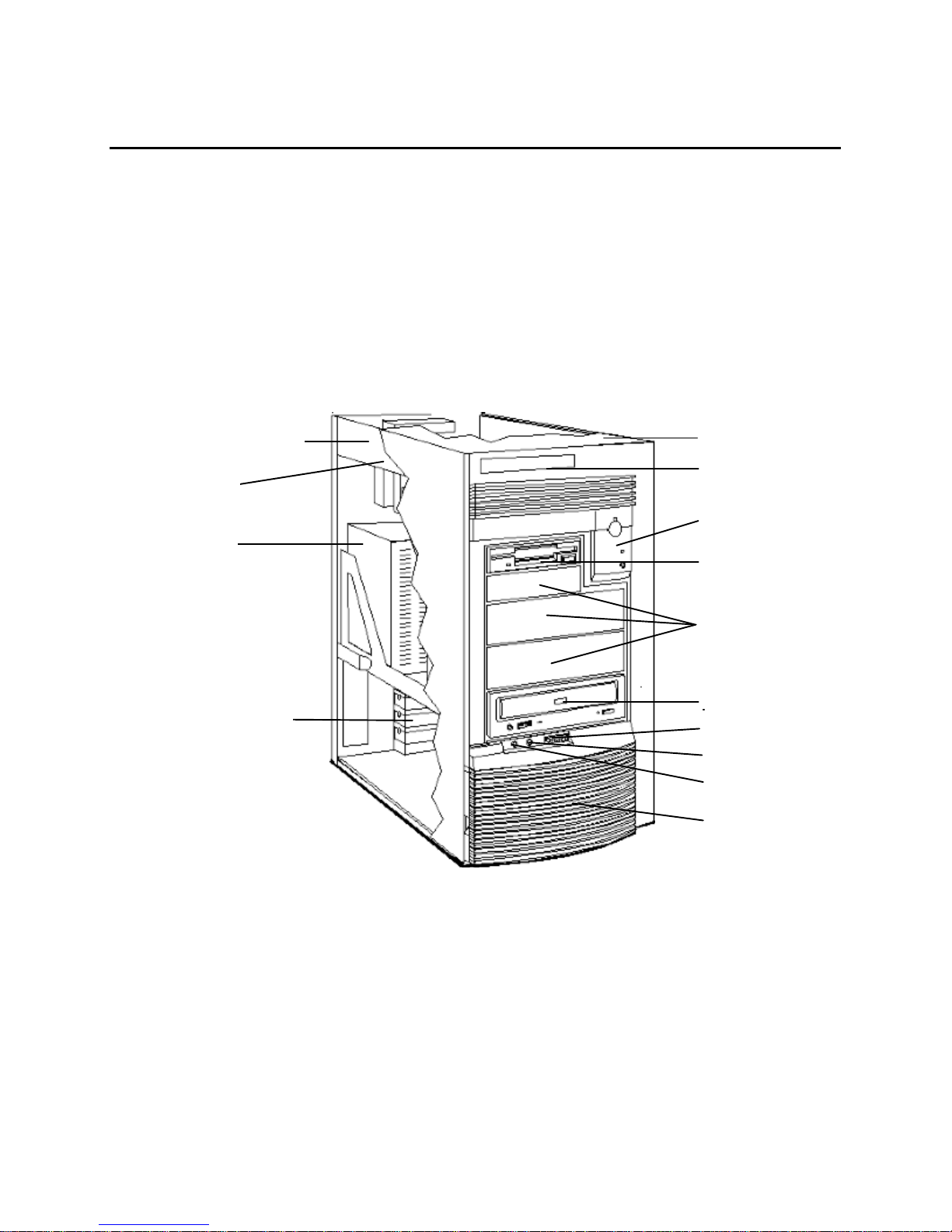
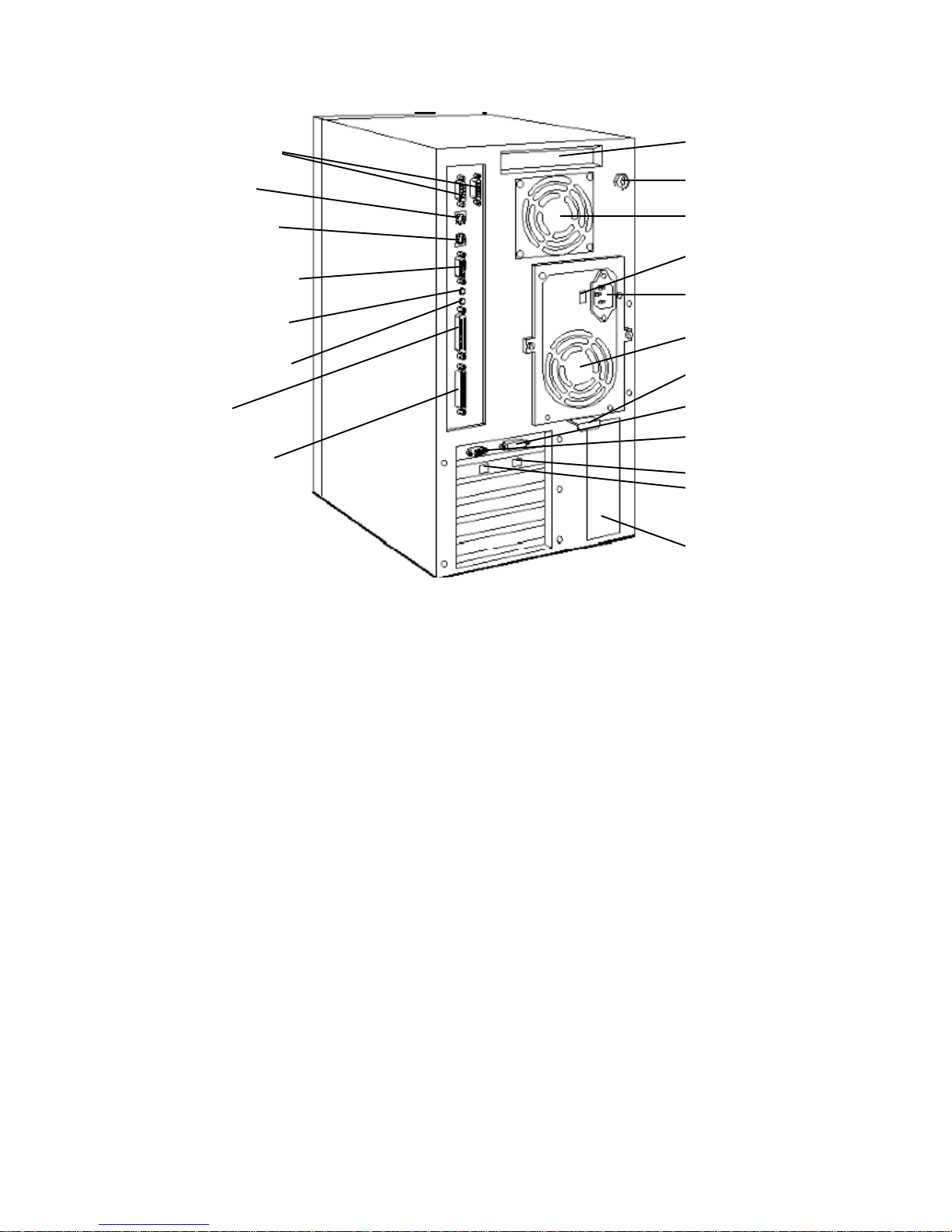
The following two diagrams show the front and rear views of the
“A” model network board. The
HP Vectra VT 6/xxx PC
is similar, but has no SCSI or LAN
connectors.
Empty internal drive shelf
HP Vectra XU 6/xxx PC
Main memory
Logo
Status panel
Flexible disk drive
Empty front access
drive shelves
with an
Up to six accessory
boards can be installed
CD-ROM drive
Volume control
Headphone jack
Microphone jack
Internal speaker grill
Page 7
Mouse connector
Serial ports B and A
Hand-hold recess
Key lock
Keyboard connector
MIDI/joystick connector
Stereo-in (audio) jack
Stereo-out (audio) jack
Parallel port
Fast-20 SCSI-2
connector (XU only)
INTERNAL FEATURES
Processor fan
Voltage selection
switch
Power connector
Power supply fan
Power supply handle
VESA connector
Display connector
100 Mb/s LAN
10 Mb/s LAN
(XU with "A" model
network board only)
Identification label
Both models of PC are constructed around the Peripheral Component Interconnect (PCI) bus and
Industry Standard Architecture (ISA) bus. They are the first members of the HP Vectra PC family
to use the Intel Pentium Pro (P6) processor.
Since there is no back-plane, the system board diagram, at the beginning of the next chapter,
shows the locations of all the PC’s main field-serviceable components. The components of the
system board are described in Chapter 2; the characteristics of the PC’s video, disk and
networking devices are described in Chapter 3. The HP BIOS routines are described in Chapter 4;
and the Power-On Self-Test routines are summarized in Chapter 5.
SPECIFICATIONS AND CHARACTERISTIC DATA
Status (Control) Panel
The status (control) panels of the
HP Vectra XU 6/xxx PC
following features:
• a power on/off button with integrated on/error status light
press-and-hold
• a
RESET button
• a hard disk activity light.
and
HP Vectra VT 6/xxx PC
have the
Page 8
PHYSICAL CHARACTERISTICS
System Processing Unit
Weight: 33 lbs (15 kg)
Dimensions: 15.95 inches (D) by 8.27 inches (W) by 16.34 inches (H)
(40.5 cm by 21 cm by 41.5 cm)
Footprint: 0.91 sq ft (0.085 m2)
Keyboard: 18 inches (W) by 7 inches (D) by 1.3 inches (H), when flat, or
18 inches (W) by 7 inches (D) by 2 inches (H), when standing
(464mm by 178mm by 33mm when flat, or
464mm by 178mm by 51mm, when standing)
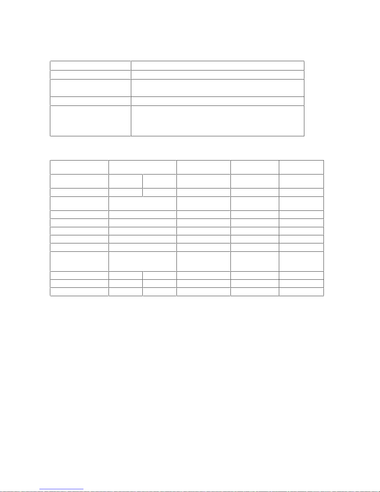
ELECTRICAL SPECIFICATION
Parameter Total Rating Notes
Input voltage 100-127
Vac
Input current (max) 6 A 3.15 A
Input power (max) 280 W Less than 5 W
Input frequency 47 Hz to 63 Hz
Heat dissipation 280 W
Available power 200 W 15 W (max) 15 W (max)
Max current at +12 V 4 A — 0.2 A 0.2 A
Max current at -12 V 0.5 A — 0.2 A 0.5 A
Max current at +3.3 V 16 A Together, these two
Max current at +5V 29 A 1 A
Max current at -5V 0.2 A — — 0.2 A
Max current at +5Vst 70 mA — — —
200-240
Vac
Switch selectable
when turned off
must not exceed
145 W*
Typical per PCI
Accessory Slot
These must not
exceed 2.5 A
per slot
Typical per ISA
Accessory Slot
—
*Since 29 A at 5 V equates to 145 W, it follows that for every 1 A that is required from the 3.3V
supply, it is necessasry to reduce the 29 A limit on the 5 V supply by 0.66 A. For example, 3A
at 3.3 V plus a maximum of 27 A at 5 V, or 6 A at 3.3 V plus a maximum of 25 A at 5 V.
An attempt to draw too much current (such as a short circuit across edge-connector pins, or an
accessory board that is not suitable for these PCs), will cause the overload protection in the power
supply to be triggered, and the PC could fail to boot.
Page 9
ENVIRONMENTAL SPECIFICATIONS
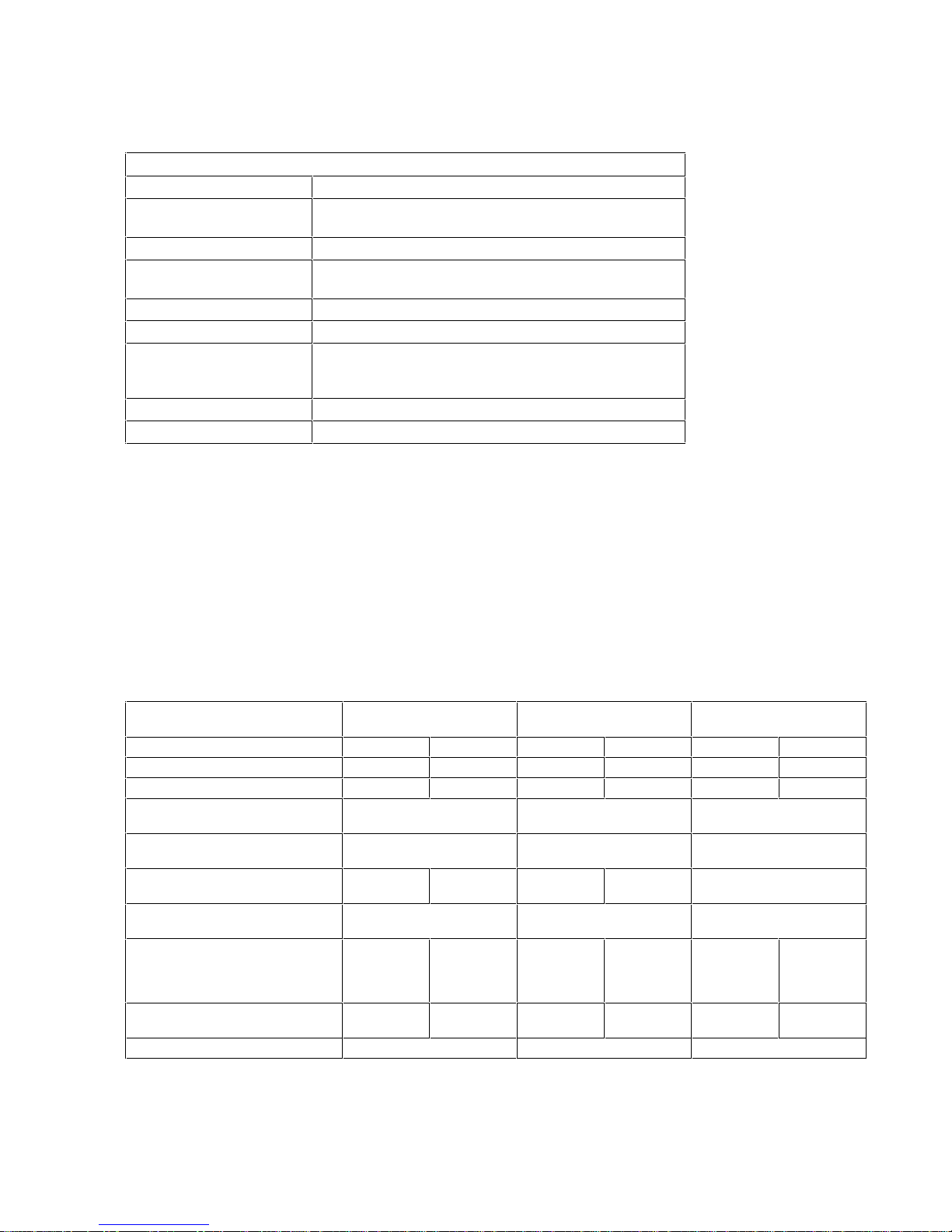
Environmental Specifications (System Processing Unit, with Hard Disk)
Operating Temperature + 40°F to 104° F (+5°C to +40°C)
Recommended
+59°F to +158°F (+15°C to +30°C)
Operating Temperature
Storage Temperature -40°F to +158°F (-40°C to +70°C)
Over Temperature
+122°F (+50°C)
Shutdown
Operating Humidity 15% to 80% (relative)
Storage Humidity 8% to 80% (relative)
Acoustic noise emission less than 40 dB in the workplace under normal
conditions as defined by DIN 45635 T.19 and ISO
7779
Operating Altitude 10000 ft (3100m) max
Storage Altitude 15000ft (4600m) max
Operating temperature and humidity ranges may vary depending upon the mass storage devices
installed. High humidity levels can cause improper operation of disk drives. Low humidity levels
can aggravate static electricity problems and cause excessive wear of the disk surface.
DOCUMENTATION
The table below summarizes the availability of the documentation that is appropriate to the
and
Vectra XU 6/xxx PC
HP Vectra VT 6/xxx PC
. Three dots, ‘...’, are used to indicate ‘XU’ or ‘VT’,
HP
as appropriate.
Only selected publications are available in paper-based form. Most are available as printable files
from the HP regional support servers, or from the
Title
Line of HPVectra 6/xxx PC: X U VT XU VT XU VT
HP Vectra ... 6/xxx User’s Guide yes yes yes yes D3538A D3539A
Optimizing Performance Guide yes no yes no no
HP Vectra XU/VT 6/xxx
Familiarization Guide
HP Vectra XU/VT 6/xxx Technical
Reference Manual
HPVectra PC Service Handbook
(9th Edition)
HPVectra Accessory Service
Handbook (5th Edition)
Network Administrators Guide WinHelp,
HP 10/100 VG Selectable PC LAN
Adapters
Matrox MGA Millennium no no* no
Regional Support
Servers
yes yes D3538-90901
yes yes no
yes yes yes yes 5963-8033
yes yes 5963-8034
HTML and
text
formats
yes not
Support Assistant
not
applicable
applicable
Support Assistant
yes not
yes not
CD-ROM.
CD-ROM Paper-based
applicable
applicable
no not
applicable
5963-2665 not
applicable
*Available on the XU/VT Drivers and Documentation CD-ROM
Page 10
WHERE TO FIND THE INFORMATION
Introducing the PC
Product features
Product model
numbers
Using the PC
Connecting cables
and turning on
Finding on-line
information
Environmental
Formal documents
Upgrading the PC
Opening the PC
Supported
accessories
Installing
accessories
Configuring
devices
Fields and their
options within
Setup
Repairing the PC
Troubleshooting
Technical
information
System board
BIOS
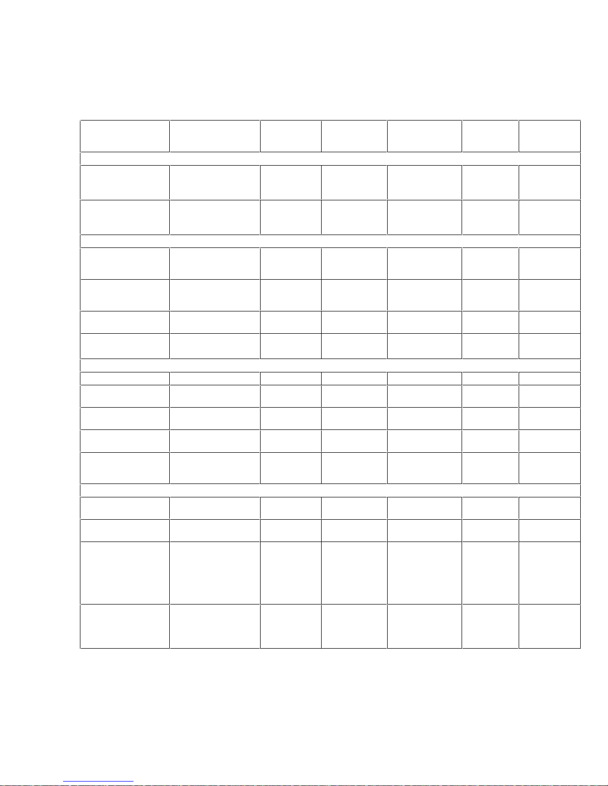
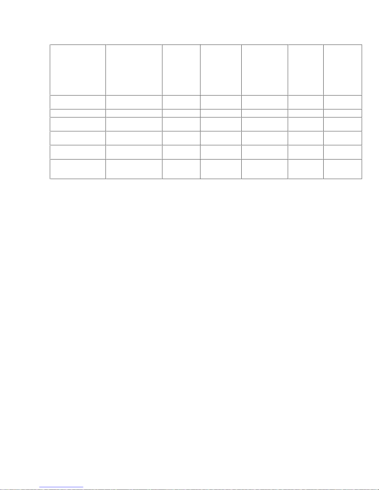
The table below summarizes the availability of information within the documentation:
User Guide User Online
Key features Exploring New features
Keyboard, mouse,
display, network,
printer, power
Finding READ.MEs
and on-line
documentation
Setting up the PC Working in
License agreement
Warranty information
Full details
Full PN details Full PN details Full PN
How to install Why to install New procedures
comfort
License
agreement
Performance
Guide
Familiarization
Guide
Vectra PC
comparison
Product range Product
Service
Handbook
Exploded
view
Parts list
range
CPL dates
details
Technical
Reference
Manual
Key features
Product
range
Installing drivers Configuring
Key fields New fields Complete
Basic Repair policy Service
Basic Advanced Basic Advanced
Jumpers, switches
and connectors
Basic details New features Technical
peripherals
Jumpers,
switches and
connectors
How to replace
notes
Jumpers,
switches
and
connectors
list
Advanced
Jumpers,
switches
and
connectors
Chip-set
details
details
Memory
maps
Page 11
Power-On Self-
Test routines
(POST)
Key error codes and
Vectra diagnostic
utility
Peripheral Devices
Display User’s
Guide
Disk drive User’s
Guide
Audio User’s
Guide
LAN
Administrator’s
Guide
suggestions for
corrective action
Setting up and
configuring
Setting up and
configuring
Setting up and
configuring
Setting up and
configuring
New features Error codes
and
suggestions
for
corrective
action
Order of
tests
New features Technical
details
Page 12
2 SYSTEM BOARD
The next chapter describes the video, disk and network devices which are supplied with the PC.
This chapter describes the components of the system board. An overview of the system board is
first given. Then the components of the Processor-Local Bus, the PCI Bus and the ISA Bus are
described in more detail.
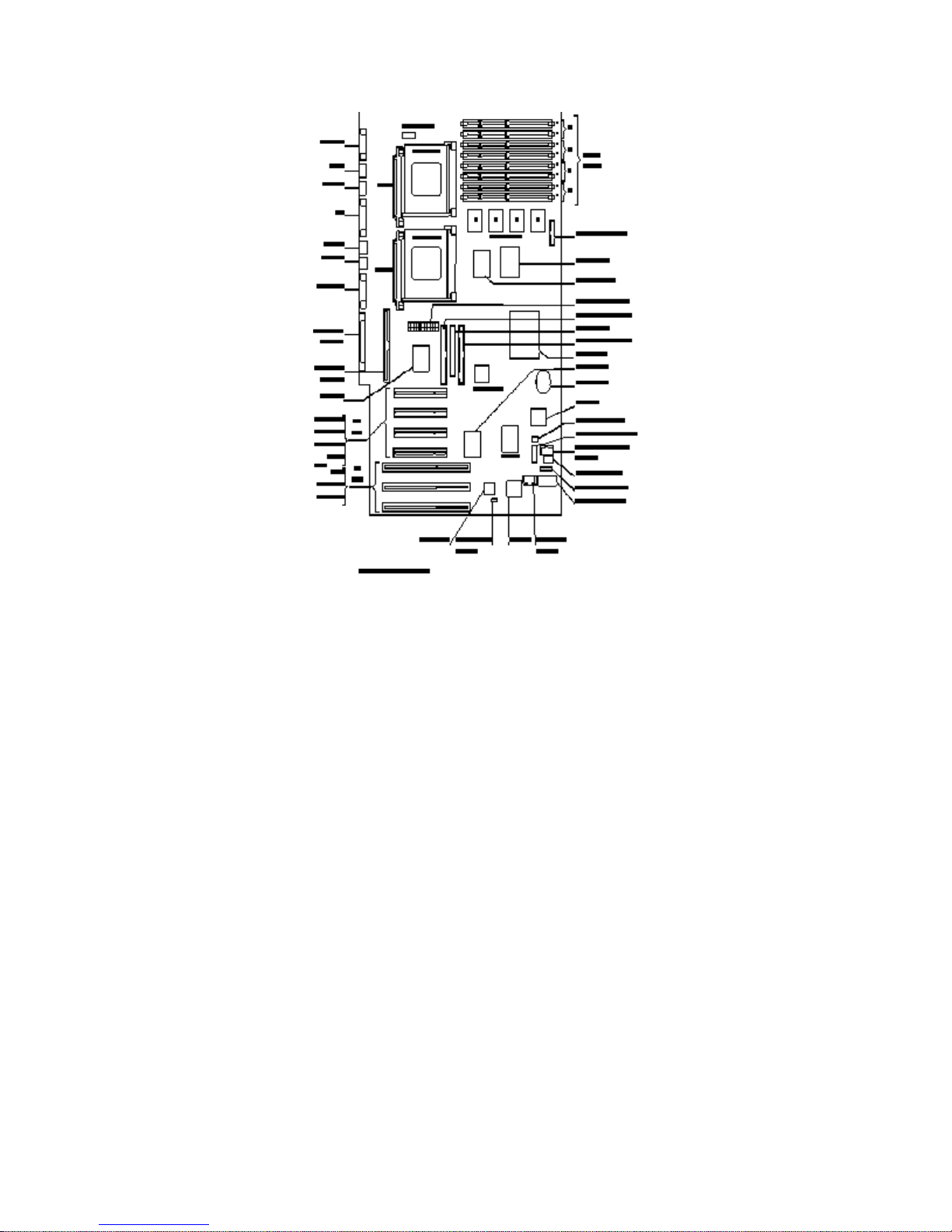
PRINCIPAL COMPONENTS AND FEATURES
The system board contains the following components:
PGA ZIF sockets
Each processor is packaged in a 387-way
board in a
zero-insertion-force
(ZIF)
socket
pin-grid-array
. The
HP Vectra XU 6/xxx PC
(PGA), which is seated on the system
has two such sockets: the
top one is occupied by the Pentium Pro (P6) processor; the bottom one is empty, and can be filled
with an optional second Pentium Pro processor. The
HP Vectra VT 6/xxx PC
has one socket,
occupied by the Pentium Pro processor, with no option for fitting a second Pentium Pro processor.
VRM sockets
voltage regulator module
The
(VRM) is capable of supplying a voltage of 1.5 V to 3.5 V. This
voltage is selected automatically, and depends on the needs of each processor. For instance, the
150 MHz Pentium Pro requires 3.1 V, whilst the 200 MHz version requires 3.3 V. There are two
VRM sockets on the
HP Vectra XU 6/xxx PC
HP Vectra VT 6/xxx PC
.
(one of which is already occupied), and one on the
Accessory Slots
There are three
accessory slots
on the PCI bus, two on the ISA bus, and one that lies on either
bus. Thus there are four PCI accessory sockets, and three ISA bus accessory sockets. The top
PCI bus slot is already occupied by the Matrox MGA Millennium video controller. On the
HP Vectra XU 6/xxx PC
, the second PCI slot is also already occupied, by the HP PCI Integrated
10/ 100 VG Interface. (These two boards are described in the next chapter).
System Board Switches
The first three of the
system board switches
set the configuration for the PC, as summarized in the
table below. The next two set the frequency of the Processor-Local bus, and the last three the ratio
of processor-frequency to Processor-Local-bus-frequency.
Switch: Function: OFF (default) ON
1 - CONFG Retain or clear the configuration which is stored in EEPROM Retain Clear
2 - PSWRD Enable or clear the User and System Administrator Passwords
3 - SECURE Security mode prevents changes to the PC’s configuration with
4, 5, 6, 7, 8 Processor bus frequencies (see the table on page 15)
which are stored in EEPROM
Setup
the
program
Enable Clear
Disable Enable
Page 13
Wavetable Interface Connector
This is used when installing a Creative Labs wavetable accessory board that operates with the
integrated SoundBlaster audio interface.
Main Memory Module Sockets
There are eight
main memory module sockets
already occupied by the pair of
double interline memory modules
, arranged in four banks(A to D). One bank is
(DIMMs) that contain the 16 MB
of memory that is fitted as standard on all models of the PC.
SCSI Controller and Connector
Ultra SCSI controller
An
, on PCI bus of the
HP Vectra XU 6/xxx PC
, supports
Fast-20 SCSI-2
.
Internal and external connectors are provided.
IDE Controller and Connector
The Enhanced IDE (EIDE) controller chip can be found next to the IDE connectors. Connected to
the PCI bus, it has IDE-Master capability. It has two channels, each capable of supporting two
devices: a primary channel (recommended for EIDE, or IDE, hard disk drives, using the grey
connectors); a secondary channel (recommended for EIDE, or IDE, CD-ROM drives, using the red
connectors).
Page 14

Ultra I/O Chip
The
Ultra I/O
chip is located just slightly above and to the right of the ISA slots. It is a combined
controller on the ISA bus for the flexible disk drive connector, and for the one parallel and two
serial communications ports.
Audio Chip
SoundBlaster 16
The
chip is located to the right of the Ultra I/O chip, near the bottom right hand
edge of the board. This provides the audio interface, and is driven from the ISA bus.
Chip-Set
Intel 82450KX chip-set
The
comprises eight chips. Six of them are concerned with controlling
memory accesses, and are located below the memory module sockets. These are the four
datapath units, the memory controller chip, and the Mem/PL bridge chip. They are described in the
sub-section of this chapter entitled “Main Memory”. The remaining two chips are the PL/PCI bridge
chip, which is described in the section entitled “Devices on the PCI Bus”, and the PCI/ISA bridge
chip, which is described in the section entitled “Devices on the ISA Bus”.
Gold Capacitor
Gold Capacitor
A
is provided instead of a battery, and can store enough energy to power the
CMOS configuration memory for over a week after the mains power has been disconnected.
Architectural View
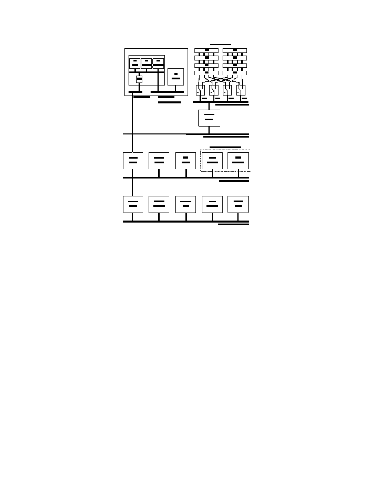
The following block diagram gives an architectural view of the
HP VectraXU 6/150 PC
. The next
section describes the devices on the system board which are associated with the Processor-Local
(PL) bus. The section after describes the devices on the system board that are associated with the
Peripheral Component Interconnect (PCI) bus. The final section describes the devices on the
system board that are associated with the Industry Standard Architecture (ISA) bus.
Page 15
DEVICES ON THE PROCESSOR-LOCAL BUS
The following subsystems are associated with the Processor-Local bus:
• Intel Pentium Pro (P6) microprocessor
• cache memory
• optional second microprocessor (
• main memory.
HP Vectra XU 6/xxx PC
only)
INTEL PENTIUM PRO (P6) MICROPROCESSOR
Apart from the two levels of cache memory, contained within the processor’s single integrated
package, the other new features of the Pentium Pro are:
• three-way super-scalar pipeline (versus two for the Pentium)
• five execution units (versus three for the Pentium)
• 12 stage super-pipeline (versus 5 stage pipeline for the Pentium)
• dynamic, out-of-order, speculative execution
• 16-state, dynamic multiple branch prediction
• split-transaction bus
• register renaming.
Although it is not pin compatible with the Pentium, the Pentium Pro is backward code-compatible.
Software written for previous HP Vectra models will run on the Pentium Pro-based HP Vectras.
However, only 32-bit programs execute faster. 16-bit programs might even only execute at the
speed that would have been attained by an equivalent 80486-based system.
Page 16
Many techniques have been adopted to accelerate the throughput of the instruction-pipeline of the
Pentium Pro over that of the Pentium. Firstly, it is
super-pipelined
: the individual operations of the
Pentium pipeline have been broken down into many sub-operations, leading to a much longer
pipeline of smaller operations. Secondly, it is
super-scalar
: the five execution units are completely
independent; not only can they have instructions issued to them asynchronously of each other, but
they can complete their execution asynchronously of each other, too.
Since instructions can complete asynchronously, it is possible for a simple instruction to complete
before a complex one which precedes it. This is the first of two ways in which the Pentium Pro
manifests
out-of-order instruction execution
speculative execution
feature: whilst a time-consuming instruction is still awaiting completion, the
. The second way follows as a direct result of the
processor gets on with executing instructions that were fetched after it, on the speculation that they
will probably be needed next.
Related to this, the Pentium Pro incorporates an even more elaborate (and more accurate) 16-
dynamic branch prediction
state
mechanism than the one which is used on the Pentium. This
allows the processor to speculate as to which instructions will be needed following a conditional
branch, based on past behavior at the branch.
A module, known as the
re-order buffer
(ROB), handles the out-of-order completion of instructions,
and the cases where speculative execution proves to have been wrong (a misprediction by the
branch prediction unit, for example).
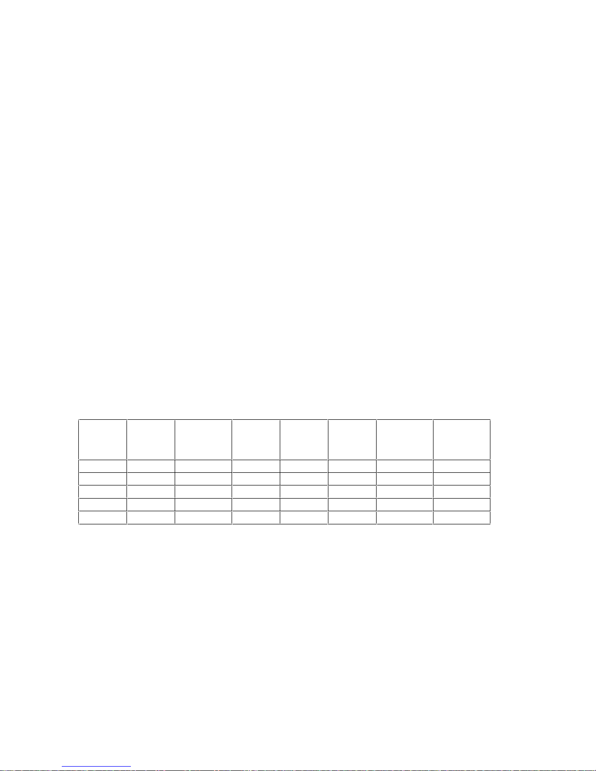
System Board Switch Speed Settings
Like the Pentium and 80486 DX2 processors, the Pentium Pro uses internal clock multiplication.
For example, the Pentium Pro 150 MHz processor multiplies the 60 MHz system clock by 2.5.
Switches 4 and 5 on the system board switch bank set the frequency of the Processor-Local bus.
Switches 6, 7 and 8 set the clock multiplier ratio. The relationship of the switch settings to
Processor-Local bus and processor frequencies is summarized in the following table:
Switch 4 Switch 5 Processor
Local Bus
Frequency
Off Off 66 MHz Off Off Off 2 : 1 133 MHz*
On Off 60 MHz On Off Off 2.5 : 1 150 MHz
Off Off 66 MHz On Off Off 2.5 : 1 166 MHz
On Off 60 MHz Off On Off 3 : 1 180 MHz
Off Off 66 MHz Off On Off 3 : 1 200 MHz
*The 133 MHz PentiumPro processor is not supplied in any of the Vectra models. This information is
provided for completeness only.
Switch 6 Switch 7 Switch 8 Frequency
Ratio
Processor :
Local Bus
Processor
Frequency
CACHE MEMORY
There are two integrated circuits sealed within a single Pentium Pro package. One of these
contains the Level-2 (L2) cache memory chip; the other contains the processor, which includes two
banks of Level-1 (L1) cache memory.
Each L1 cache memory has a capacity of 8 KB, and is set-associative. The L2 cache memory has
a capacity 256 KB, and is four-way set-associative.
Data is stored in the cache memories in lines of 32-bytes (256 bits). This involves two consecutive
transfers of 128-bits with the main memory.
Page 17

The Pentium Pro processor guards against
cache coherency
problems by monitoring the accesses
to the memory which are made by other PC devices (including DMA controllers, and a second
processor, if installed) through a mechanism known as
MESI
line are two status bits which define the
state (modified, exclusive, shared or invalid) of the
bus snooping
. Associated with each cache
cache line.
The amount of cached memory is set by Intel, at the time of manufacture, so cannot be changed.
It is anticipated that Intel will offer new versions of the Pentium Pro (P6) processor with 512 KB of
L2 cache memory. Upgrading the processor will then become possible as the means for changing
the amount of cache memory.
Extending the amount of cache memory can never have a detrimental effect on the performance.
can
However, it
experience a law of diminishing returns, so that extending the cache memory does
not have a cost-effective impact on the performance. Finding the correct amount to install is an
empirical process, either by simulation, or by trial and error on the real hardware.
PROCESSOR-LOCAL BUS
The Processor-Local bus of the
HP Vectra XU 6/150 PC
and
HP Vectra VT 6/150 PC
is 64 bits
wide, and is clocked at 60 MHz. Although carrying 64-bits of data, it is in fact composed of 141
signals. These are implemented using Intel’s GTL+ technology. To reduce voltage over- and
under-shoots, the signals are clamped to a 0 to 1.5 voltage range (with 60 mA per signal), and are
filtered to prevent the logic edges from becoming too steep (that is, there is a minimum constraint
on the rise and fall times, as well as the usual maximum constraint).
The bus is implemented as a
split-transaction bus
. A device (such as the Pentium Pro processor)
can send a request (such as asking for the contents of a given memory address) and, rather than
waiting for the result, it can release the bus, to get on with other work. The target device then
requests the bus when it is ready to respond, and sends the requested data packet. Up to eight
transactions are allowed to be outstanding at any given time.
OPTIONAL SECOND MICROPROCESSOR
The support of Intel's
the integrated L2 cache (which dispenses with the need for a proprietary bus to communicate
among processors) ideally suits the Pentium Pro for the construction of multiprocessor systems.
As many as four of them can be directly connected together, without the need for extra glue logic.
At present, however, the
Not all operating systems support a second processor. Of those that do, not all uses of them
increase the performance. Installing a second processor is only advantageous when the software
can make use of parallel activity. In particular, you need to be running a multi-threaded operating
system that supports multiprocessing (one that is
Solaris, OS/2 SMP and Windows NT. Of these, the Windows NT operating system makes best use
of the Pentium Pro’s 32-bit architecture (though other operating systems will also show some
benefit if 32-bit application programs are run). This is covered in the
Performance on the HP Vectra XU 6/xxx PC
Advanced Priority Interrupt Controller
HP Vectra XU 6/xxx PC
only allows for dual processing capability.
MPS-ready
, and is summarized in the following table.
(APIC), the split-transaction bus, and
), such as SCO-Unix, NextStep,
Guide to Optimizing
SCO
Unix
Multi-threaded Yes Yes Yes Yes Yes Yes No No
MPS-ready Yes Yes No No Yes No No No
32-bit operating
system
Yes Yes Yes Yes Yes Partial* No No
Next
Step
Sunsoft
Solaris
OS/2 Windows NT
3.5 (or greater)
Windows95Windows
3.x
DOS
Page 18

32-bit applications
available
*32-bit operation at the outermost levels, but only 16-bit working internally
**With the 32S library
Yes Yes Yes Yes Yes Yes Partial** No
The two processors must be operating at the same bus speed and the same processor speed, with
the switch settings set accordingly, otherwise erroneous operation will result.
MAIN MEMORY
The
HP Vectra XU/VT 6/xxx PCs
DRAM.
The modules are organized in pairs so that a request for a transaction to or from the L2 cache
memory will cause two consecutive blocks of 16 bytes (128 bits) to be accessed. Rather than
accessing all 128 bits simultaneously, the 64-bit data bus is used more efficiently by
two accesses, the first to one half of the memory bank (for example, A1/B1/C1/D1), the second to
the other (for example, A2/B2/C2/D2).
Although each memory module stores a line of 64 bits of data (8 bytes), each ECC memory
module of the
HP Vectra XU 6/xxx PC
bus. The extra bits are generated by the Mem/PL Bridge chip, and are used to implement the
correcting code
(ECC). A subsequent error in a memory bit can be corrected, by referring to these
extra bits, and hence neither causes the data to be lost, nor corrupted, nor the computation to be
aborted (as would have been the case with simple parity detection, as on the
).
PC
use
fast page-mode
(FPM) DRAM, not
extended data-out
is, in fact, serviced by a 72-bit Intel proprietary memory
HP Vectra XU 5/xx
(EDO)
interleaving
error
Chip-Set Chips that are involved in Memory Access
The Mem/PL Bridge chip (OMC-DP) is an Intel 82452KX. It interfaces between the ProcessorLocal (PL) bus, whose datapath is 64-bits wide, and the Intel proprietary memory bus, whose
datapath is 72-bits wide. During a memory-write operation, on the
HP Vectra XU 6/xxx PC
, the
chip generates 8 ECC parity bits. During a memory-read operation, the chip regenerates the 64
data bits from the 72-bit bus, applying error correction when appropriate.
Each of the four datapath chips (the Memory Interface Chips, MIC) is an Intel S82451KX, and acts
as a two-way switch, able to connect alternately to the A1,B1,C1,D1 side of the interlaced
memory, or the A2,B2,C2,D2 side. Since only an 18-bit path can be handled, four units are
needed. Datapath units 1, 2, 3 and 4, handle bits 0..17, 18..35, 36..53 and 54..71, respectively.
Finally, the memory controller chip (OMC-DC) is an Intel S82453KX. It is responsible for decoding
the signals on the address and control paths from the Processor-Local (PL) bus, and for generating
the appropriate control signals for the memory banks (such as RAS, CAS, WE# and the address
lines).
Error Correcting Code Operation
HP Vectra XU 6/xxx PC
The
can tolerate as many as one faulty memory bit per 64-bit line of
instruction or data words. The erroneous bit is corrected (automatically and transparently) by the
hardware. The computer program continues to execute as if no error had occurred.
If two, or more, bits are faulty within any given 64-bit line, the effect is the same as it would have
been without error correction. The effect of executing a faulty instruction is always unpredictable,
and might cause the program to ‘hang’. The effect of reading a faulty data word is often similarly
Page 19

unpredictable, but can sometimes be tolerated (for instance, it might merely appear as a corrupted
pixel on a video display).
HP Vectra XU 6/xxx PC
The
as standard. The banks can be filled in any order, up to a maximum capacity of 256 MB, but
always in pairs of memory modules of the same capacity and same type (ECC or non-ECC). Only
HP Vectra XU 6/xxx PC
the
disabled if any non-ECC memory is installed. Conversely, the
16 MB and 32 MB ECC modules, but will treat them as non-ECC memory.
Setup
The
or non-ECC) is installed in each bank.
Extending the capacity of main memory, and upgrading it with faster chips, can never have a
detrimental effect on the performance. However, it
that upgrading the memory does not have a cost-effective impact on the performance. Finding the
correct combination is an empirical process, whether it be through simulation, or by trial and error
on the real hardware.
program automatically detects which memory module capacity, speed, and type (ECC
and
HP Vectra VT 6/xxx PC
supports ECC (error correcting code) memory, but even this will be
are supplied with 16 MB of main memory
HP Vectra VT 6/xxx PC
can
experience a law of diminishing returns, so
will accept
DEVICES ON THE PCI BUS
The PL/PCI bridge chip (OPB) is an Intel S82454KX. It is responsible for transferring data between
the Processor-Local bus and the PCI bus. It also houses the controller for the PCI bus.
• Fast-20 SCSI-2 interface (
• IDE controller
• other devices in the PCI accessory slots, including:
• video controller
• LAN controller.
HP Vectra XU 6/xxx PC
only)
SMALL COMPUTER SYSTEM INTERFACE (SCSI)
An Adaptec AIC-7880 controller is integrated on the
implements Fast-20 SCSI-2 (also known as Ultra-SCSI). It attains data transfer rates up to 20 MB
per second on 8-bit wide data, single-ended. It supports up to seven SCSI devices, with a choice
of internal and external SCSI connectors. The external SCSI connector is on the rear panel.
An HP provided driver is required for the OS/2 2.11 and Windows NT operating systems; an
HP provided driver is also recommended for the Windows 3.11, Windows 95 and OS/2 Warp
Connect operating systems.
SCSI-configured-automatically (SCAM) support is provided at level 1, for Plug and Play.
HP Vectra XU 6/xxx PC
system board. It
INTEGRATED DRIVE ELECTRONICS (IDE)
The CMD646 chip supports Enhanced IDE (EIDE) and Standard IDE. To use the Enhanced IDE
features, though, hard disk drives must be compliant with Enhanced IDE.
Up to four IDE devices can be supported: two connected to the primary channel cable, and two to
the secondary channel cable. With EIDE, it is possible to have a fast device, such as a hard disk
drive, and a slow device, such as a CD-ROM, on the same channel without affecting the
performance of the fast device. The BIOS automatically sends a command to auto-detect each
drive, and thereby select, automatically, the fastest configuration that is supported by it. However,
in general, the primary channel cable (the grey one) is recommended for hard disk drives, and the
secondary channel cable (the red one) for CD-ROM drives.
Page 20
Transfer Rates Versus Modes of Operation
Bytes per
Sector
512
512
512
The controller supports 32-bit Windows and DOS I/O transfers (many IDE controllers use Windows
integral IDE driver which only supports 16-bit I/O transfers). It has PCI master capability, and
supports programmed I/O (PIO) modes up to mode 4 and direct memory access (DMA) modes up
to mode 2 (giving a cycle time of 120 ns, and a transfer rate of 16.7 MB per second, in both
cases). The five PIO modes allow the following transfer rates:
Mode 0 1 2 3 4
Cycle time (ns) 600 383 240 180 120
Transfer rate (MBytes/s) 3.33 5.22 8.33 11.1 16.7
The three DMA modes allow the following transfer rates:
Mode 0 1 2
Cycle time (ns) 480 150 120
Transfer rate (MBytes/s) 4.2 13.3 16.7
Operated in SLAVE mode, the IDE controller saturates the PCI bus with transfers, thus limiting the
actual achieved transfer rate to 4 or 5 MBytes per second. Operated in MASTER mode, though,
the IDE controller is allowed to work autonomously of the CPU, and the full 16.7 MBytes per
second transfer rate can be achieved, with less than 33% occupancy of the PCI bus (so allowing
the CPU to get on with other work for more than 67% of the cycle times, whilst the IDE transfers
are going on in parallel).
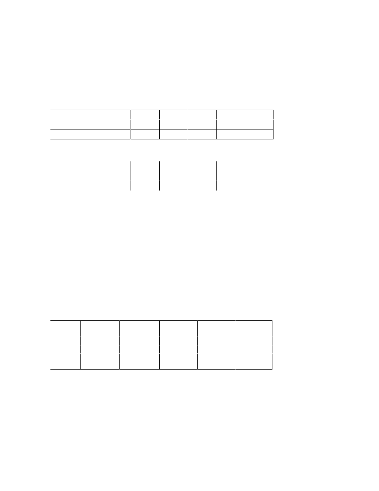
Disk Capacity Versus Modes of Addressing
The amount of addressable space on a hard disk drive is limited by three factors: the physical size
of the hard disk, the addressing limit of the IDE hardware, and the addressing limit of the BIOS.
The Extended-CHS addressing scheme allows larger disk capacities to be addressed than under
CHS, by performing a translation (for example regrouping the sectors so that there are twice as
Setup
many logical tracks as is possible under the CHS addressing scheme). If the
field has been
set to automatic, the logical block addressing (LBA) mode will be selected for each device that
supports it.
Cylinders
per Device
CHS 64 16 1024
ECHS 64 256 1024
LBA - - 256 M
Heads per
Cylinder
Sectors
per Track
(=228)
Bytes per
Device
528 M
8.4 G
137 G
OTHER PCI ACCESSORY DEVICES
PCI accessory boards are for high-speed peripheral accessories. There are four slots on the PCI
bus for accessory boards. One of these is already occupied by the video controller board, and a
second (on the
HP Vectra XU 6/ xxx PC
chapter. The fourth slot is a combination slot with the ISA bus.
) by the LAN board; these are described in the next
Page 21

Plug and Play
Plug and Play is an industry standard for automatically configuring the PC’s hardware. When you
start the PC, the Plug and Play system BIOS can detect automatically which hardware resources
(IRQs, DMAs, memory ranges, and I/O addresses) are used by the system-based components.
HP Vectra XU/VT 6/xxx PC
The
Required” level for Plug and Play. Accessory boards which are Plug and Play are automatically
configured by the BIOS (Windows 3.11) or by the operating system (Windows 95).
Error Diagnostics and Suggested Corrective Actions
Most problems caused by incompatibilities on PCI accessory boards are detected by the POST
during the Power-On sequence. This is described in Chapter 5.
s have a “PnP level 1.0A” BIOS and meets the “Windows 95
DEVICES ON THE ISA BUS
The PCI/ISA bridge chip (otherwise known as the system I/O chip, SIO-A) is an Intel S82379AB. It
is responsible for transferring data between the PCI bus and the ISA expansion bus. It also houses
the controller for the ISA bus, and incorporates the logic for a DMA interface, a DMA controller
that supports fast DMA transfers, data buffers to isolate the PCI and ISA buses, Timer/Counter
logic, APIC, and NMI control logic.
• Ultra I/O controller, containing the following:
• serial / parallel communications ports
• flexible drive controller (FDC)
• real time clock (RTC) and CMOS memory
• keyboard and mouse controller
• serial EEPROM
• Little BEN
• audio controller
• System ROM
• other ISA accessory devices.
ULTRA I/O CONTROLLER
Serial / parallel communications ports
The Ultra I/O chip (SMC 37C932) supports two serial ports and one bidirectional multi-mode
parallel port. The two 9-pin serial ports (on the rear panel) support RS-232-C and are buffered by
16550 UARTs, with 16 Byte FIFOs. They can be programmed as COM1, COM2, COM3, COM4, or
disabled.
The 25-pin parallel port (also on the rear panel) is Centronics compatible, supporting IEEE 1284. It
can be programmed as LPT1, LPT2, or disabled. It can operate in the following modes:
• Standard mode (PC/XT, PC/AT, and PS/2 compatible).
• Bidirectional mode (PC/XT, PC/AT, and PS/2 compatible).
• Enhanced mode (enhanced parallel port, EPP, compatible).
• High speed mode (MS/HP extended capabilities port, ECP, compatible).
FDC
The flexible drive controller (FDC) is software and register compatible with the 82077AA, and
100% IBM compatible. It has an A and B drive-swapping capability and a non-burst DMA option. It
Page 22

supports the D2035B, 3.5-inch, 1.44 MB flexible disk drive.It is software compatible with the
DP8473, the 765A, and the N82077. It has a 16-byte FIFO, though this is disabled by default. It
supports burst and non-burst modes. It provides perpendicular recording drive support. It has a
high-performance internal digital data separator (no external filter components are required). It is
implemented in low-power CMOS technology.
RTC
The real-time clock (RTC) is 146818A-compatible. The configuration RAM is implemented as 256
bytes of CMOS memory.
Serial EEPROM
Setup
This is where the default values for the
Keyboard and Mouse Controller
program are held.
HP Vectra XU 6/xxx PC
The
mouse controller.
and
HP Vectra VT 6/xxx PC
have an 8042-based keyboard and
LITTLE BEN
Little BEN is an HP application specific integrated circuit (ASIC) that contains the following:
• hard and soft control for the power supply
• BIOS timer
• flash access and protection
• Ultra I/O protection
• programmable chip selects
• glue logic
AUDIO CONTROLLER
The
HP Vectra XU 6/xxx PC
SoundBlaster 16 audio interface integrated on the system board. This has the following
specification:
• 80 dB SNR
• 8-bit and 16-bit stereo sampling from 5 kHz to 44.1 kHz
• Yamaha FM OPL3 synthesizer (11 polyphonic voices)
• connector for WaveBlaster standard (wave-table synthesizer) board
• 3 inputs (1 microphone, 1 stereo-in, 1 CD-ROM)
• 3 outputs (1 internal speaker, 2 stereo-out capable of supporting low-impedance headphones)
• connector for MIDI /joystick interface (MPU-401 UART compatible).
and
HP Vectra VT 6/xxx PC
have a Creative Labs Vibra 16S CT2504
The headphones jack, microphone jack, and volume control are each on the front panel; the MIDI
socket, stereo-in (audio) jack and stereo-out (audio) jack are each on the rear panel. The
microphone input has an input impedance of 600 ohms and a sensitivity of 30 mV (peak-to-peak)
to 200 mV (peak-to-peak). The headphones jack and the stereo-out (audio) jack each supply 2 W
per channel into a 4 ohm load, and can thus be used interchangeably.
The Windows 95, OS/2 and Windows NT operating systems each have integrated drivers
Creative SoundBlaster 16
(
Menuet
of HP
drivers.
). The DOS and Windows 3.x operating systems require the installation
Page 23

SYSTEM ROM
The System ROM consists of 256 KB of 200ns, Flash EEPROM, implemented within a single 256
K 5 8-bit ROM chip. This is a ROM that is returned to its unprogrammed state by the application of
appropriate electrical signals to its pins, and hence can then be reprogrammed with the latest
upgrade firmware.
The System ROM contains the LAN boot firmware, and the system BIOS (including the boot code,
Setup
the ISA and PCI initialization, the
error messages). These are summarized in Chapters 4 and 5.
Updating the System ROM
The System ROM can be updated with the latest BIOS firmware. This can be ordered from HP or
downloaded from one of HP’s online services. (For more information on HP’s online services, refer
to the Hewlett-Packard Support and Information Services chapter in the User’s Guide that was
supplied with the computer.)
The System ROM is updated by running the HP6Init utility (HP6INIT.EXE) which is supplied with
BIOS upgrade. The procedure for doing this is given in the
computer.
program and the Power-On Self-Test routines, plus their
User’s Guide
that is supplied with the
You must specify the
cannot be used with this one. It must be run from diskette. Do not switch off the computer until the
system BIOS update procedure has completed, successfully or not, since irrecoverable damage to
the ROM may be caused. While updating the flash ROM, the power supply switch and the reset
button are disabled to prevent accidental interruption of the flash programming process.
Error Diagnostics and Suggested Corrective Actions
The programs and data in the system ROM are accompanied by a check-sum code. If any of the
programs or data ever become corrupted, the check-sum will no-longer correspond with the
contents of the ROM, and the appropriate part of the POST routine will attempt to report the error:
model number
of the PC since the utility which supplied for a different model
Cannot display error messages
Flash ROM may be defective
The suggested corrective action is to reprogram the system ROM by running the same
utility as is normally used for upgrading it.
HP6Init
OTHER ISA ACCESSORY DEVICES
ISA accessory boards are for slow peripheral accessories. There are three slots on the ISA bus for
accessory boards. One of these is a combination slot with the PCI bus.
Plug and Play
All PCI accessory boards are Plug and Play, although not all ISA boards are. Check the accessory
board’s documentation if you are unsure.
The procedure for installing an ISA accessory board that is not Plug and Play in Windows 3.11 or
Windows 95 is described in the
User Guide
that is supplied with the PC.
Page 24

Error Diagnostics and Suggested Corrective Actions
Most problems caused by incompatibilities on ISA accessory boards are detected by the POST
during the Power-On sequence. This is described in Chapter 5.
Page 25
3 INTERFACE BOARDS AND MASS-STORAGE
DRIVES
This chapter describes the video, disk and network devices which are supplied with the PC. These
include the Matrox MGA Millennium video
controller board, and the HP PCI Integrated 10/100 VG Interface. It also includes the hard disk
drives, flexible disk drives and CD-ROM drives that are supplied with the PC.
Matrox MGA Millennium Video Controller Board
All models are supplied with a Matrox MGA Millennium PCI video controller on a board fitted in a
PCI accessory slot. This controller has an MGA-2064W processor, 2 MB video memory installed
on the board, a VESA feature connector, and a socket for either a video memory upgrade module
or an MPEG upgrade module. The possible upgrades for this socket are the following:
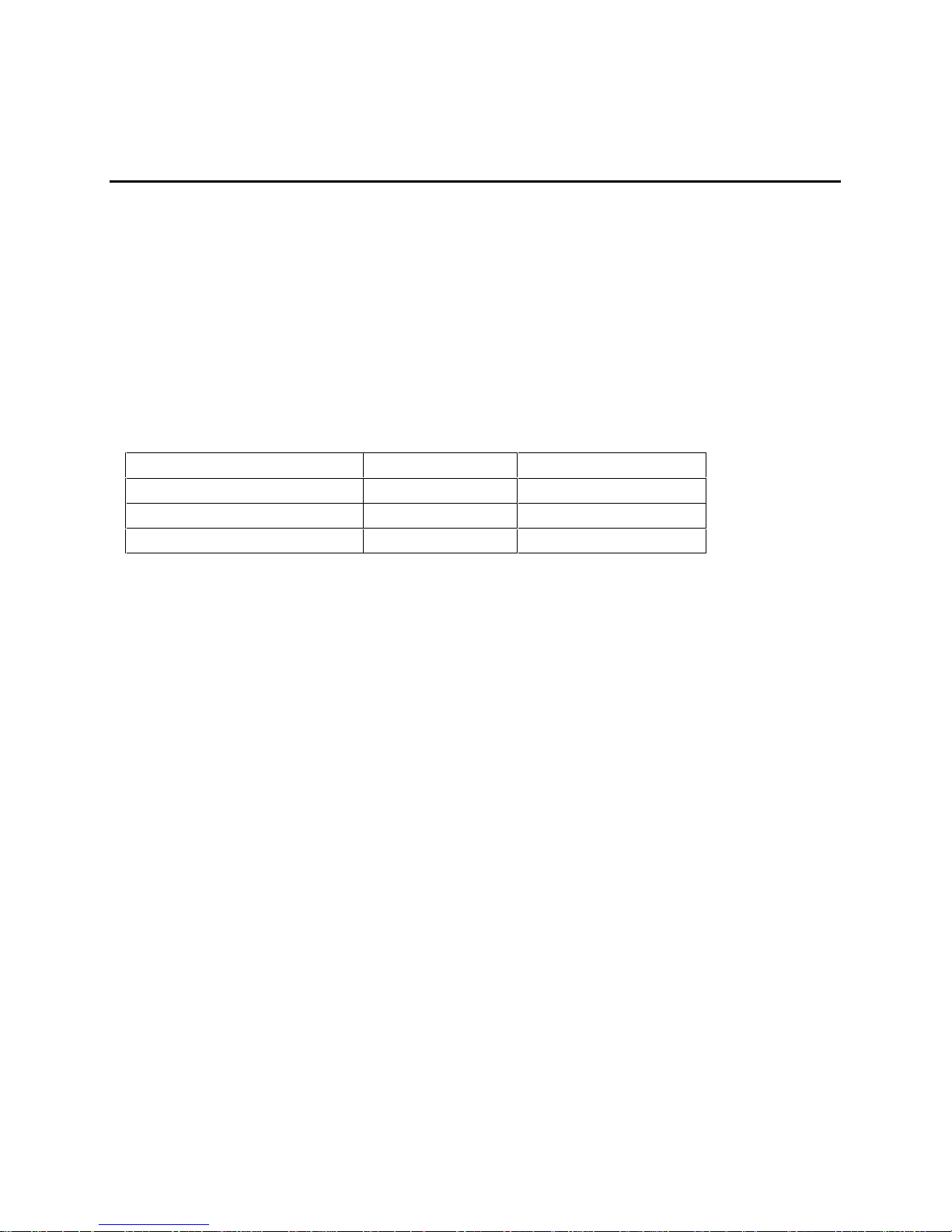
Add on module HP Part Number Matrox Part Number
2 MB video memory module D3557A MGA-MIL/MOD2
6 MB video memory module not available MGA-MIL/MOD6
MPEG module not available MGA-MIL/Media-XL
The video RAM (also known as window RAM, or WRAM) is a local block of RAM for holding two
major data structures: the double buffer (to hold one frame steady on the screen whilst the next
one is being processed), and the Z-buffer (for storing depth information for each pixel). It is dual
ported, so that it can be inputting and outputting simultaneously.
The controller uses the PCI bus for data transfers between the processor and the video
subsystem, and has the following features:
• 100% compatible with IBM
• 64-bit video memory access
• Hardware acceleration of graphical user interface (GUI) operations
• Support for up to 8 MB Video RAM (Window RAM) at 60 ns
• Graphics resolutions of up to 1600 5 1200
• Integrated 24-bit, 175 MHz RAMDAC
• Pixel clock maximum frequency of 135 MHz
• Green PC power saving features
• Standard and Enhanced Video Graphics Array (VGA) modes
• DDC 2B compliant.
Drivers are not integrated into any of the operating systems, so HP-provided drivers must be
installed.
® VGA display standard
AVAILABLE VIDEO RESOLUTIONS
If you attempt to set the resolution or number of colors higher than is supported by the installed
video memory, the screen refresh rate is lowered automatically, and image flicker becomes more
noticeable. If the resolution/ refresh-rate combination is set higher than the display can support,
you risk damaging the display.
Page 26
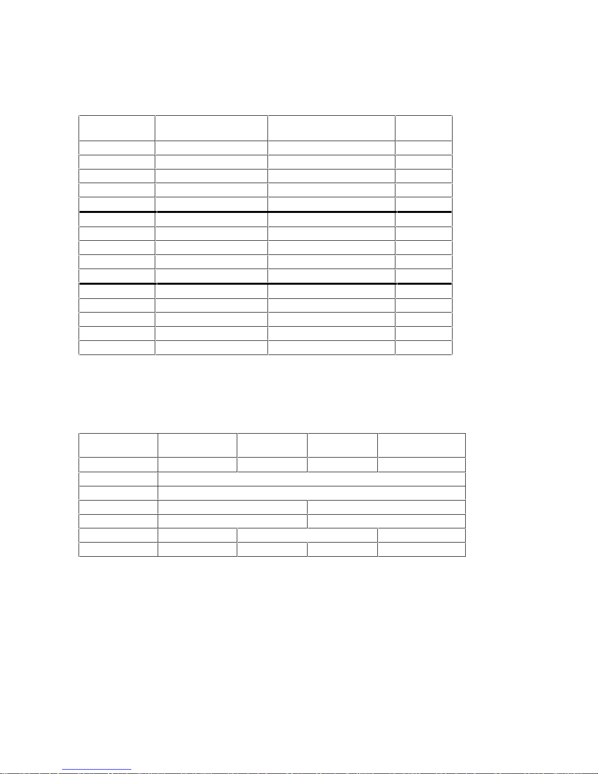
The number of colors supported is limited by the graphics card and the video RAM. The
Resolution
640 x 480
800 x 600
1024 x 768
1280 x 1024
1600 x 1200*
640 x 480
800 x 600
1024 x 768
1280 x 1024
1600 x 1200*
640 x 480
800 x 600
1024 x 768
1280 x 1024
1600 x 1200*
16.7 M
True-Color
32
8 MB, 100 Hz
Not supported
resolution/refresh-rate combination is limited by a combination of the display, the graphics card,
and the video RAM.
Number of colors Video Adapter Maximum
Refresh Rate (Hz)
256, 64K, 16M 120 2 MB
256, 64K, 16M
256, 64K
256 100
256 72
256, 64K, 16M 120 4 MB
256, 64K, 16M
256, 64K, 16M
256, 64K, 16M (24 bpp) 100
256, 64K 72
256, 64K, 16M 120 8 MB
256, 64K, 16M
256, 64K, 16M
256, 64K, 16M 100
256, 64K, 16M 72
*The upper limit of refresh rate for HP monitors is 60Hz at this resolution.
Memory
The table below summarizes the video resolutions which are supported. However, SCO Unix only
supports 15 BPP, instead of 16 BPP, and does not support 32 BPP; OS/2 does not support 24
BPP.
Number of
Colors 256
Bits per Pixel
640 x 480 2 MB, 120 Hz
800 x 600 2 MB, 120 Hz
1024 x 768 2 MB, 120 Hz 4 MB, 120Hz
11x2 x 882 2 MB, 100 Hz 4 MB, 100 Hz
1280 x 1024 2 MB, 100 Hz 4 MB, 100 Hz
1600 x 1200* 2 MB, 72 Hz 4 MB, 72 Hz 8 MB, 72 Hz
*The upper limit of refresh rate for HP monitors is 60Hz at this resolution.
81624
64 K
Hi-Color
16.7 M
True-Color
Page 27
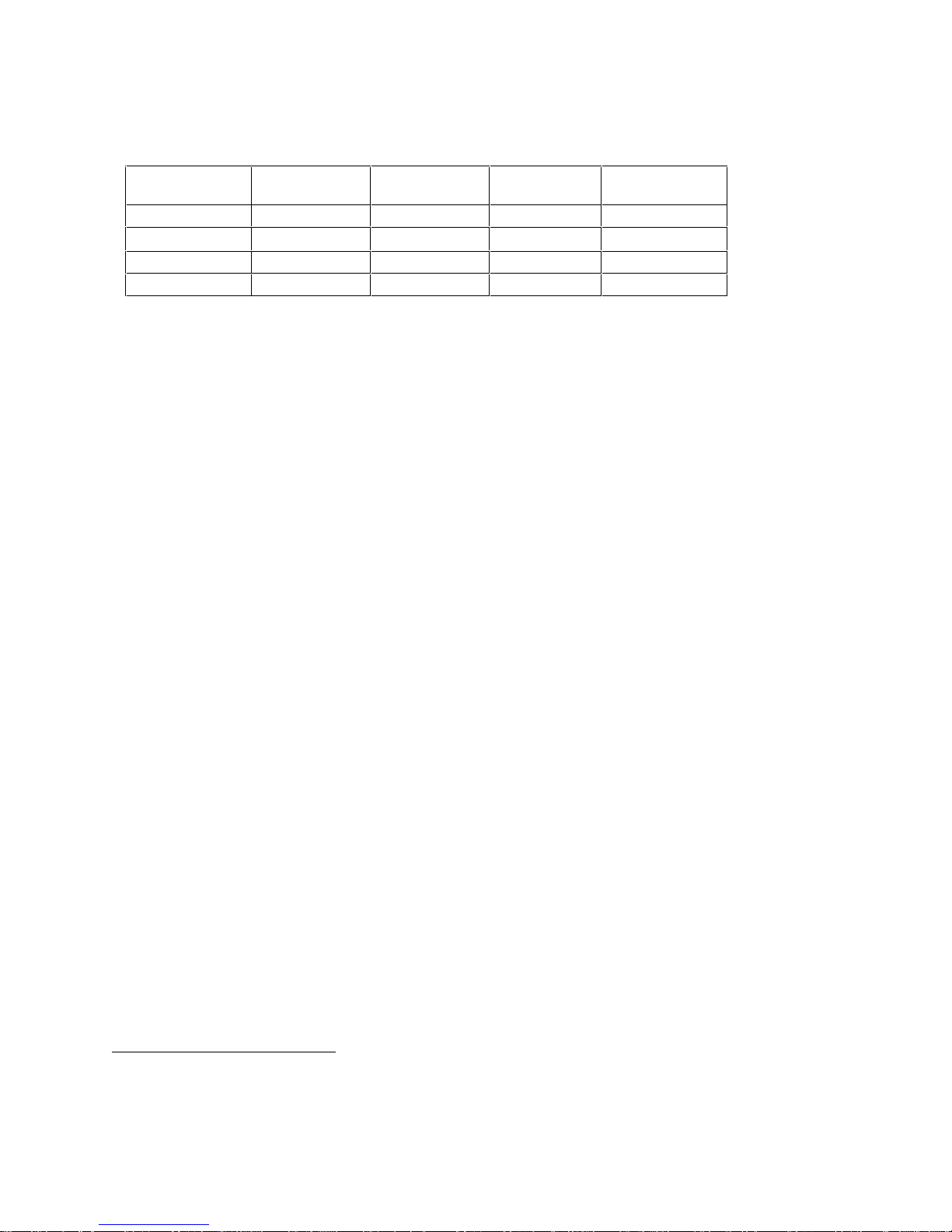
The maximum 2D resolutions for any given video memory capacity and color scale can be found
from the following table:
Number of
Colors
Bits per Pixel 8 16 24 32
2 MB 1600 x 1200
4 MB 1600 x 1200 1600 x 1200 1280 x 1024 11x2 x 882
8 MB 1600 x 1200 1600 x 1200 1600 x 1200 Not supported
256 64 K
Hi-Color
1024 x 768
16.7 M
True-Color
1
800 x 600 800 x 600
16.7 M
True-Color
VESA CONNECTOR
The Video Electronics Standards Association (VESA) defines a standard video connector,
variously known as the VESA
feature
The Matrox MGA Millennium video adapter board supports an output-only VESA
connector,
auxiliary
connector, or
pass-through
feature
connector.
connector
in VGA mode. This connector is integrated on the adapter board, and is connected directly to the
pixel data bus and the synchronization signals.
VIDEO BIOS
Tables that detail the standard VGA modes which are currently implemented in the video BIOS
can be found in the
Documentation
Matrox MGA Millennium Adapter
CD-ROM that is supplied with the computer.
The capability to flash program the video BIOS is a feature of the Matrox MGA Millennium board.
This is achieved as follows:
documentation, on the
XU/VT Drivers and
1 Set SW-1, on the Matrox board, to ON (BIOS unprotected).
Setup
2 Set the “Operating System” field in the
program to Others.
3 Run the video BIOS flash program, progbios.exe, and the associated *.bin file, which are
provided by HP.
4 Set SW-1, on the Matrox board, to OFF (BIOS protected).
Setup
5 Set the “Operating System” field in the
program back to an appropriate setting.
Video boards without ROM (such as old CGA and monochrome) are not supported by the BIOS.
Memory holes above 1 MB are not supported. DDC display detection is not a BIOS feature, but is
handled by the video drivers.
ERROR DIAGNOSTICS AND SUGGESTED CORRECTIVE ACTIONS
Further help can be found in the
Drivers and Documentation
For more information on the Matrox MGA Millennium video adapter board, contact Matrox
Electronic Systems.
Matrox MGA Millennium Adapter
documentation, on the
CD-ROM that is supplied with the computer.
XU/VT
Page 28
Matrox Electronic Systems Ltd.1055 St. Regis Blvd.
Dorval, Quebec
Canada H9P 2T4
Telephone: (514) 685-2630
Fax: (514) 685-2853
BBS: (514) 685-6008
HP PCI INTEGRATED 10/100 VG INTERFACE
The HP PCI Integrated 10/100 VG Interface is supplied in a PCI accessory slot of the
XU 6/xxx PC
100 VG-AnyLAN, 100 Mbits per second over voice grade cable (IEEE 802.12 standard for
Ethernet); 10 BaseT, 10 Mbits per second, ISO 8802-3 (IEEE 802.3 standard).
On the rear panel there are either one or two RJ-45 unshielded-twisted-pair (UTP) connectors.
One is for 100 Mbits per second and the other for 10 Mbits per second, or else they are both
combined in a single connector. The D2746A Coaxial Adapter accessory is available for users who
require a BNC coax connector. There are four lights for monitoring the adapter status, as
summarized in the following list:
• Activity light, showing network activity
• Link status light
• 100 Mbit/s light
• 10 Mbit/s light.
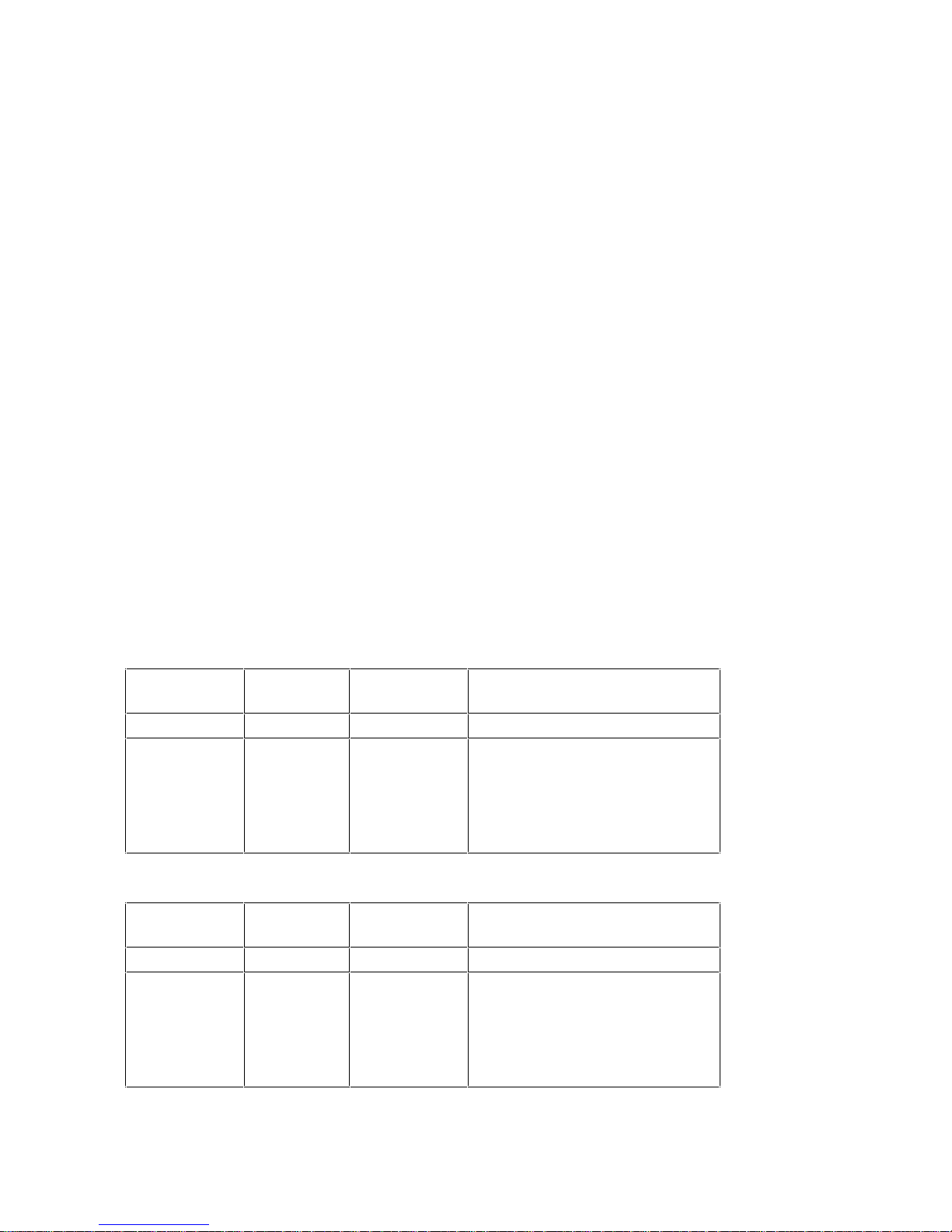
The following tables summarize the meanings of the various combinations of these lights being
illuminated:
. Both the A model and B model of this interface support the following two standards:
HP Vectra
10-Mbits/s Operation
Link Status
Light
ON ON OFF Normal operation
OFF OFF ON Either:
10-Mbits/s
Light
100-Mbits/s
Light
Explanation
Cable is not connected to an
active 10BaseT network.
Cable is defective.
LAN Adapter is defective.
100-Mbits/s Operation
Link Status
Light
ON OFF ON Normal operation
OFF OFF ON Either:
10-Mbits/s
Light
100-Mbits/s
Light
Explanation
Cable is not connected to an
active 100VG network.
Cable is defective.
LAN Adapter is defective.
Page 29
For the temporary storage of data received or awaiting transmission over the network, the A model
2 GB IDE
D2928A
Seagate
Cyclone
ST32140A
10 ms
4500
5.6 ms
16.7 MB/s
256 KB
has a 128 KB
packet buffer
. The B model has a 32 KB packet buffer.
The new, enhanced
demand priority access
(DPA) protocol guarantees access to any end node
that requests to transmit, while ensuring priority access to end nodes that require consistent, and
thereby, continuous access for applications such as full-motion video or video conferencing. This
protocol, through being collisionless with priority allocation, allows you to minimize unused
capacity on your network, and so maximizes network throughput.
The A model can be configured completely by software (no switches or jumpers need changing).
The controller can be I/O mapped or memory mapped: the fastest mode is automatically selected
by the driver. An HP provided driver needs to be installed within the operating system.
The B model is I/O mapped, and has Bus-Master capability.
HP Vectra XU 6/xxx PC
The
is supplied with a multi-protocol boot program integrated within the
System ROM, and has a complete LAN client drivers and diagnostics package (Microsoft client,
Novell client, IBM LAN server client and Warp connect, Banyans client, DEC pathworks client, all
major TCPIP stacks, Lantastic).
ERROR DIAGNOSTICS AND SUGGESTED CORRECTIVE ACTIONS
Diagnostic software, in the form of a DOS utility called
Drivers and Documentation
CD-ROM.
The LAN administrator’s guide (provided in ASCII, WINHELP and HTML format) is a useful source
of further information. The
HP 10/100 VG Selectable PC LAN Adapters Installation Guide
2665) contains detailed diagnostic information.
HPVGSet
, is provided on the
XU/VT
(5963-
MASS-STORAGE DRIVES
The SCSI and IDE controllers are described in chapter 2. The flexible disk controller is described
in chapter 2.
HARD DISK DRIVES
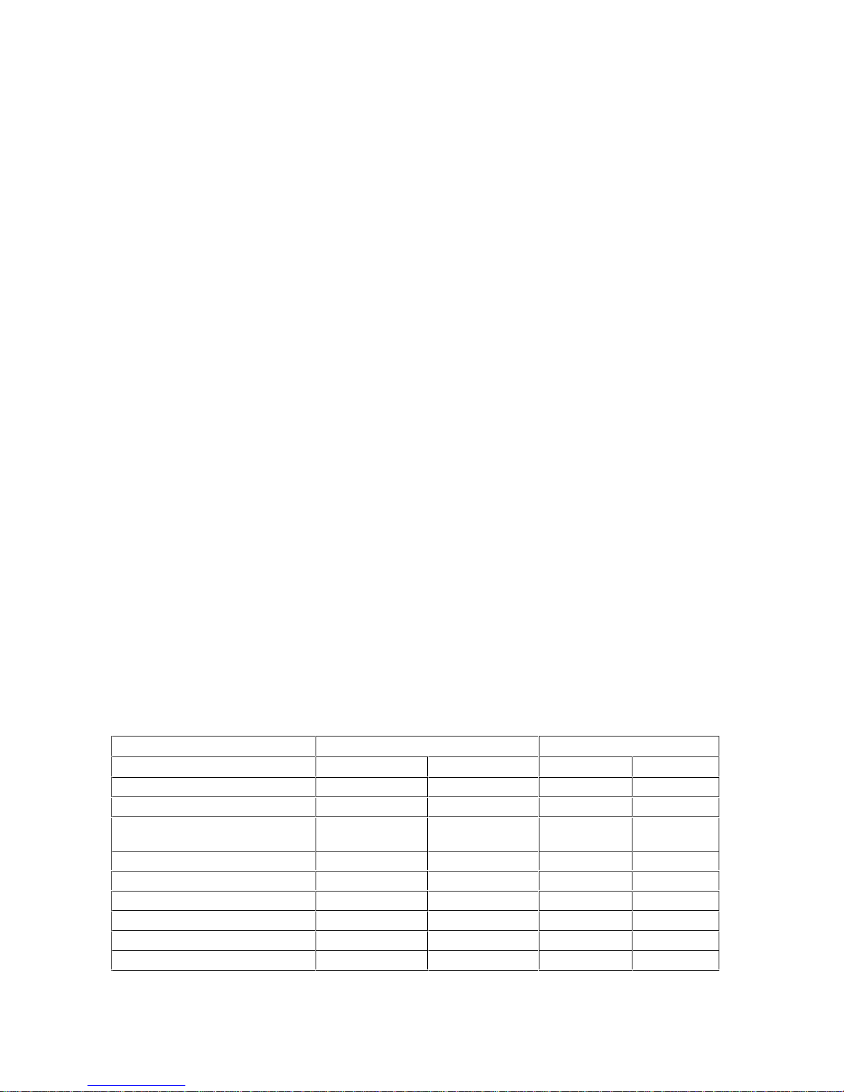
A 3.5-inch hard disk drive is supplied on an internal shelf in some models of the
6/xxx PC
HP product number D2926A D2920A
Manufacturer Seagate Quantum
Product name Barracuda 2LP
Average seek time 10 ms 12 ms
Revolutions per minute (RPM) 7200 5400
Average latency 4.2 ms 5.6 ms
Maximum transfer rate 10 MB/s 10 MB/s
Read/write cache memory size 480 KB 80 KB 80 KB
Buffer size 512 KB 128 KB
and the
HP Vectra VT 6/xxx PC
HP Vectra XU 6/xxx PC HP Vectra VT 6/xxx PC
2 GB SCSI 1 GB SCSI
ST32550N
.
Fireball 1080S
HP Vectra XU
1 GB IDE
D2919A
Quantum
Fireball
1080AT
12 ms
5400
5.6 ms
16.7 MB/s
128 KB
Page 30

FLEXIBLE DISK DRIVES
A 3.5-inch, 1.44 MB flexible disk drive (D2035B) is supplied on the top front-access shelf of all
models of the
HP Vectra XU 6/xxx PC
and the
HP Vectra VT 6/xxx PC
.
CD-ROM DRIVES
A D2992B quadruple-speed (45) SCSI CD-ROM drive is supplied on the bottom front-access shelf
HP Vectra XU 6/xxx PC
of the
A D2896B quadruple-speed (45) IDE CD-ROM drive is supplied on the bottom front-access shelf
HP Vectra VT 6/xxx PC
of the
.
.
Page 31

4 HP BIOS
The
Setup
program and BIOS are covered in the two sections of thischapter. The first section lists
Setup
the fields which are presented by the
options which are available. The second section lists the reserved addresses that are used by the
BIOS.
The POST routines are described in the next chapter.
program, describing the purpose of each, and the
SETUP
PROGRAM
You can interrupt the POST to run the
message appears on the initial “Vectra” screen.
The up and down arrows allow the cursor to be moved from one field to the next (also the left and
right arrows, when there is more than one field on the line). Pressing [F1] causes a “Help” screen
to appear, containing a more detailed description of what the field is for, and what the options are;
pressing [F1] again causes the “Help” screen to disappear again. Pressing [F8] causes the
contents of the field to be changed to the next available option, and pressing [F7] causes the
contents to be changed back to an earlier option. Pressing [F10] causes the page to be sent to the
printer port. Pressing [F3] causes a save and exit from the
causes an exit without updating the configuration.
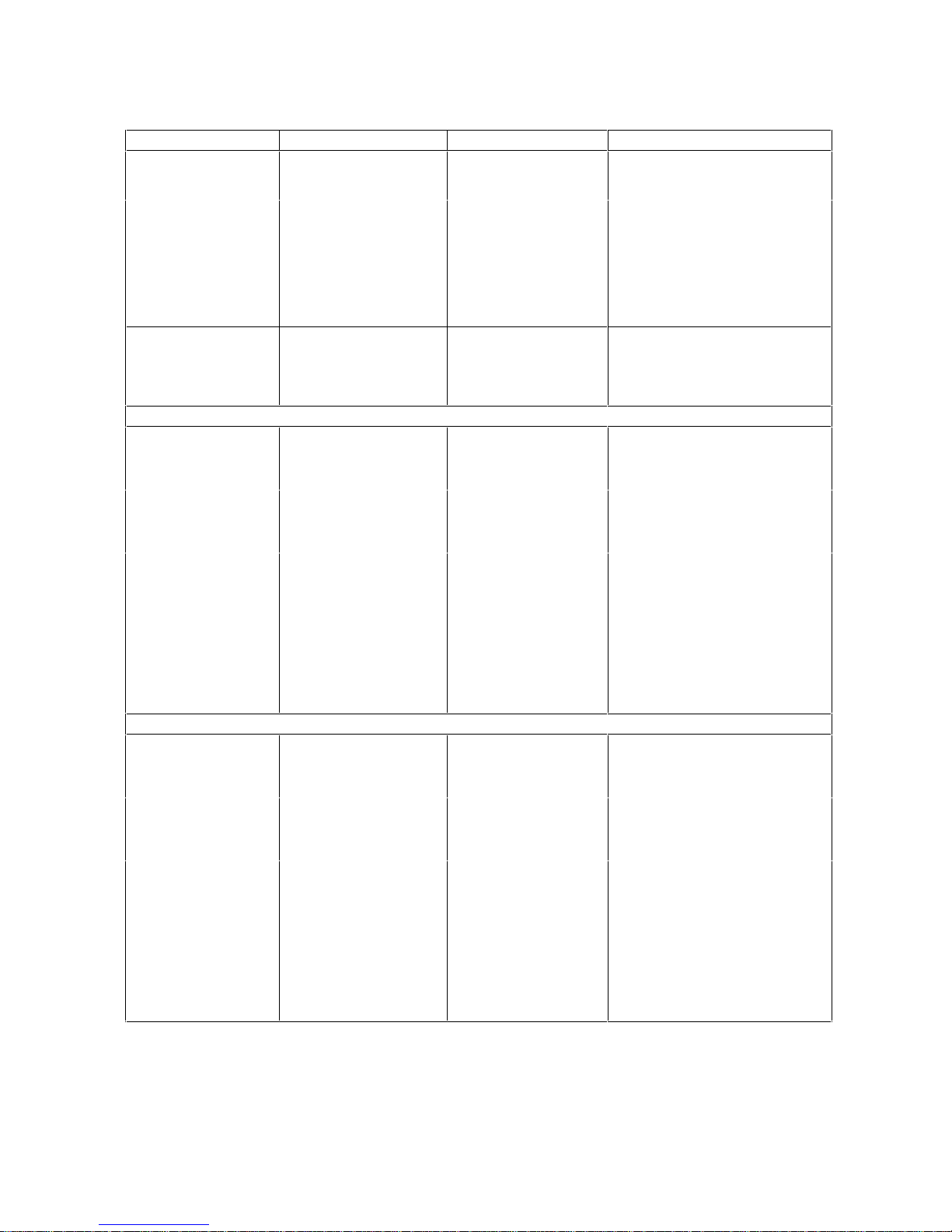
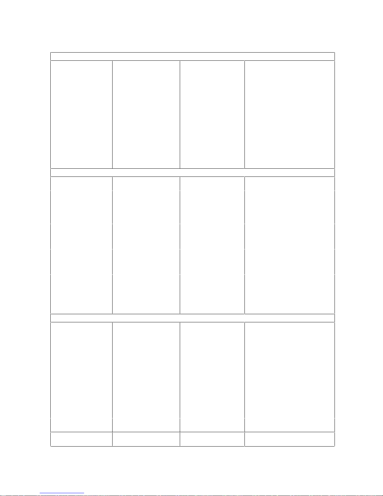
A complete list of fields, their meanings, and the options which are available, can be found on the
following pages. They include the following new features:
• A “Configuration Summary” screen.
• Within the “user preferences” section:
• An “operating system” field (for setting Windows 95, Windows NT, IBM OS/2 or Others)
• A “space-bar power on” field
• A “memory test” field (which can be set to disabled for fast boot).
• Two “IDE” sections, one for the primary channel, and one for the secondary channel. Within
each section, fields are provided to set (1) the use of two drives, (2) whether the transfer
speed is optimized or standard, and (3) whether the translation method is automatic, standard
CHS or extended CHS.
Setup
program by pressing [F2] when the F2=
Setup
program, and pressing [F12]
Setup
• A “start-up center” section, containing fields that allow the selection of boot device (FDD,
HDD, LAN). Booting from a SCSI device is possible in mixed IDE/SCSI configurations on the
HP Vectra XU 6/xxx PC
• An “audio” section, with fields that allow for the setting of addresses, IRQs, DMA channels.
You can scroll down through the fields using the down arrow key or the [PAGE DOWN] button.
Similarly, the up arrow key or the [PAGE UP] button can be used for going back to earlier fields in
the program.
Setup
The
fields. For instance, if Serial Port A is set to using IRQ4, then IRQ4 will not be offered as an option
for use when setting Serial Port B.
program is sufficiently intelligent as to not allow the user to set illegal settings within the
.
Page 32
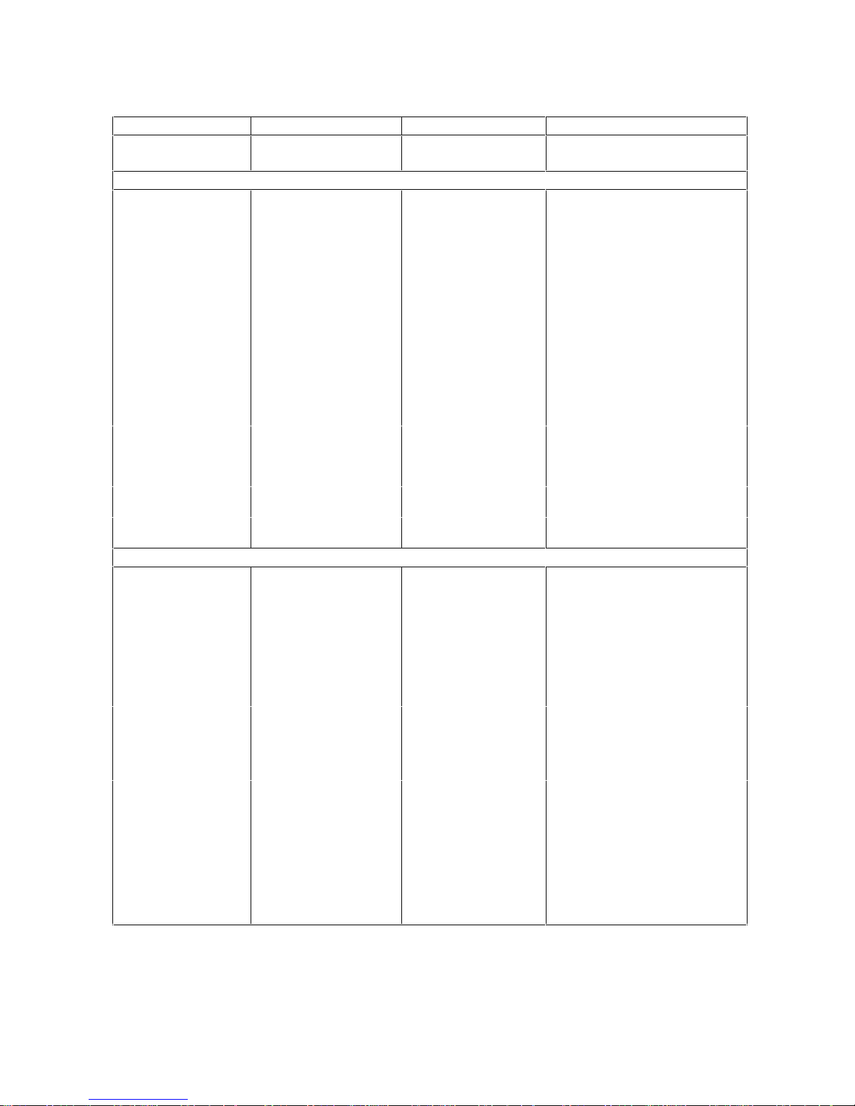
Field name Purpose Options Remarks
Date
Time
CONFIGURATION SCREEN
System BIOS Version Displays version number Cannot be change All of these are automatically
MILLENNIUM Video
Board
Processor Displays processor &
Memory Displays capacities Cannot be changed e.g. (16MB: 640KB Base, 384KB
IDE Hard Disk Drives Indicates if one is
LAN Interface Indicates MAC address if
USER PREFERENCES
Operating System Selects which operating
User Password Prevents unauthorized
Key Autorepeat Speed Sets the speed at which a
Delay Before
Autorepeat
Power-on NumLock
State
Space-bar Power On Allows the PC to be re-
Memory test Allows time to be saved
Sets the date
Sets the time
Displays type, memory
size, video BIOS and
version number
speed
detected
detected
system is to be run
access to your PC
key’s function repeats
Sets the delay before
which a key automatically
repeats its function
Sets whether the
NumLock key is enabled
when the PC is powered
on
activated by pressing the
space-bar
during a reset, by not
testing the main memory
YYYY/MM/DD
HH:MM:SS
detected, and cannot be changed
Automatically detected if the original
system board is present; else, if it
has been changed, the serial
number will be blank. It is possible to
use MS-DOS,
diagnostics without ti being set.
POST will detect no serial number
as an error. Follow the instructions
as they appear on the screen to
enter the new number; when
completed this will then appear on
future
Cannot be changed e.g. MILLENNIUM, 2.0MB, Version:
Cannot be changed e.g. (Processor: Pentium Pro,
Cannot be changed e.g. (No IDE disk detected)
Microsoft WINDOWS
95/
IBM OS2 /
Microsoft WINDOWS
NT/
Others
Set / Not set
2 to 30 per second
0.25 to 1 second
On / Off
Enabled / Disabled
Enabled / Disabled
838-7
150MHz)
Reserved, 15360KB Extended)
e.g. (MAC Address 08 00 09 A8 E5
82)
To set your password press
[ENTER]
type your password and press
[ENTER]
type your password and press
[ENTER]
again and the screen will show that
the password is set.
Setup
Setup
screens
and HP Vectra
Page 33
MEMORY SIZE
Base, on system board Confirms that
Base, on accessory
board
Base, TOTAL
Reserved
Extended
TOTAL Ensure that the TOTAL field is
Memory hole below
1 MB
IDE PRIMARY CHANNEL
Device 1 Defines the first primary
Device 2 Defines the second
Data Transfer Speed Sets between EIDE and
Translation Method Sets between CHS,
Primary Integrated
Channel
IDE SECONDARY CHANNEL
Device 3 Defines the first
Device 4 Defines the second
Data Transfer Speed Sets between EIDE and
Translation Method Sets between CHS,
Secondary Integrated
Channel
detected and configured
the memory size fields
Tells
location of any ISA
accessory boards which
are memory mapped
below 1 MB
IDE hard disk drive
primary IDE hard disk
drive
the original (older) IDE
protocol
ECHS, or LBA
Defines whether or not the
integrated IDE controller
is used
secondary IDE hard disk
drive
secondary IDE hard disk
drive
the original (older) IDE
protocol
ECHS, or LBA
Defines whether or not the
integrated IDE controller
is used
Setup
Setup
has
the size and
512 KB / 640 KB
correct.
Board’s base address
(from C800h to DC00h)
and memory size
(16,32,48 or 64 KB)/
Disabled
None or SCSI / Custom Configuration is automatic for HP
None or SCSI / Custom Configuration is automatic for HP
Optimized / Standard Select Optimized for maximum
Automatic /
Standard CHS /
Extended CHS
Enabled / Disabled Configure any controller board
None or SCSI / Custom Configuration is automatic for HP
None or SCSI / Custom Configuration is automatic for HP
Optimized / Standard Select Optimized for maximum
Automatic /
Standard CHS /
Extended CHS
Enabled / Disabled Configure any controller board
To be used if the installed ISA board
has memory mapped below 1 MB
(refer to the accessory boards
manual).
IDE hard disk drives. Only use the
Custom option for non-HP IDE hard
disk drives.
IDE hard disk drives. Only use the
Custom option for non-HP IDE hard
disk drives.
performance, or Standard if IDE
devices do not work properly.
For hard disk drives with more than
1023 cylinders: select Automatic for
MS-DOS, Extended CHS for
Netware, Standard CHS for Unix.
according to its manual.
IDE hard disk drives. Only use the
Custom option for non-HP IDE hard
disk drives.
IDE hard disk drives. Only use the
Custom option for non-HP IDE hard
disk drives.
performance, or Standard if IDE
devices do not work properly.
For hard disk drives with more than
1023 cylinders: select Automatic for
MS-DOS, Extended CHS for
Netware, Standard CHS for Unix.
according to its manual.
Page 34

INTEGRATED SCSI INTERFACE
Integrated Interface Defines whether or not the
SCSI BIOS To shadow the SCSI
Ultra SCSI Selects the level of
FLEXIBLE DISK DRIVES
Drive 1 Defines the top flexible
Drive 2 Defines the second
Bootable drive Defines the flexible disk
Interface To define if the flexible
SECURITY FEATURES
System Administrator
Password
integrated SCSI interface
is used
BIOS in faster RAM for
HP SCSI adapters
automation of SCSI
support
disk drive
flexible disk drive
drive from which to start
(boot) the system
disk drive controller is
integrated
Prevents unauthorized
access to the
configuration settings in
Setup
Start With Keyboard
Locked
Flexible Disk Drives To disable flexible disk
Writing on Flexible
Disks
PnP Board Activation Select the level of support
START-UP CENTER
Start From Flexible
Disk
Start From CD-ROM To allow booting from a
Start From Hard Disk To allow booting from a
Start with Network To allow booting from the
Protocol Select which protocol will
To lock the keyboard on
power-on
access
To disable writes to the
flexible disk
for Plug and Play
accessories )
To allow booting from a
flexible disk
CD-ROM
hard disk
network
be used for Remote Start
Enabled / Disabled
Enabled / None Configure any controller board
Automatic / Enabled/
Disabled
None /
5.25-inch 360 KB /
5.25-inch 1.2 MB /
3.5-inch 1.44 MB /
3.5-inch 2.88 MB
None /
5.25-inch 360 KB /
5.25-inch 1.2 MB /
3.5-inch 1.44 MB /
3.5-inch 2.88 MB
Drive 1 / Drive 2
Integrated /
Controller Board
Set / Not set Similar procedure as for the setting
Enabled / Disabled Enable when the PC is used as a
Enabled / Disabled
Allowed /
Not Allowed
None /
Boot only /
Full
Enabled / Disabled
Enabled / Disabled
Enabled / Disabled
Enabled / Disabled
NOVELL/ETHERNET/802.12/RIPL or
MICROSOFT/ETHERNET/802.12/RIPL orNot Used
according to its manual.
Detected by
Detected by
Configure any controller board
according to its manual
of the User Password
Network Server
Setup
Setup
Page 35
INTEGRATED COMMS
Parallel Port Sets the parallel port as
Parallel Port Mode Sets the parallel port into
Serial Port A Sets serial port A to
Serial Port B Sets serial port B to
AUDIO
Audio Functions Specifies whether the
Base I/O Address Select which protocol will
IRQ line Selects between the IRQ
8-bit DMA Channel Selects between the DMA
16-bit DMA Channel Selects between the DMA
MIDI Port Base I/O
Address
Joystick/Game Port Defines whether used or
IRQ MAP FOR ACCESSORY BOARDS
IRQ 9 View available IRQ
IRQ 10 If you have installed an
IRQ 11 Used by ISA board /
IRQ 15 Used by IDE Secondary
IRQ 12 Mouse / Accessory
PC Serial Number Displays the PC serial
LPT1 or LPT2 or disabled
Centronics, ECP or EPP
mode
COM1, COM2, COM3,
COM4 or disabled
COM1, COM2, COM3,
COM4 or disabled
audio system is used
be used for Remote Start
lines that can be allocated
to the audio system
channels that can be
allocated to the audio
system for 8 bit transfers
channels that can be
allocated to the audio
system for 16-bit transfers
Selects between the base
address that can be
allocated to the audio
system
not
channels and select
which IRQs are used by
installed accessory
boards
ISA board, this is used to
Setup
tell
board uses, and allows
PCI boards to be
configured automatically
number
which IRQ the
Parallel 1 (378h, IRQ7) /
Parallel 2 (278h, IRQ5) /
Disabled
Centronics(R) /
Bi-directional EPP /
Bi-directional ECP
(DMA1 / DMA3)
Serial 1 (3F8h, IRQ4) /
Serial 2 (2F8h, IRQ3) /
Serial 3 (3E8h, IRQ4) /
Serial 4 (2E8h, IRQ3) /
Disabled
Serial 1 (3F8h, IRQ4) /
Serial 2 (2F8h, IRQ3) /
Serial 3 (3E8h, IRQ4) /
Serial 4 (2E8h, IRQ3) /
Disabled
Enabled / Disabled If disabled, the audio fields default to
220h / 240h / 260h /
280h
5 / 7 / 10
1 / 3
5 / 7
300h / 330h
Enabled/Disabled
Used by ISA board /
Available for PCI or PnP
Used by ISA board /
Available for PCI or PnP
Available for PCI or PnP
Channel
Board
Cannot be changed Automatically detected.
If the peripheral has an ECP/EPP
interface, use a compatible cable.
Serial port A and serial port B cannot
be set to the same address, or the
same IRQ.
“Not Available”.
Always leave at least two IRQs set
as being “Available for PCI”.
IRQ12 is normally used by the
mouse.
Page 36

BIOS
This section provides a summary of the main features of the HP system BIOS. This is software
that provides an interface between the computer hardware and the operating system.
The procedure for updating the System ROM firmware is described under "System ROM" in
chapter 2.
There is BIOS support for ISA “Plug and Play” accessory board configuration. It includes support
for Plug and Play 1.0A, IDE PIO mode 4, Startup center, flash memory, desktop management
interface (DMI) and the data integrity features. It ensures PCI 2.0 compliance with PCI-to-PCI
bridge support. The Fast-20 SCSI-2 BIOS is also integrated with the system BIOS.
I/O ADDRESSES USED BY THE SYSTEM*
Peripheral devices, accessory devices and system controllers are accessed via the system I/O
space, which is not located in system memory space. The 64 KB of addressable I/O space
comprises 8-bit and 16-bit registers (called I/O ports) located in the various system components.
When installing an accessory board, ensure that the I/O address space selected is in the free area
of the space reserved for accessory boards (100h to 3FFh).
*If configured.
170h-177h Hard IDE disk controller 2 (ISA)
1F0h-1F7h Hard IDE disk controller 1 (PCI)
200h Joystick port
220h-232h Audio chip 1 (SoundBlaster)
240h-252h Audio chip 2(SoundBlaster)
260h-272h Audio chip 3 (SoundBlaster)
278h-27Fh Parallel port 2
280h-292h Audio chip 4 (SoundBlaster)
2E8h-2EFh Serial port 4
2F8h-2FFh Serial port 2
300h-30Bh MPU-401 1
330h-33Bh MPU-401 2
370h-371h reserved (for the integrated Ultra I/O controller,
SMC 932, I/O configuration)
376h-377h Hard IDE disk controller 2 (ISA)
378h-37Ah Parallel port 1
388h-38Bh Ad-lib / FM
3B0h-3DFh Video adapter
3E8h-3EFh Serial port 3
3F0h-3F7h Primary flexible disk drive controller
3F8h-3FFh Serial Port 1
Refer to the “HP BIOS I/O Port Map” later in this chapter for more detailed information.
Page 37

SYSTEM MEMORY MAP
00000h - 9FFFFh 640 KB--DOS Application Area
A0000h - BFFFFh 128 KB--Video Buffer
C0000h - C7FFFh 32 KB--Video BIOS
C8000h - EFFFFh 160 KB--ISA Expansion Memory
C8000h - D3FFFh SCSI BIOS
E0000h - EFFFFh Boot ROM
F0000h - FFFFFh 64 KB--System BIOS
100000h - FFFFFFFFh 1 MB plus--Extended Memory
NOTE Reserved memory used by accessory boards must be
located in the area from C8000h to EFFFFh.
PRODUCT IDENTIFICATION
The following product identification strings are located in the 64 KB BIOS ROM data area.
Location Size Contents Description
0F000:00F2h byte 4Dh
5Bh
0F000:00F3h byte 14h Extended identification byte
0F000:00F4h byte
0F000:00F5h byte 08h Low processor clock frequency
0F000:00F8h word 4646h HP Vectra PC ID (ASCII “FF”)
0F000:00FAh byte FFh Product Identification
0F000:00FCh word
0F000:00FEh byte
0F000:00FFh byte
0F000:0102h word 4850h Computer ID (ASCII “HP”)
speed
pp
ssh
yy
h
nn
h
(in MHz)
System number for
System number for
(14h = Pentium Pro)
High processor clock frequency
BIOS version number
pp
= primary number
ss
= secondary number
ROM release year (since 1960)
Week of the year stored in BCD
HP Vectra XU 6/xxx PC
HP Vectra VT 6/xxx PC
BIOS VERSION NUMBER
0F000:00FCh = BIOS version number
Length = two bytes
Encoding is as follows:
pp
ss
pp
where
For
version number. For
the primary version number.
= Primary version number and ss = Secondary version number
HP Vectra XU 6/xxx PC
HP Vectra VT 6/xxx PC
, all BIOS releases have GG as the prefix and 06 as the primary
, all BIOS releases have GV as the prefix and 06 as
Page 38

For example; BIOS release GG.06.01 would be expressed as:
0601
Note that if you use DEBUG to look at the bytes, the numbers will be reversed (0106).
In fact, the BIOS binary code is the same for both PCs. The same program is downloaded in either
case. However, when it is run on an
usual, but the “GG” prefix is then overwritten by “GV”.
HP Vectra VT 6/ xxx PC
, it is copied into shadow RAM, as
YEAR OF THE ROM BIOS RELEASE
0F000:00FEh = Year of ROM BIOS release in Binary Coded Decimal (BCD)
Length = one byte
Encoding is as follows:
yy
where yy is the difference between the current year and 1960 in BCD.
For example; if the current year is 1995, the year code would be 1995 minus 1960, which is 35h
expressed in BCD.
WEEK OF THE ROM BIOS RELEASE
0F000:00FFh = Week of the ROM BIOS release in Binary Coded Decimal (BCD)
Length = one byte
Encoding is as follows:
nn
where nn is the week in which the BIOS ROMs were released expressed in BCD. The range is 01h
to 52h.
Page 39

HP BIOS I/O PORT MAP
This section describes the HP BIOS port map. The next section provides more details about how
the BIOS uses the system board components mentioned in the I/O port list.
I/O Address Ports Function Bits
0000h - 000Fh DMA controller 1 8
0020h - 0021h Interrupt controller 1 8
0040h - 0043h Interval timer 1 8
0060h, 0064h Keyboard controller 8
0061h NMI status and control 8
0070h NMI mask register, RTC address and CMOS 8
0071h RTC data and CMOS 8
0081h - 0083h, 008Fh DMA low page register 8
0092h Alternate reset and A20 Function 8
0096h - 009Fh Internal ports 8
00A0h - 00A1h Interrupt controller 2 8
00C0h - 00DFh DMA controller 2 8
00EAh - 00EBh Internal port 8
00F0h - 00FFh Co-processor error
0170h - 0177h Secondary IDE controller
01F0h - 01F7h IDE controller
0200h Joystick port
0220h - 0232h Audio chip 1 (Soundblaster)
0240h - 0252h Audio chip 2 (Soundblaster)
0260h - 0272h Audio chip 3 (Soundblaster)
0278h - 027Fh Parallel port 2
0280h - 0292h Audio chip 4 (Soundblaster)
02E8h - 02EFh Serial port 4
02F8h - 02FFh Serial port 2
0300h - 030Bh MPU-401 1
0330h - 033Bh MPU-401 2
0370h - 0371h SMC 932 configuration
0378h - 037Fh Parallel port 1
0388h - 038Bh Ad-lib / FM
03B0h - 03DFh Video
03E8h - 03EFh Serial port 3
03F0h - 03F7h Flexible disk controller
03F8h - 03FFh Serial port 1
0CF8h - 0CFFh Used for PCI configuration*
*These addresses are dedicated to configuration registers for PCI devices.
Page 40
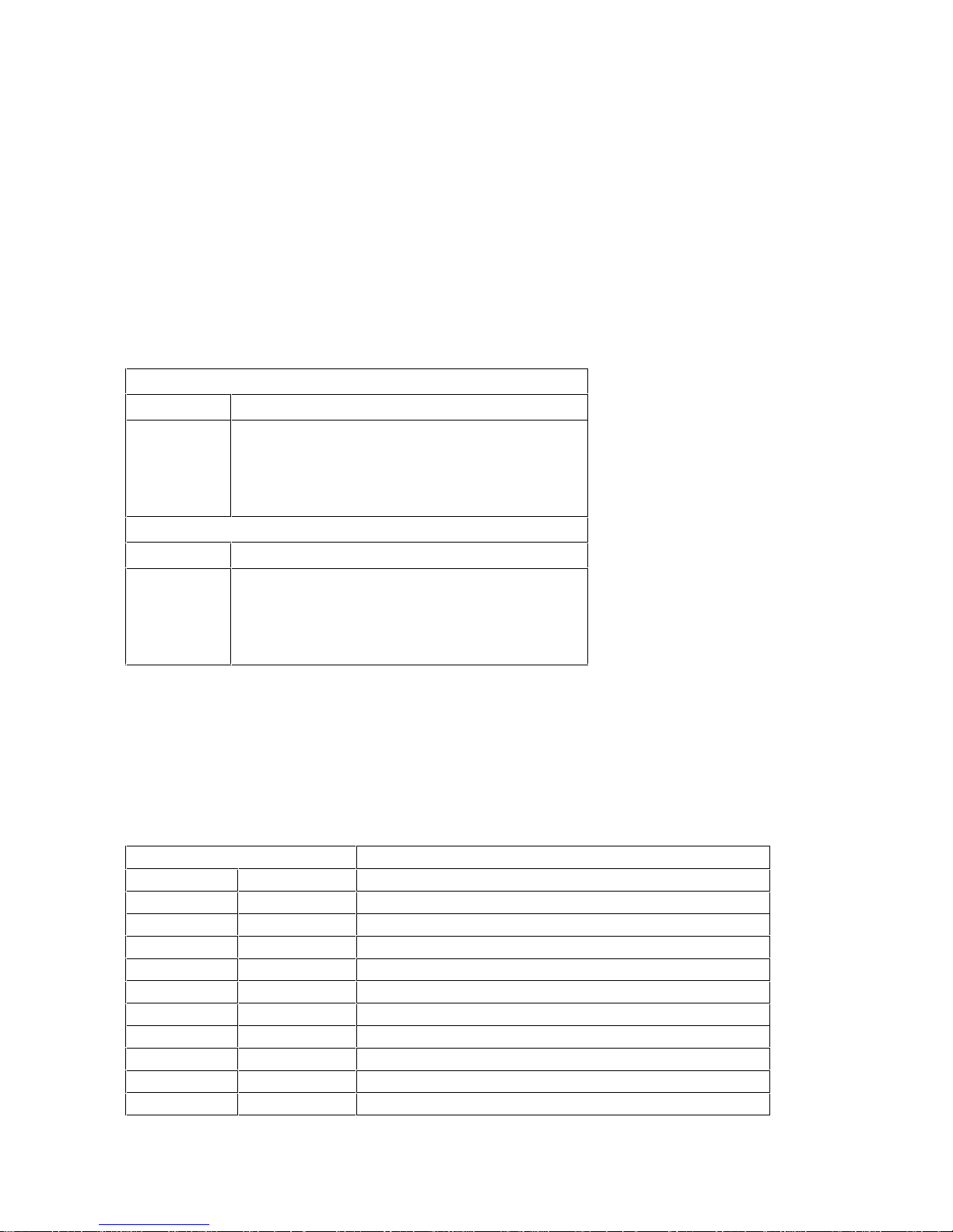
ADDRESSING SYSTEM BOARD COMPONENTS
IRQ0(08h)
IRQ1(09h)
IRQ2(0Ah)
This section provides more details of how the BIOS uses the system board components mentioned
in the I/O port list.
DMA Channel Controllers
Only “I/O-to-memory” and “memory-to-I/O” transfers are allowed.“I/O-to-I/O” and “memory-tomemory” transfers are disallowed by the hardware configuration.
The system controller supports seven DMA channels, each with a pageregister used to extend the
addressing range of the channel to 16 MB. The following table summarizes how the DMA channels
are allocated.
First DMA controller (used for 8-bit transfers)
Channel Function
0
1
2
3
Second DMA controller (used for 16-bit transfers)
Channel Function
4
5
6
7
Available
SoundBlaster or ECP mode for parallel port
Flexible disk I/O
ECP mode for parallel port or SoundBlaster
Cascade from first DMA controller
SoundBlaster or Available
Available or SoundBlaster
Available
Interrupt Controllers
The system has two 8259A compatible interrupt controllers. They are arranged as a master
interrupt controller and a slave that is cascaded through the master.
The following table shows how the master and slave controllers are connected. The Interrupt
Requests (IRQ) are numbered sequentially, starting with the master controller, and followed by the
slave.
IRQ (Interrupt Vector) Interrupt Request Description
System Timer
Keyboard Controller
Slave IRQ Cascade connection from INTC2 (Interrupt Controller 2)
IRQ8(70h) Real Time Clock
IRQ9(71h) Available for accessory board (ISA/PCI)
IRQ10(72h) SoundBlaster3, or Available for accessory board (ISA/PCI)
IRQ11(73h) Available for accessory board (ISA/PCI)
IRQ12(74h) Mouse, or ISA accessory board
IRQ13(75h) Co-processor
IRQ14(76h) IDE, or ISA accessory board
IRQ15(77h) 2nd IDE or ISA/PCI accessory board
Page 41

IRQ3(0Bh)
Serial Port 2, Serial Port 4, or ISA accessory board
IRQ4(0Ch)
IRQ5(0Dh)
IRQ6(0Eh)
IRQ7(0Fh)
Serial Port 1, Serial Port 3, or ISA accessory board
SoundBlaster1, Parallel Port 2, or ISA accessory board
Flexible Disk Controller
SoundBlaster2, Parallel Port 1, or ISA accessory board
Using the
Setup
program:
• IRQ3 can be made available by disabling serial ports 2 and 4.
• IRQ4 can be made available by disabling serial ports 1 and 3.
• IRQ5 can be made available by disabling the parallel port 2.
• IRQ7 can be made available by disabling parallel ports 1 and 2.
• IRQ12 can be made available by disabling the mouse interrupt.
PCI Interrupt Request Lines
PCI devices generate interrupt requests using up to four PCI interrupt request lines (INTA#,
INTB#, INTC#, and INTD#).
When a PCI device makes an interrupt request, the request is re-directed to the system interrupt
controller. The interrupt request will be re-directed to one of the IRQ lines made available for PCI
devices.
All PCI devices with interrupt transfer support will use and share INTA#.A PCI device supporting
multiple functionalities may use several INT lines. These devices will require more than one
system interrupt request line.
Page 42
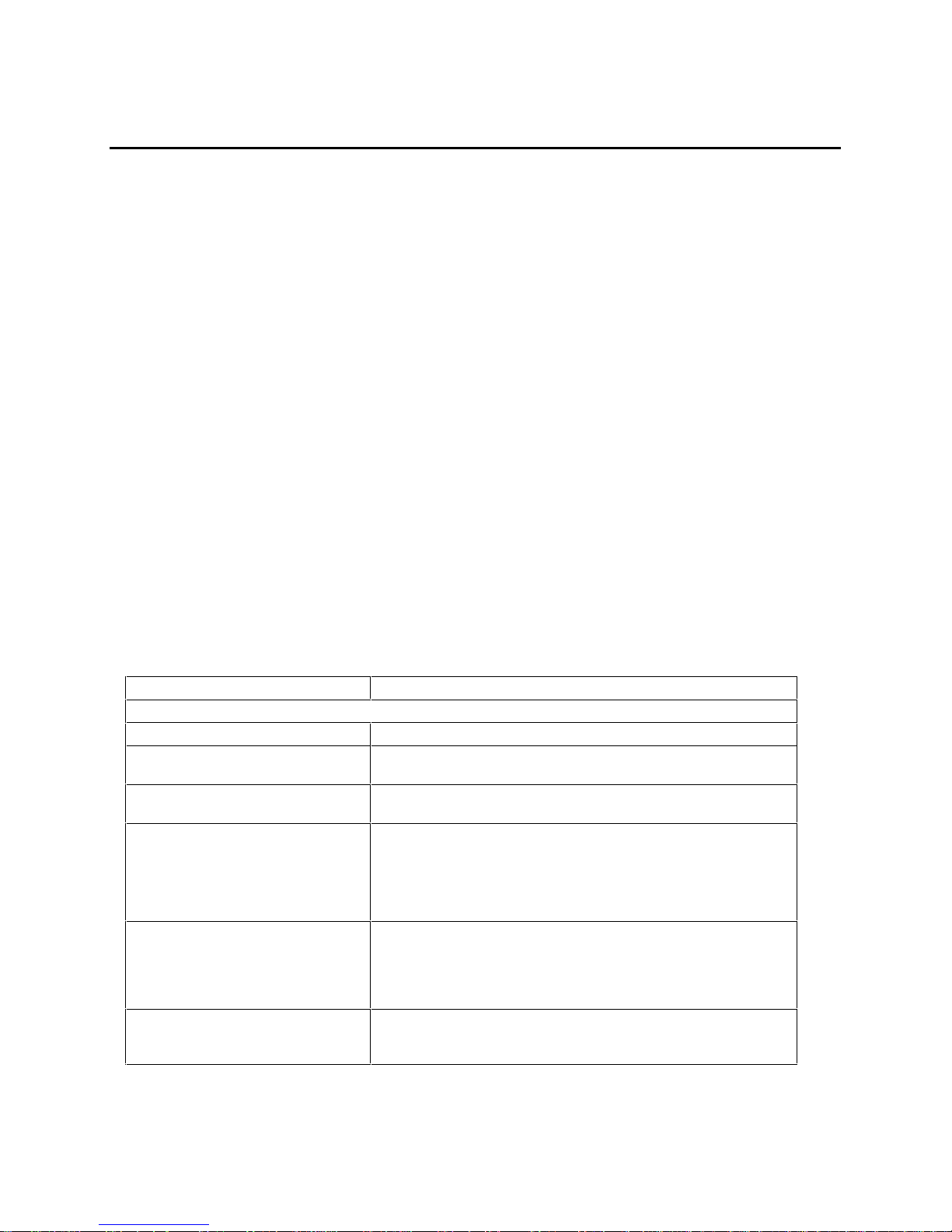
5 POWER-ON SELF-TEST ROUTINES
This chapter summarizes the Power-On Self-Test (POST) routines. The first section indicates the
order in which the tests are conducted. The second section lists the error codes which can be
reported, along with theirmeanings. The third section summarizes the suggested corrective action
appropriate for each error code.
VIEWED ON THE SCREEN
Each time the PC is turned on, or a reset is performed, the Power-On Self-Test (POST, also
referred to as the
HP System Hardware Test
functionality of the system components and initializes certain system parameters. It starts by
displaying the initial “Vectra” screen. Although the POST routines are run as normal, their progress
is not displayed (other than on the eight-stage graphics histogram underneath the “Vectra” label). If
POST detects an error, the results are reported on a
) is executed. The POST process verifies the basic
View System Errors
screen.
During the POST, the BIOS and other ROM data is copied into high-speed
shadow RAM
, where it
is addressed at the same physical location as the original ROM in a manner which is completely
transparent to applications. This technique provides faster access to the system BIOS firmware.
If the POST is initiated by a soft reset [CTRL] [ALT] and [DELETE], the RAM tests are not
executed and shadow RAM is not cleared. In all other respects, the POST executes in the same
way following power-on or a soft reset.
The POST detects when a hard disk has been replaced, or if there have been changes in the size
of the hard disk. However, it does not report an error.
The POST performs the tests in the order described here:
POST Test Description
System BIOS Tests
LED Test
System (BIOS) ROM Test
RAM Refresh Timer Test
Interrupt RAM Test
Shadow the System ROM BIOS
Load CMOS Memory
Tests the LEDs on the control panel.
Calculates an 8-bit check-sum. Test failure causes the boot
process to abort.
Tests the RAM refresh timer circuitry. Test failure causes the
boot process to abort.
1 Tests for RAM parity errors.
2 Checks the first 64 KB of system RAM used to store data
corresponding to various system interrupt vector
addresses.
Test failures cause the boot process to abort.
Tests the system ROM BIOS and shadows it. Failure to
shadow the ROM BIOS will cause an error code to display. The
boot process will continue, but the system will execute from
ROM. This tests is not performed after a soft reset (using
[CTRL] [ALT] and [DELETE])
Checks the serial EEPROM and returns an error code if it has
been corrupted. Copies the contents of the EEPROM into
CMOS RAM.
Page 43
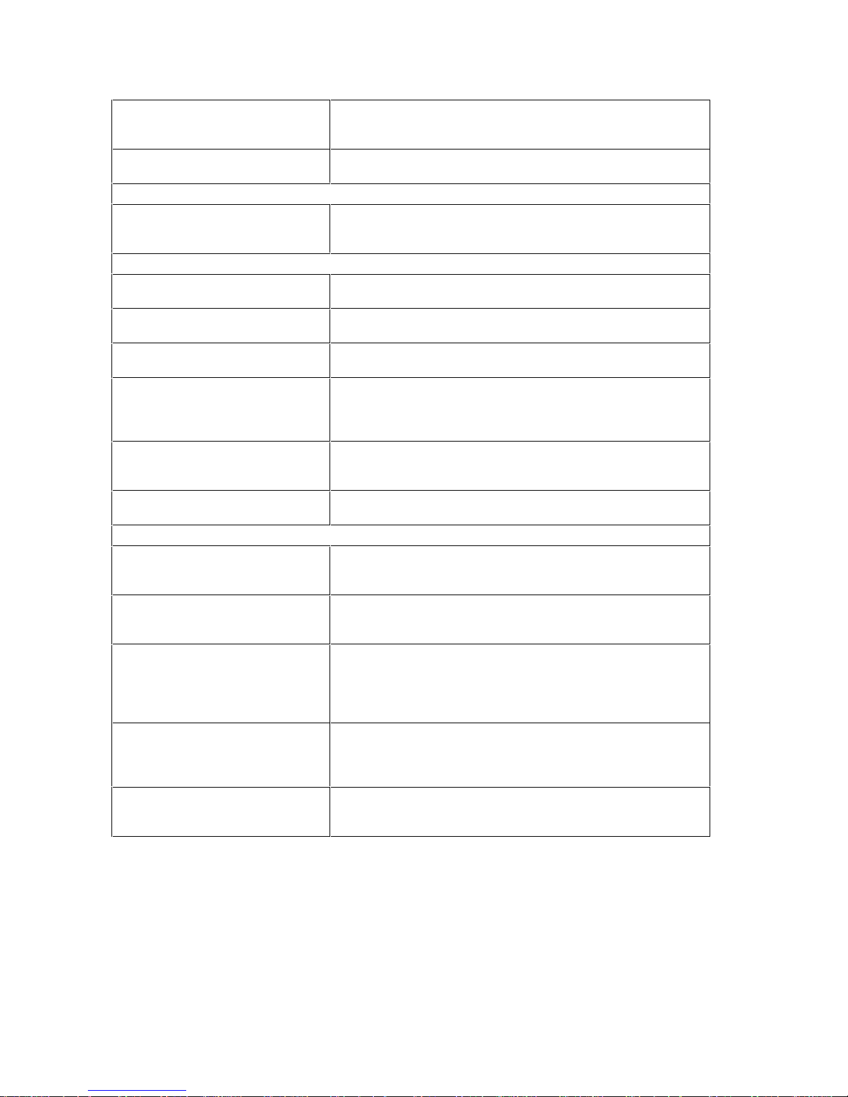
CMOS RAM Test
CPU Cache Memory Test
Initialize the Video
8042 Self-Test
Timer 0/Timer 2 Test
DMA Subsystem Test
Interrupt Controller Test
Real-Time Clock Test
Audio Test
RAM Address Line
Independence Test
Size Extended Memory
Real-Mode Memory Test
(First 640KB)
Shadow RAM Test
Protected Mode RAM Test
(Extended RAM)
Checks the CMOS RAM for start-up power loss, verifies the
CMOS RAM checksum(s). Test failure causes error codes to
display.
Tests the processor’s cache memories. Test failure causes an
error code to be displayed and the boot process to abort.
Video Tests
Initializes the video subsystem, tests the video shadow RAM,
and, if required, shadows the video BIOS. A failure causes an
error code to display, but the boot process continues.
System Board Tests
Downloads the 8042 and invokes the 8042 internal self-test. A
failure causes an error code to display.
Tests Timer 0 and Timer 2. Test failure causes an error code to
display.
Checks the DMA controller registers. Test failure causes an
error code to display.
Tests the Interrupt masks, the master controller interrupt path
(by forcing an IRQ0), and the industry-standard slave controller
(by forcing an IRQ8). Test failure causes an error code to
display.
Checks the real-time clock registers and performs a test that
ensures that the clock is running. Test failure causes an error
code to display.
Tests that a SoundBlaster chip is present, and invokes a builtin self-test. Test failure causes an error code to display.
Memory Tests
Verifies the address independence of real-mode RAM (no
address lines stuck together). Test failure causes an error code
to display.
Sizes and clears the protected mode (extended) memory and
writes the value into CMOS bytes 30h and 31h. If the system
fails to switch to protected mode, an error code is displayed.
not
Read/write test on real-mode RAM. (This test is
done
during a reset using [CTRL] [ALT] and [DELETE]). The test
checks each block of system RAM to determine how much is
present. Test failure of a 64 KB block of memory causes an
error code to display, and the test is aborted.
Tests shadow RAM in 64 KB segments (except for segments
beginning at A000h, B000h, and F000h). If they are
not
being
used, segments C000h, D000h and E000h are tested. Test
failure causes an error code to display.
Tests protected RAM in 64 KB segments (above 1 MB). (This
not
test is
done during a reset using [CTRL] [ALT] and
[DELETE]). Test failure causes an error code to display.
Page 44
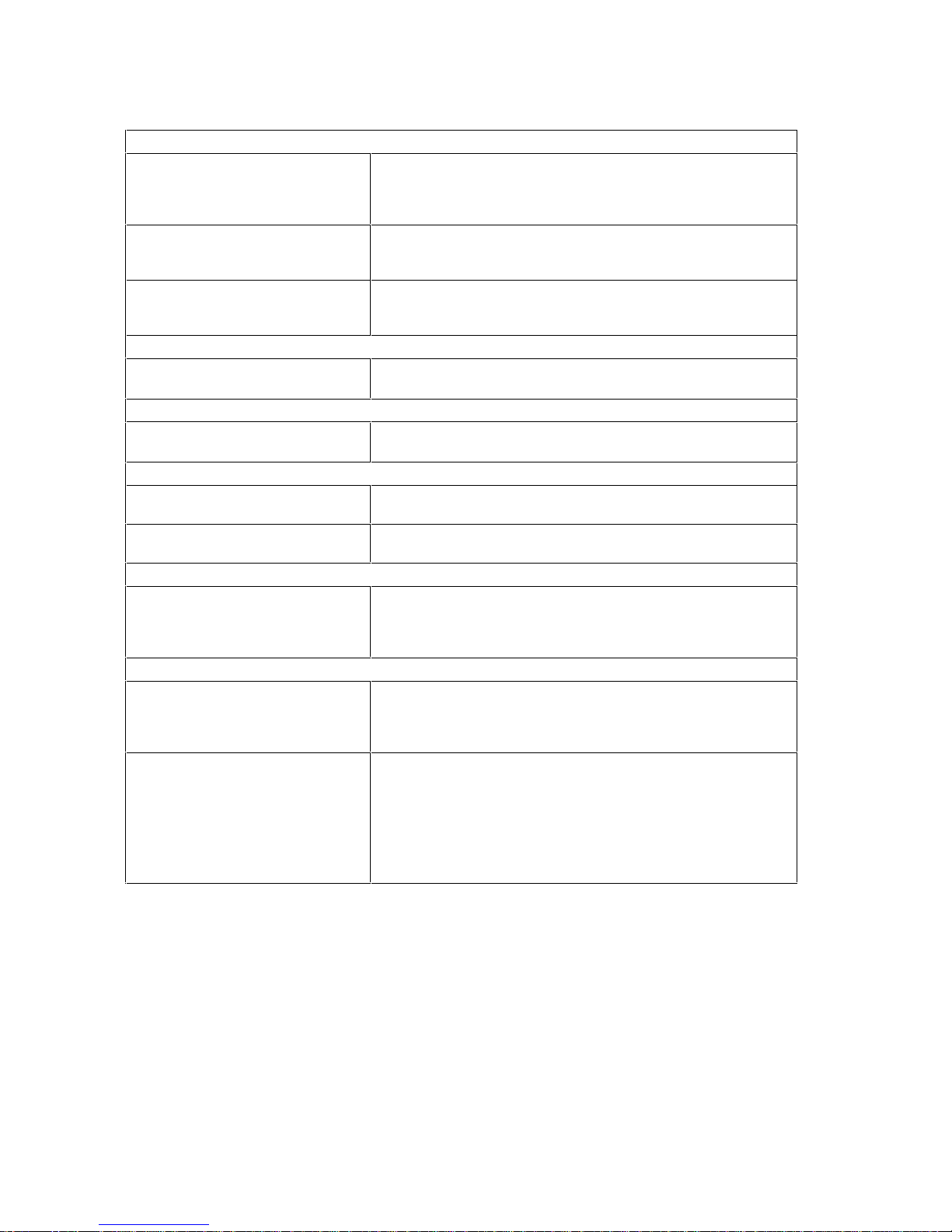
Keyboard Test
Mouse Test
LAN Test
Flexible Disk Controller
Subsystem Test
Internal Numeric Coprocessor
Test
Parallel Port Test
Serial Port Test
Hard Disk Controller
Subsystem Test
System Generation
Plug and PlayConfiguration
Keyboard / Mouse Tests
Invokes a built-in keyboard self-test of the keyboard’s
microprocessor and tests for the presence of a keyboard and
for stuck keyboard keys. Test failure causes an error code to
display.
If a mouse is present, invokes a built-in mouse self-test of the
mouse’s microprocessor and for stuck mouse buttons. Test
failure causes an error code to display.
If the HP PCI Integrated 10/100 VG Interface is present,
invokes a built-in self-test. Test failure causes an error code to
display.
Tests of Flexible Disk Drive A
Tests for proper operation of the flexible disk controller. Test
failure causes an error code to display.
Coprocessor Tests
Checks for proper operation of the numeric coprocessor part of
the processor. Test failure causes an error code to display.
Communication Port Tests
Tests the integrated parallel port registers, as well as any other
parallel ports. Test failure causes an error code to display.
Tests the integrated serial port registers, as well as any other
serial ports. Test failure causes an error code to display.
Hard Disk Drive Tests
Tests for proper operation of the hard disk controller. Test
failure causes an error code to display. The test does not
detect hard disk replacement or changes in the size of the hard
disk.
System Configuration Tests
Initiation of the system generation (SYSGEN) process, which
compares the configuration information stored in the CMOS
memory with the actual system. If a discrepancy is found, an
error code will be displayed.
Configures any Plug and Play device detected (either PCI or
ISA):
• All PCI devices, and any ISA device necessary for loading
the operating system will be configured for use.
• Any ISA device that is not required for loading the operating
system, will be initialized (prepared for loading of a device
driver), but not fully configured for use.
ERROR CODES
POST error codes are returned and, if possible, displayed when an error is detected during the
execution of the power-on self-test procedures. As well as the four digit code number, the error
message utility automatically displays an error diagnosis and suggestions for corrective action.
An exhaustive list of the error codes is given here, and a list of the suggested corrective actions is
given in the next section. In order to use these lists, you need to find the appropriate four digit,
hexadecimal, error code in the list below. These have been sorted into numerical order, to make it
easy to find the appropriate entry. (In this, two dots are used to represent a range of values, such
Page 45

as “4..7”, which means “4 or 5 or 6 or 7”, and the letter “x” is used to mean “any hexadecimal digit,
0..F”).
Underneath each error code, there is a short summary of the error diagnosis.
In order to find the suggested corrective action (SCA), it is necessary to read the five-character
code that is given on the right of the error code. This SCA code can then be found in the list that is
given in the next section of this chapter.
Not all of these error codes can be generated by the
6/xxx PC
. However, the complete list is given here, to allow for possible future changes to the
HP Vectra XU 6/xxx PC
or
HP Vectra VT
models within this product line.
0000 An error of unspecified origin (no other error code was
appropriate).
000E A thermal error occurred during your last session. SCA33
0080..00DF The ROM on an accessory board or the system board is
corrupted.
0110..011F, 0120 The real-time clock has failed. SCA01
0130 The system date and time has not been entered or has been lost
or corrupted.
0240 The system configuration has been lost. SCA04
0241, 0280 The system configuration has been lost or corrupted. SCA04
0250
02C0, 02C1 The master configuration information (stored in EEPROM) has
02C2 The Plug and Play Configuration Information has been corrupted.
02D0 The PC Serial Number is not set. SCA27
0300..031F The keyboard/mouse controller on the system board has failed. SCA06
0342, 0352, 0354 The keyboard or its cable has failed. SCA07
0343..0346, 0350,
0351, 0353, 0360
03E0..03E4, 03EC The mouse or the mouse controller on the system board has
03E5..03EB The mouse has failed. SCA08
0401 The system board has failed to switch to protected mode. SCA01
0505 The system board's serial port has failed. SCA09
0506 The built-in serial port's address is used by a serial port on an
0507 The system board's serial port at address 3F8h has failed. SCA09
0508 The system board's serial port at address 2F8h has failed. SCA09
0509 The system board's serial port at address 3E8h has failed. SCA09
050A The system board's serial port at address 2E8h has failed. SCA09
0510 The infra red port has failed. SCA26
0545 The system board's parallel port has failed. SCA09
0546 The built-in parallel port's address is used by a parallel port on an
The
Setup
information does not match the hardware installed in
the computer.
been lost or corrupted
Your adapters may not function correctly.
The keyboard or the keyboard controller on the system board has
failed.
failed.
accessory board.
accessory board.
SCA24
SCA02
SCA03
SCA05
SCA04
SCA30
SCA06
SCA06
SCA10
SCA10
Page 46

05F0 The built-in I/O controller's address is used by an accessory
SCA34
board. The following devices may not function properly:
keyboard, mouse, serial and parallel ports, flexible disk drives,
configuration information (serial EEPROM and CMOS RAM),
real-time-clock, and configuration switches.
0600..06FE One of the keys on the keyboard is stuck or a key was pressed
SCA11
during the power-on self-test.
06FF The mouse is connected to the keyboard port. SCA08
0700 The audio system cannot be initialized. SCA04
0800 The ROM on an accessory board uses the same address (E000h)
SCA12
as the system board's boot ROM.
0801
The boot ROM is enabled in
Setup
but a boot ROM is not present
SCA13
in the computer.
0811 The Integrated Ethernet Interface cannot be found at the I/O base
address specified in
Setup
.
SCA05
0812 The MAC address of the Integrated LAN Interface is corrupted. SCA01
0813 The Integrated Ethernet Interface registers cannot be initialized. SCA01
0814 The Integrated Ethernet Interface DMA transfer cannot be
SCA01
initialized.
0815 The Integrated Ethernet Interface internal registers read and write
SCA05
test failed.
0816 The Integrated Ethernet Interface configuration information is
SCA04
corrupted.
0817 The EEPROM containing the configuration parameters of the
SCA32
LAN Interface is corrupted.
081A The Integrated Ethernet Interface internal loopback test failed. SCA01
0900 The microprocessor fan is not connected.
SCA23
*** WARNING *** This could result in damage to the
microprocessor!
0910 The speaker is not connected. SCA31
1100..110F,
The system board's timer has failed. SCA01
1200..120F
20xA Two different sized memory modules are in the same bank. SCA35
201B, 202B, 204B,
A memory error occurred during your last session. SCA37
208B
201C, 202C, 204C,
Several memory errors occurred during your last session. SCA38
208C
2110..212F,
The system board's DMA controller has failed. SCA01
2210..221F
4F00..4F0F A memory module has failed. SCA36A
6100..61FF, 6500,
A memory module or the system board has failed. SCA14
8x06
62F1 The system board's memory controller has failed. SCA01
6510, 6520 A memory module or the system board ROM has failed. SCA25
65C0..65DF Accessory board ROM(s) failed to be shadowed (copied) to RAM. SCA16
6600..66FF
Setup
information specifies a SCSI accessory board which is not
SCA16
detected inside the computer.
6700 The parameters returned by the display do not match the DDC1
SCA29
standard used by your PC for automatic set up of ergonomic
refresh rates.
7000..7FFF The system board's interrupt controller has failed. SCA01
Page 47

8x03, 8x04
8050 The built-in hard disk controller's address is used by a hard disk
8060 The system has detected that one or several IDE hard disks were
8400 The hard disk drive's boot sector has been corrupted. SCA20
9000..900F Flexible disk drive A, its cable, or the controller has failed. SCA17
9010 The built-in flexible disk controller's address is used by a flexible
9100..910F The second flexible disk drive, its cable, or the controller has
9200..910F The third flexible disk drive, its cable, or the controller has failed. SCA17
A001
A002, A00C The co-processor has failed. SCA22
B300 The memory cache has failed. SCA01
B320 The memory cache module has failed. SCA28
E000..EFFF. The RAM on an accessory board has failed. SCA15
Setup
's custom-configured hard disk drive information is
incorrect.
controller on an accessory board.
added or removed since the PC was previously started (booted).
disk controller on an accessory board.
failed.
Setup
's co-processor information does not match the hardware
installed in the computer.
SCA05
SCA19
SCA18
SCA19
SCA17
SCA05
SUGGESTIONS FOR CORRECTIVE ACTION
An exhaustive list of the suggestions for corrective action (SCA) is given here, to accompany the
list of the error codes that is given in the previous section. In order to find the suggested corrective
action, it is necessary to read the five-character code that is given on the right of the error code in
the previous section. This SCA code can then be found in the list in this section. These have been
sorted into numerical order, to make it easy to find the appropriate entry.
SCA01
• Your system board may need to be replaced. Contact your service representative.
SCA02
1 Remove or disable the ROM(s) on the accessory board one by one to determine which
one, if any, has failed.
2 If this fails to correct the problem, your system board may need to be replaced. Contact
your service representative.
SCA03
• For models without a battery, this problem may occur if the PC is left unplugged for
periods of 24 hours or more.
• For models with battery, replace the battery.
Setup
1 Run
2 If after running
to correct the date and time information.
Setup
the problem re-occurs even after a RESET or [CTRL] [ALT]
[DELETE], ensure that the CONFG switch on the system board is set to Off.
3 If all the above fail, your system board may need to be replaced. Contact your
service representative.
SCA04
Setup
1 Run
2 If after running
to correct the configuration information.
Setup
the problem re-occurs even after a RESET or [CTRL] [ALT]
[DELETE], ensure that the CONFG switch on the system board is set to Off.
3 If all the above fail, your system board may need to be replaced. Contact your service
representative.
Page 48

SCA05
Setup
1 Run
to view your configuration and correct any obvious errors.
2 If this fails to correct the problem, ensure that your hardware (accessory boards, disk
drives, switches, and jumpers) is configured correctly (refer to their manuals). In
particular, check that the CONFG switch on the system board is set to Off. Make a written
note of the configuration before closing the cover.
Setup
3 If hardware settings were changed, run
to update the configuration information.
SCA06
1 If possible, test the keyboard and mouse by connecting them to a working Vectra 286,
386, or 486 computer:
2 If the working computer fails, the keyboard or mouse is defective.
3 If the error remains on this computer, or if you cannot test the keyboard and mouse, you
may need to contact your service representative to determine if your system board needs
replacement.
SCA07
1 Ensure the keyboard is firmly connected to the correct connector on the rear of the
computer.
2 If the problem persists, your keyboard may need to be replaced. Contact your service
representative.
SCA08
1 Ensure the mouse is firmly connected to the correct connector on the rear of the
computer.
2 If the problem persists, your mouse may need to be replaced. Contact your service
representative.
SCA09
• Your system board may need to be replaced. Contact your service representative.
Setup
• As a temporary solution, if you do not need the defective port, run
to disable it.
SCA10
• Either re-configure your accessory board or run
Setup
to re-configure your built-in port.
SCA11
1 Re-start your computer. Do not press a key during the power-on tests.
2 If the problem persists, check visually if a key is stuck on the keyboard and try to loosen it
gently.
3 If this fails to correct the problem, your keyboard may need to be replaced. Contact your
service representative.
SCA12
Setup
• Either re-configure or remove the accessory board ROM, or run
to disable the
system board's boot ROM.
SCA13
Setup
HP6Init
to disable it.
to re-initialize it (refer to the manual).
1 If you do not need the boot ROM, run
2 If you need to use the boot ROM, run
Page 49

SCA14
1 Ensure that all the memory modules are firmly seated in their sockets on the system
board.
2 If the problem persists, your system board may need to be replaced. Contact your service
representative.
SCA15
• Your accessory board or its memory may need to be replaced. Contact your service
representative.
SCA16
Setup
1 Run
to disable SCSI BIOS ROM shadowing.
2 If this fails to correct the problem, your system board may need to be replaced. Contact
your service representative.
SCA17
Setup
1 Run
to verify your configuration information. Correct it if necessary.
2 Ensure that all the disk cables are firmly connected.
3 If the problem persists, your disk drive or cable may need to be replaced. Contact your
service representative.
SCA18
Setup
1 Run
to configure IDE hard disk drives:
• if you have removed drive(s), confirm it by selecting the 'None or SCSI' field for the
corresponding drive.
• if you have added drive(s), confirm the new detected parameters by saving
configuration with [F3].
2 If the hard disk configuration has not been modified, it is likely one of the drives has no
longer been detected (in which case it was not identified on the POST screen).
3 Check cables are firmly plugged, and if the problem persists, contact your HP
representative.
SCA19
Setup
• Either disable the disk controller on the accessory board or run
to disable the built-
in disk controller.
SCA20
• Caution: this problem can be caused by a virus. See your reseller for anti-virus software.
1 If you wish to save the data located on your disk drive, you should use a
commercially available data recovery program.
2 If you do not wish to save the data, re-format the hard disk (refer to the operating
system manual).
SCA21
• Replace the microprocessor on the system board (refer to the manual).
SCA22
• Replace the co-processor on the system board (refer to the manual).
SCA23
• Please, turn off the unit until you have reconnected the microprocessor's fan to the
system board (refer to the manual).
• If the problem persists, your fan may need to be replaced. Contact your service
representative.
Page 50

SCA24
• Contact your service representative.
SCA25
1 Ensure that all the memory modules are firmly seated in their sockets on the system
board.
2 If this fails to correct the problem, run
HP6Init
to re- initialize the system board's ROM
(refer to the manual).
3 If the problem persists, your system board may need to be replaced. Contact your service
representative.
SCA26
• Your infrared interface may need to be replaced. Contact your service representative. As
a temporary solution, if you do not need the defective infra red port, run
Setup
it.
SCA27
Setup
1 Run
to enter the serial number of your system. You will find the Serial Number
printed on the rear of the computer.
2 If this fails to correct the problem, your system board may need to be replaced. contact
your service representative.
SCA28
1 Ensure that the memory cache module is firmly seated in its socket on the system board.
2 If this fails to correct the problem, your system board may need to be replaced. contact
your service representative.
to disable
SCA29
• Run Setup to set the "Display Plug and Play" parameter to "Disabled" to avoid a blank
screen at power on (or improper DMI recognition).
SCA30
Setup
1 Run
and the error will be corrected for you on [F3] exit.
2 If necessary, run your Plug and Play Configuration software to restore the information
that was lost.
3 If the problem persists, a component may be defective. Contact your service
representative.
4 You may also use the clear configuration switch, but you will have to re-initialize all your
Setup
configuration with
.
SCA31
• Please, turn off the unit until you have reconnected the speaker to the system board
(refer to the manual).
• If the problem persists, your speaker may need to be replaced. Contact your service
representative.
SCA32
• Your LAN Interface may need to be replaced. Contact your service representative.
SCA33
1 Check that the fan air flow is not obstructed.
2 Check that the fan is well connected.
Setup
3 Run
to clear the error.
Page 51

SCA34
• Re-configure your accessory board. Check your manual and
resources are used by the internal devices.
Machine-Dependent Actions:
SCA35
• Replace the memory modules as follows:
Error code Replace module in:
201A Slot A or Slot B
202A Slot C or Slot D
204A Slot E or Slot F
208A Slot G or Slot H
SCA36
• Replace the memory modules as follows:
Error code Replace module in:
4F01 Slot A
4F02 Slot B
4F03 Slot C
4F04 Slot D
4F05 Slot E
4F06 Slot F
4F07 Slot G
4F08 Slot H
Setup
to see which
SCA37
• The memory error that was detected during the last session has been corrected. Run
Setup
to clear the error.
• If this message appears in the future again with the same error code, you should replace
a memory module in that location:
Error code Replace module in:
201B Slot A1 or Slot A2
202B Slot B1 or Slot B2
204B Slot C1 or Slot C2
208B Slot D1 or Slot D2
SCA38
• One of the memory modules must be replaced.
The following table indicates the location:
Error code Replace module in:
201C Slot A1 or Slot A2
202C Slot B1 or Slot B2
204C Slot C1 or Slot C2
208C Slot D1 or Slot D2
Setup
• Run
to clear the error.
 Loading...