

Page 1

Technical Reference
Manual
Hardware and BIOS
HP Vectra VL 5/xx series 4 PC
and
HP Vectra VL 5/xx MT series 4 PC
December 1995
Page 2

NOTICE
Information contained in this document is subject to change without notice.
Hewlett-Packard makes no warranty of any kind with regard to this material, including,
but not limited to, the implied warranties of merchantability and fitness for a particular
purpose. Hewlett-Packard shall not be liable for errors contained herein or for incidental
or consequential damages in connection with the furnishing, performance, or use of
this material.
Hewlett-Packard shall not be liable for errors contained herein or for incidental or consequential
damages in connection with the furnishing, performance, or use of this material.
Hewlett-Packard assumes no responsibility for the use or reliability of its software on equipment
that is not furnished by Hewlett-Packard.
This document contains proprietary information which is protected by copyright. All rights are
reserved. No part of this document may be photocopied, reproduced, or translated into another
language without the prior written consent of Hewlett-Packard Company.
Centronics® is a U.S. registered trademark of Centronics Data Computer Corporation.
LANManager, Microsoft Windows, Windows 95 and OS/2 are products of Microsoft
Corporation.
Microsoft® and MS-DOS® are registered trademarks of Microsoft Corporation.
Novell® and Netware® are registered trademarks of Novell Inc.
Pentium™ is a trademark of Intel Corporation.
©1995 Hewlett-Packard Company
Page 3

Table of Contents
NOTICE 2
PREFACE 5
ORDERING INFORMATION FOR THE PHOENIX BIOS MANUAL 5
CONVENTIONS 5
BIBLIOGRAPHY 6
1 SYSTEM OVERVIEW 7
SYSTEM OVERVIEW 7
HP VECTRA VL 5/XX SERIES 3 – VL 5/XX SERIES 4 COMPARISON 7
HP VECTRA VL 5/XX SERIES 4 DESKTOP – MINI-TOWER
COMPARISON 8
VL 5/XX SERIES 4 PC BLOCK DIAGRAM 9
PRINCIPAL COMPONENTS AND FEATURES 9
VL 5/XX SERIES 4 SYSTEM BOARD 10
VL 5/XX MT SERIES 4 DESKTOP BACKPLANE 11
VL 5/XX MT SERIES 4 MINI-TOWER BACKPLANE 11
PROCESSOR 11
SUPERSCALAR ARCHITECTURE 12
FLOATING POINT UNIT (FPU) 12
DYNAMIC BRANCH PREDICTION 12
INSTRUCTION AND DATA CACHE 12
DATA INTEGRITY 13
PCI CHIP SET 13
PCI, CACHE AND MEMORY CONTROLLER (82437FX) 14
DATA PATH UNIT (82438FX) 15
THE PCI/ISA BRIDGE AND IDE CONTROLLER (82371FB) 15
THE 82438FX AND 82371FB FEATURE SUMMARY 16
SUPER I/O CHIP 1 7
NS PC87332VF FEATURE SUMMARY 17
FLEXIBLE DRIVE CONTROLLER (FDC) 17
SERIAL/PARALLEL PORTS 18
GRAPHICS/INTEGRATED VIDEO 18
IDE TO PCI CONTROLLER 19
FLASH ROM 19
SECURITY FEATURES 19
PHYSICAL CHARACTERISTICS 19
ELECTRICAL SPECIFICATIONS 20
POWER AVAILABILITY (CONTINUOUS OPERATION): 20
ENVIRONMENTAL SPECIFICATIONS 21
2 SUMMARY OF THE HP/PHOENIX BIOS 22
HP/PHOENIX BIOS DESCRIPTION 22
OVERVIEW OF ADDRESS SPACE 22
I/O ADDRESSES USED BY THE SYSTEM* 22
BIOS I/O PORT MAP 23
Page 4

ADDRESSING SYSTEM BOARD COMPONENTS 24
3 DESKTOP MANAGEMENT INTERFACE 26
DMI INFORMATION STRUCTURE 26
ACCESSING BIOS DMI INFORMATION 27
THE DMI HEADER 28
VERIFYING THE DMI INFORMATION STRUCTURE 28
DMI SUB-STRUCTURE TABLES 2 9
4 POWER-ON SELF-TESTS AND ERROR MESSAGES 32
POWER-ON SELF TEST (POST) 32
SHADOW RAM 32
ERROR MESSAGES 34
BEEP CODES 36
5 THE ULTRA VGA VIDEO CONTROLLERS 37
THE MATROX MGA MILLENNIUM VIDEO ADAPTER BOARD 37
VIDEO MEMORY 37
AVAILABLE VIDEO RESOLUTIONS 37
VESA CONNECTOR 38
FURTHER INFORMATION 38
THE INTEGRATED ULTRA VGA VIDEO CONTROLLER 38
VIDEO MEMORY 39
VIDEO MODES 39
AVAILABLE BIOS VIDEO RESOLUTIONS 42
VESA CONNECTOR 43
DB15 CONNECTOR PINOUT 43
VIDEO CONTROLLER SUMMARY 43
Page 5

PREFACE
This manual is a technical reference and BIOS document for engineers and technicians
providing system level support. It is assumed that the reader possesses a detailed
understanding of AT-compatible microprocessor functions and digital addressing techniques.
Technical information that is readily available from other sources, such as manufacturer’s
proprietary publications, has not been reproduced.
This manual contains summary information only. For additional reference material, refer to the
bibliography.
ORDERING INFORMATION FOR THE PHOENIX BIOS MANUAL
System BIOS for IBM PCs, Compatibles, and EISA Computers
Phoenix Technologies is available in many bookstores. It can also be ordered directly from the
publisher as follows:
In the U.S.A.
Call Addison-Wesley in Massachusetts at +1-800-447-2226, and be prepared to give a credit
card number and expiry date.
In Europe
Send your request to Addison-Wesley at the address given below, and be prepared to give a
credit card number and expiry date.
Addison-Wesley
Concertgebouwplein 25
1071 LM Amsterdam, The Netherlands
Tel: +31 (20) 671 72 96
Fax: +31 (20) 675 21 41
(ISBN 0-201-57760-7) by
CONVENTIONS
The following conventions are used throughout this manual to identify specific elements:
• Hexadecimal numbers are identified by a lower case h.
For example, 0FFFFFFFh or 32F5h
• Binary numbers and bit patterns are identified by a lower case b.
For example, 1101b or 10011011b
Page 6

BIBLIOGRAPHY
•
System BIOS for IBM PCs, Compatibles, and EISA Computers
Phoenix Technologies. Addison-Wesley (publisher).
The following Hewlett-Packard publications may also assist the reader of this manual.
(ISBN 0-201-57760-7) by
• HP Vectra VL 5/xx series 4 PC
• HP Vectra VL 5/xx MT series 4 PC
• HP Vectra VL 5/xx series 4 PC and HP Vectra VL 5/xx MT series 4 PC
(D3645-90901)
Guide
HP Vectra PC Service Handbook - 9th edition
•
The following Intel® publication provides more detailed information:
Pentium Processor
•
(241595-1)
User’s Guide
User’s Guide
(supplied with PC).
(supplied with PC).
(Available January 1996)
Familiarization
Page 7
1 SYSTEM OVERVIEW
This chapter provides a description of the HP Vectra VL 5/xx series 4 desktop and HP Vectra
VL 5/xx MT series 4 mini-tower PC with detailed system specifications.
SYSTEM OVERVIEW
The HP Vectra VL 5/xx series 4 PC is a Pentium processor, ISA/PCI-based PC and features
the Intel Triton chip set.
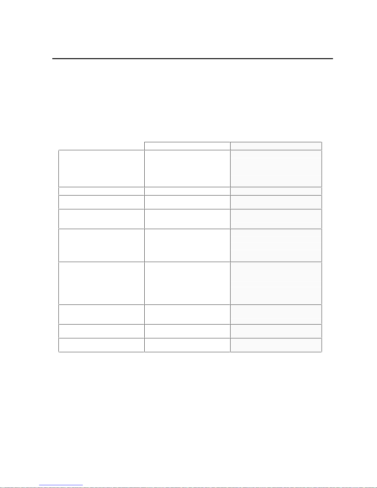
HP VECTRA VL 5/XX SERIES 3 – VL 5/XX SERIES 4 COMPARISON
Vectra VL 5/xx series 3 Vectra VL 5/xx series 4
Processor Pentium 75 (VL 5/75)
Pentium 90 (VL 5/90)
Pentium 100 (VL 5/100)
Pentium 120 (VL 5/120)
Level-two cache memory 256 KB asynchronous cache 256 KB synchronous cache
Main memory 8 MB or 16 MB standard
192 MB maximum
Video controller Cirrus Logic GD 5434
integrated on PCI bus
Video memory 1 MB standard
upgradable to 2 MB
Enhanced IDE hard disk controller CMD PCI0640B
Integrated on PCI bus
dedicated for hard disk drives
Secondary IDE controller Integrated in NS 87332 Super I/O
chip on ISA bus
dedicated for CD-ROM drives
Flexible disk controller Integrated in NS 87332 Super I/O
chip on ISA bus
Serial / parallel port controller Integrated in NS 87332 Super I/O
chip on ISA bus
Pentium 90
Pentium 100
Pentium 120
Pentium 133
Pentium 150
Pentium 166
8 MB or 16 MB standard
128 MB maximum
Trio 765 64V+ or 764 integrated on
PCI bus or
Matrox MGA Millennium video card
1 MB standard
upgradable to 2 MB
Matrox Models
2 MB standard
upgradable to 4 MB or 8 MB*
Integrated in chip set (part of
82371FB multipurpose chip)
Integrated on PCI bus
Primary channel dedicated for hard
disk drives
Secondary channel recommended for
CD-ROM drives
No secondary IDE controller
(Two channels on enhanced IDE
controller - see above)
Integrated in SMC 932 Super I/O chip
on ISA bus
Integrated in SMC 932 Super I/O chip
on ISA bus
*The 6 MB video upgrade module is available only from Matrox Electronic Systems Limited.
Page 8
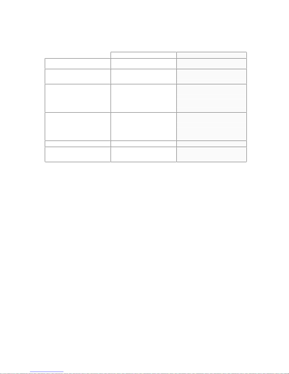
HP VECTRA VL 5/XX SERIES 4 DESKTOP – MINI-TOWER COMPARISON
Desktop Mini-Tower
IDE Controller
Primary channel connectors
IDE Controller
Secondary channel connectors
Flexible disk controller connectors Two connectors for 3.5-inch
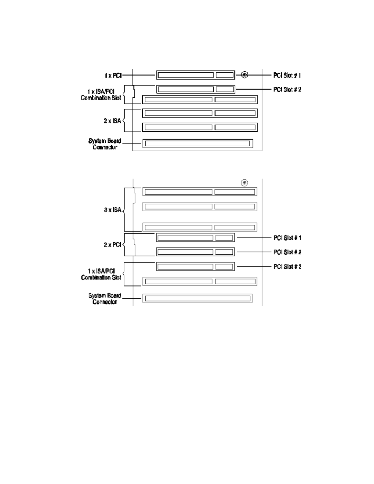
Accessory board slots (on
backplane)
Internal device shelves One for hard disk drive Two for hard disk drives
Front-access device shelves One 3.5-inch
Two connectors for hard disk
drives
One red connector recommended
for CD-ROM
flexible disk drive or tape drive
One 16-bit ISA (short 16cm/
6.3-inch)
One 16-bit ISA (full-length)
One 32-bit PCI/16-bit ISA
Combination (full-length)
One 32-bit PCI (full-length)
One 5.25-inch
One 5.25-inch, 1-inch high
Two connectors for hard disk drives
Two red connectors recommended for
CD-ROM and supplementary hard
disk drive
Two connectors for 3.5-inch flexible
disk drive or tape drive
One connector for 5.25-inch flexible
disk drive
Maximum two devices connected
simultaneously
Three 16-bit ISA (full-length)
One 32-bit PCI/16-bit ISA
Combination (short 16cm/ 6.3-inch)
Two 32-bit PCI (full-length)
One 3.5-inch
Three 5.25-inch
Page 9
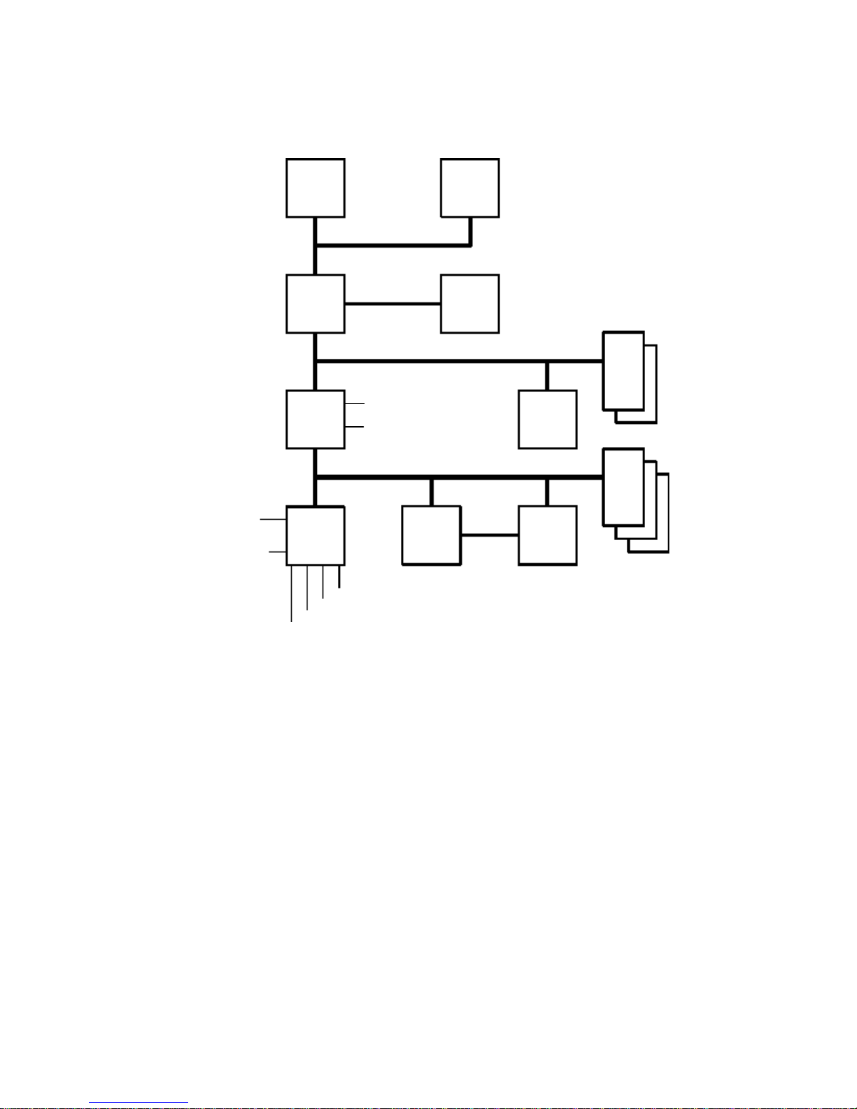
VL 5/XX SERIES 4 PC BLOCK DIAGRAM
ISA
Accessory
Board Slots
Keyboard
Mouse
Pentium
Processor
Intel Triton
82437/8FX
Chipset
Intel
82371FB
PCI/ISA
Bridge
SMC932
Super I/O
Controller
256 KB
Level-Two
Host Bus
Memory
(8 MB -
128 MB)
PCI Bus
IDE Controller Channel 1
IDE Controller Channel 2
ISA Bus
I/O
Decode
Logic
Cache
Flash
Support
PCI
Accessory
Board Slots
S3 Trio
Video
Controller
BIOS
Flash
ROM
FDD
Parallel
Serial 2
Serial 1
PRINCIPAL COMPONENTS AND FEATURES
The main features of the system board are:
• supports Pentium processors of several different clock speeds (90, 100, 120 or 133 MHz,
and 150 and 166 MHz when available) with accompanying voltage regulator module
(VRM)
• a PCI bus video controller: most models of the Vectra VL 5/xx series 4 have an integrated
64-bit Ultra VGA controller on the PCI bus (S3 Trio 765 64V+ on D3xxxA models and S3
Trio 764 on D3xxxB models)
• an Enhanced IDE controller with two channels on the PCI bus
• a primary IDE channel for two IDE hard disk drives
• a secondary IDE channel for an IDE CD-ROM drive and, in the mini-tower models, a
fourth IDE device (such as a third IDE hard disk drive)
Page 10
• a combined controller on the ISA bus for
• 2 flexible disk drives and/or tape drives
• 2 serial ports
• 1 parallel port
• sockets for DRAM main memory: the Vectra VL 5/xx series 4 PCs provide six sockets for
main memory, allowing installation of up to 128 MB
• a system ROM (using flash ROM technology) that can be easily updated with the latest
firmware, using the
Phlash.exe
program supplied with the firmware upgrade. The system
ROM contains:
• the BIOS (system BIOS, video BIOS and low option ROM)
• a power-on hardware test that allows you to view the results of the diagnostics as well
as a corrective action message (error message utility)
• menu-driven SETUP with context-sensitive help (in US English only)
• a keyboard/mouse controller and interface.
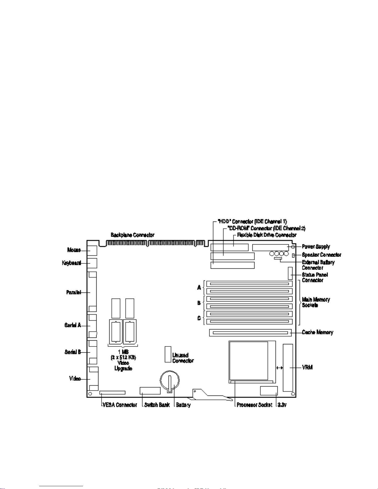
VL 5/XX SERIES 4 SYSTEM BOARD
*This video upgrade applieso nly to themodels with integrated video controller.
Page 11
VL 5/XX MT SERIES 4 DESKTOP BACKPLANE
VL 5/XX MT SERIES 4 MINI-TOWER BACKPLANE
PROCESSOR
The Pentium processor uses 64-bit architecture and is 100% compatible with Intel’s family of
x86 processors. All application software written for Intel386 and Intel486 processors can run on
the Pentium without modification. The Pentium processor contains all the features of the Intel
486 processor, with the following added features which enhance performance:
• Superscalar Architecture
• Floating Point Unit
• Dynamic Branch Prediction
• Instruction and Data cache
• Data Integrity
• Supports MultiProcessor Specification (MPS) 1.1
• PCI bus architecture
• Advanced Power Management capability for reducing power consumption
The processor is seated in a Zero Insertion Force (ZIF) socket.
Page 12

SUPERSCALAR ARCHITECTURE
The Pentium processor’s superscalar architecture has two instructions pipelines and a floatingpoint unit, each capable of independent operation. The two pipelines allow the Pentium to
execute two integer instructions in parallel, in a single clock cycle. Using the pipelines halves
the instruction execution time and almost doubles the performance of the processor, compared
with an Intel486 microprocessor of the same frequency.
Frequently, the microprocessor can issue two instructions at once (one instruction to each
pipeline). This is called instruction pairing. Each instruction must be simple. One pipeline will
always receive the next sequential instruction of the one issued to the other pipeline.
FLOATING POINT UNIT (FPU)
The Floating Point Unit incorporates optimized algorithms and dedicated hardware for multiply,
divide, and add functions. This increases the processing speed of common operations by a
factor of three.
DYNAMIC BRANCH PREDICTION
The Pentium processor uses dynamic branch prediction. To dynamically predict instruction
branches, the processor uses two prefetch buffers. One buffer is used to prefetch code in a
linear way, and one to prefetch code depending on the contents of the Branch Target Buffer
(BTB). The BTB is a small cache which keeps a record of the last instruction and address used.
It uses this information to predict the way that the instruction will branch the next time it is used.
When it has made a correct prediction, the branch is executed without delay, thereby
enhancing performance.
INSTRUCTION AND DATA CACHE
The Pentium processor has separate code and data caches on-chip. Each cache is 8 KB in size
with a 32-bit line. The cache acts as temporary storage for data and instructions from the main
memory. As the system is likely to use the same data several times, it is faster to get it from
the on-chip cache than from the main memory.
Each cache has a dedicated Translation Lookaside Buffer (TLB). The TLB is a cache of the
most recently accessed memory pages. The data cache is configured to be Write-Back on a
line-by-line basis (a line is an area of memory of a fixed size).
The data cache tags (directory entries used to reference cached memory pages) are triple
ported to support two data transfers and an inquire cycle in the same clock cycle. The code
cache tags are also triple ported to support snooping (a way of tracking accesses to main
memory by other devices) and split line accesses.
Individual pages of memory can be configured as cacheable or non-cacheable by software or
hardware. They can also be enabled and disabled by hardware or software.
Page 13
DATA INTEGRITY
PCI
Slave
The processor uses a number of techniques to maintain data integrity. It employs two methods
of error detection:
• Data Parity Checking
This is supported on a byte-by-byte basis, generating parity bits for data addresses sent
out of the microprocessor. These parity bits are not used by the external subsystems.
• Internally
The processor uses functional redundancy checking to provide maximum error detection
of the processor and its interface.
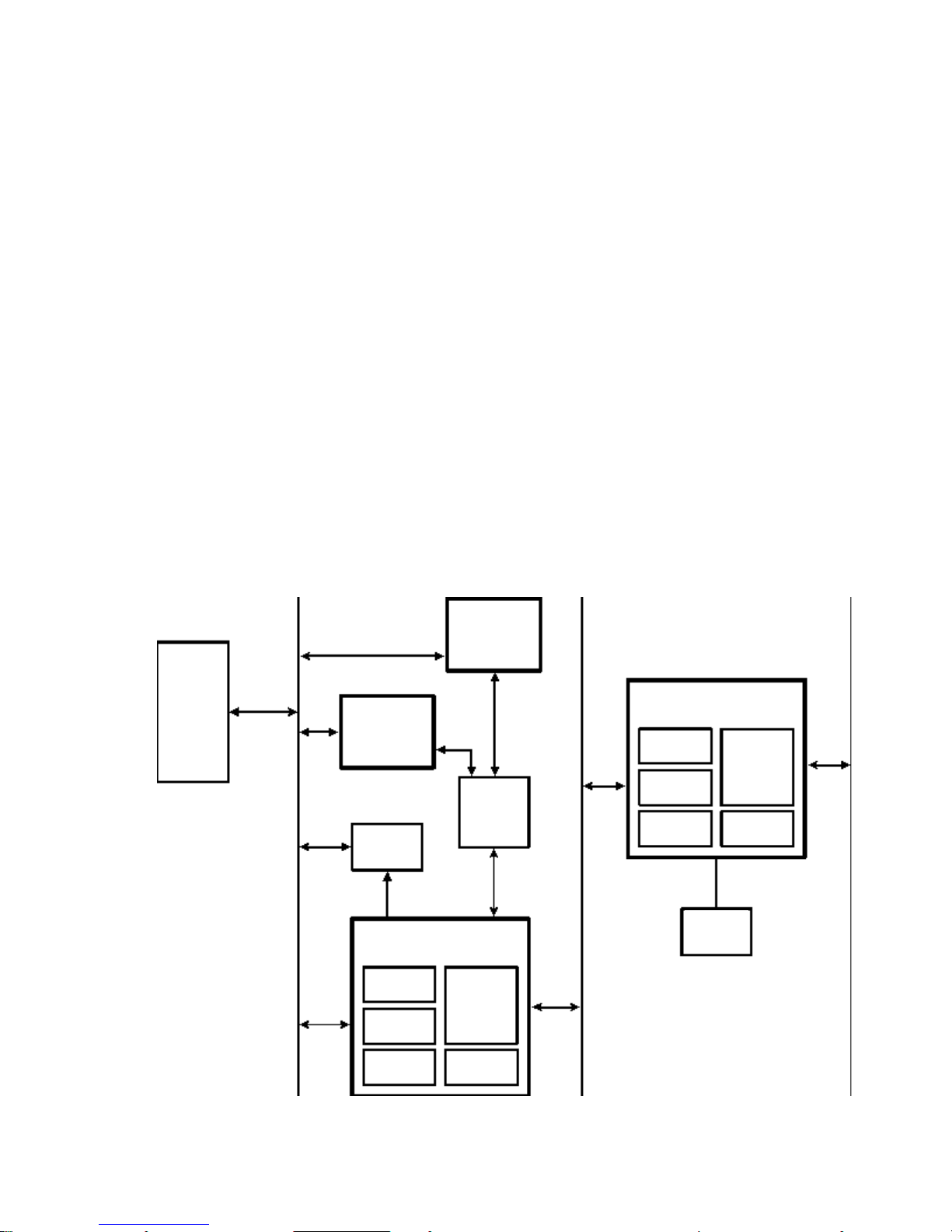
PCI CHIP SET
The chip set consists of three devices:
• The PCI, Cache, and Memory Controller (82437FX)
• Two Data Path Units (82438FX)
• The PCI/ISA bridge and IDE controller (82371FB)
The 82437FX and 82438FX2 devices provide the core cache and memory system architecture,
and the PCI interface.
Pentium
Processor
Host Bus
82438FX
Data Path Unit
Level-Two
Cache
82437FX PCI, Cache and
Memory Controller
Cache
Controller
Write
Buffer
82438FX
Data Path Unit
Main
Memory
Main
Memory
Controller
PCI Bus
82371Fb
PCI/ISA Bridge
PCI
Master
APIC
ISA Bus
ISA Bus
Controller
IDE
Controller
BIOS
PCI
Master
PCI
Slave
Page 14
PCI, CACHE AND MEMORY CONTROLLER (82437FX)
The 82437FX device integrates cache and memory control functions and provides bus control
functions for the transfer of information between the microprocessor, cache, main memory and
the PCI bus. The cache controller supports the Pentium Cache Write-Back mode and 256 KB
of direct mapped, write-back level-two cache, using synchronous pipeline burst SRAMs.
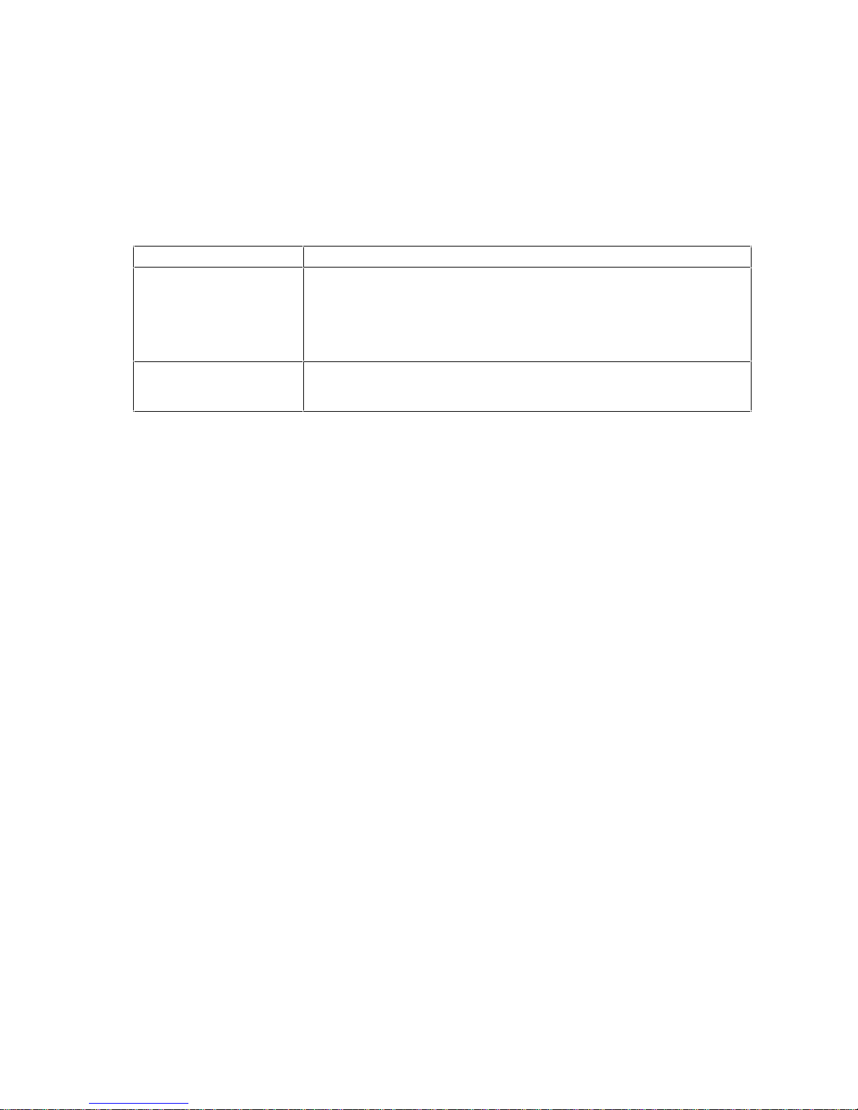
82437FX Feature Summary
Function Features
Cache controller • Direct mapped organization
• Buffered write-back
• External cache tags
• 32-byte line size
• Uses synchronous pipeline burst SRAM
• Supports 3-1-1-1* burst reads
Write buffer • Buffers all processor writes to main memory
• Buffers memory writes to PCI for selected memory regions
• Supports 3-1-1-1* write access timing
*The Pentium's internal cache has a 32-byte line size, which is four times the width of the Pentium's
host data bus. Burst reads and writes by the Pentium involve a full cache line, and so require four
back-to-back cycles to complete. The first cycle in each burst of four always requires more time to
complete than the three subsequent cycles. This is because the first cycle includes the addressing
phase and precharge timing (for memory).
Page 15

Function Features
DRAM controller • Uses dedicated DRAM memory address and data buses
• Page mode - one or two pages open simultaneously
• Supports pipelined accesses
• Full RAS/CAS programmability
• Flexible bank configurations (each bank programmable for DRAM
size, bank width and single or double-sided modules)
• Self configuring bank start addresses
• Shadow RAM support for the memory region 640 KB -
1 MB (in 16 KB segments)
• System management memory support
• RAS only refresh
• Fast memory access 7-2-2-2* with Extended Data Out (EDO) memory
PCI slave interface • Becomes processor (local) bus master to generate DRAM
requests on behalf of other PCI bus masters
• Supports PCI bus burst cycles
• Supports posted writes to DRAM for PCI burst writes
• Supports read-ahead from DRAM for PCI burst reads
PCI master interface • Provides for programmable PCI bus memory regions in
memory address map
• Supports PCI bus burst cycles for 64-bit and 32-bit misaligned Pentium
reads and writes
• Optional posting of PCI memory and I/O writes
• Optional buffering of PCI memory writes
• Optional read-ahead for processor to PCI accesses
PCI bus arbiter • Supports PCI bus arbitration for up to four masters
• Supports rotating priority scheme
*The Pentium's internal cache has a 32-byte line size, which is four times the width of the Pentium's
host data bus. Burst reads and writes by the Pentium involve a full cache line, and so require four
back-to-back cycles to complete. The first cycle in each burst of four always requires more time to
complete than the three subsequent cycles. This is because the first cycle includes the addressing
phase and precharge timing (for memory).
DATA PATH UNIT (82438FX)
The 82438FX component contains a 64-bit data path between the host bus and main memory.
A 4×64-bit deep buffer provides 3-1-1-1 writes to main memory.
This buffer is used for:
• writes from processor to main memory
• level-two cache write back cycles
• transfers from PCI to main memory.
THE PCI/ISA BRIDGE AND IDE CONTROLLER (82371FB)
The 82371FB device serves as a bridge between the PCI bus and the ISA expansion bus, and
incorporates a two-channel PCI IDE controller. It incorporates the logic for a PCI interface, a
DMA interface, a DMA controller that supports fast DMA transfers, data buffers to isolate the
PCI and ISA buses, Timer/Counter logic, and NMI control logic.
Page 16

The 82371FB PCI/ISA bridge also provides decode for the following peripheral devices:
• Flash BIOS
• Real Time Clock/CMOS Memory
• Keyboard/Mouse Controller
• Flexible Disk Controller
• Two Serial Ports
• One Parallel Port
• PCI Accessory Board Slots.
THE 82438FX AND 82371FB FEATURE SUMMARY
Function Features
Data buffer
(for 82438FX and 82371FB
together)
PCI master / slave interface
(for 82371FB only)
ISA bus controller
(for 82371FB only)
Fast IDE controller
(for 82371FB only)
• Provides a high performance 64-bit data path between
the processor (local) bus and main memory
• Provides a 32-bit data path to the PCI bus
• Provides a 8-deep x 64-bits wide write buffer for all
processor writes to main memory
• Provides a one-level posted write buffer for all processor writes
to PCI bus memory
• Fully compatible with PCI specification
• Supports PCI-to-ISA / ISA-to-PCI bus master cycle translations
• Supports programmable memory regions to provide fast positive
decode for PCI master accesses
• Implements subtractive decoding for unclaimed PCI cycles
• Supports PCI-to-ISA posted memory writes
• Translates DMA transfers for PCI slaves
• Supports PCI address/data parity generation and checking
• Fully compatible with ISA bus standard
• Supports asynchronous ISA bus operation up to 16 MHz
• Integrates:
• two 82C37A DMA controllers
• two 82C59A interrupt controllers
• 82C54 timer
• hidden ISA refresh controller
• support for BIOS
• port A, B and NMI logic
• Supports PIO and Bus Master IDE
• Supports up to Mode 4 timings
• Up to 22 MB/s transfer rate
• 8×32-bit buffer for Bus Master IDE PCI burst transfers
Page 17

SUPER I/O CHIP
The basic input/output control functions are provided by the Super I/O chip, the SMC 932. This
chip is 100% compatible with ISA architecture and provides:
• an integrated flexible drive controller that supports 3.5-inch and 5.25-inch flexible disk
drives, and tape drives
• a multi-mode parallel port
• two serial ports
• keyboard controller
• RTC
• 256 bytes of CMOS memory.
NS PC87332VF FEATURE SUMMARY
Function Features
Flexible disk controller • Software compatible with the DP8473, the 765A, and the N82077
• 16-byte FIFO (default disabled)
• Burst and non-burst modes
• Perpendicular recording drive support
• New high-performance internal digital data separator (no external filter
components required)
• Low-power CMOS with enhanced power-down mode
• Automatic media-sense support
UARTs • Software compatible with the PC16550A and PC16450
• MIDI compatible
Bidirectional parallel port • Enhanced Parallel Port (EPP) compatible
• Extended Capabilities Port (ECP) compatible
• Bidirectional under either software or hardware control
• Ability to multiplex FDC signals on parallel port pins for external FDD
• Includes protection circuit against damage caused when printer is
switched on, or operated at higher voltages
Address decoder Provides selection of all primary and secondary ISA addresses including
COM 1 - 4 and LPT 1 - 3
Enhanced power
management
• Special configuration registers for power down
• Enhanced programmable power down FDC command
• Auto power down and wake up modes
• 3 special pins for power management
• Typical current consumption during power down is less than 10µA
• Reduced pin leakage current
FLEXIBLE DRIVE CONTROLLER (FDC)
The FDC is software and register compatible with the 82077AA, and 100% IBM compatible. It
has an A and B drive-swapping capability and a non-burst DMA option.
Page 18

SERIAL/PARALLEL PORTS
The Super I/O chip supports two serial ports and one bidirectional parallel port. The serial ports
are high speed UARTs with 16 Byte FIFOs, and can be programmed as COM1, COM2, COM3,
COM4, or disabled.
The parallel port can operate in four modes:
• Standard mode (PC/XT, PC/AT, and PS/2 compatible)
• Bidirectional mode (PC/XT, PC/AT, and PS/2 compatible)
• Enhanced mode (Enhanced Parallel Port or EPP compatible)
• High speed mode (MS/HP Extended Capabilities Port or ECP compatible).
It can be programmed as LPT1 (378h, IRQ7), LPT2 (278h, IRQ5), or disabled.
GRAPHICS/INTEGRATED VIDEO
The integrated video subsystem is composed of a PCI bus video controller and a DRAM array.
The Vectra VL 5/xx series 4 PC uses the S3 Trio 765 64V+ or S3 Trio 764 video controller.
These video controller embed a RAMDAC, and supports video resolutions of up to
1280 x 1024.
Video Controller
The S3 Trio 765 64V+ and S3 Trio 764 video controllers offer full compatibility with VGA. In
addition, the features are enhanced beyond Super VGA by hardware which accelerates
graphical user interface operation in environments such as Microsoft Windows or OS/2.
NOTE The S3 Trio 765 64V+ and S3 Trio 764 video drivers
are not compatible.
D3xxxA models use the S3 Trio 765 64V+.
D3xxxB models use the S3 Trio 764.
The enhanced features include:
• direct connectivity to PCI bus
• true acceleration for 8, 16 and 32-bit pixel depths
• 60 MHz clock for video memory
• fully programmable Pixel Clock Generator up to 135 MHz
• supports 2 MB DRAM
• fast linear addressing with full software relocation.
Video DRAM
The Vectra VL 5/xx series 4 PC is supplied with 1 MB of video DRAM as standard. An
additional 1 MB video DRAM accessory can be installed, to give a total of 2 MB video DRAM.
The upgrade consists of two 512 KB video memory chips.
Video Resolutions Supported
A table detailing all the video resolutions supported can be found in chapter 5 of this manual.
Page 19

IDE TO PCI CONTROLLER
This IDE to PCI controller implementation supports the full Enhanced IDE feature set. The
BIOS uses the auto-detected drive geometry information to select the fastest configuration
supported by each installed IDE drive.
• Supports data transfer rate of up to 12 MB/s.
• 32-bit Windows and DOS I/O transfers (many IDE controllers use Windows integral IDE
driver which only supports 16-bit I/O transfers).
FLASH ROM
The PC uses 128 KB of 200ns, Flash ROM. The HP BIOS boot code contains SETUP, video
BIOS, error messages, and ISA and PCI initialization. During programming of the Flash ROM,
the power supply switch and the reset button are disabled to prevent accidental interruption.
SECURITY FEATURES
The PC has many security features to protect stored data, to protect the SETUP configuration,
and to prevent unauthorized operation of software applications:
• user password
• administrator password (system configuration protection)
• power-on prompt, with user of administrator password
• power-on keyboard and mouse lock, with user password
• space bar power-on protection (feature can be disabled in SETUP)
• communications port protection (ports can be disabled in SETUP)
• flexible disk drive protection (disks can be read and/or write protected in SETUP)
• boot protection (boot on flexible disk, CD-ROM, and hard disk can be enabled or disabled
in SETUP)
• cover lock and, in the desktop, security bracket.
PHYSICAL CHARACTERISTICS
Desktop Unit
Weight: 0 lbs (9 kg)
Dimensions: 15.3 inches (D) by 16.5 inches (W) by 4.9 inches (H)
(39 cm by 42 cm by 12.5 cm)
Footprint: 1.8 sq ft (0.17 m2)
Mini-Tower Unit
Weight: 28.7 lbs (13 kg)
Dimensions: 17.3 inches (D) by 7.6 inches (W) by 17.2 inches (H)
(44 cm by 19.2 cm by 43.8 cm)
Footprint: 0.9 sq ft (0.084 m
Keyboard
Flat: 18 inches (W) by 7 inches (D) by 1.3 inches (H)
(464mm by 178mm by 33mm)
Standing: 18 inches (W) by 7 inches (D) by 2 inches (H)
(464mm by 178mm by 51mm)
2
)
Page 20

ELECTRICAL SPECIFICATIONS
Desktop Models
Input voltage:
The Desktop VL 5/xx series 4 PCs are equipped with a 100 W (rated) power supply.
This power supply requires an input voltage in the following range:
• 100-127 Vac and 200-240 Vac auto-ranging at a frequency of 50 and 60 Hz.
POWER AVAILABILITY (CONTINUOUS OPERATION):
• 100 W continuous.
• For each ISA accessory board:
4.5 A at 5 V
1.5 A at 12 V
0.3 A at -12 V
0.1 A at -5 V.
• For PCI accessory boards:
4.5 A at 5 V
0.5 A at 12 V
0.1 A at -12 V
Mini-Tower Models
Input voltage:
The Mini-Tower VL 5/xx series 4 PCs are equipped with a 160 W continuous (rated) power
supply.
This power supply requires an input voltage in the following range:
• 100-127 Vac and 176-264 Vac at a frequency of 47 Hz to 63 Hz, with manual switching
between 115 and 230 V.
Heat Dissipation:
• Maximum thermal dissipation: 91 kcal per hour (360 BTUs per hour).
Power Availability (Continuous Operation):
• 160 W continuous, 200 W peak.
• For each ISA accessory board:
1.4 A at 5 V
0.13 A at 12 V
0.1 A at -12 V
0.03 A at -5 V.
• For PCI accessory boards:
3 x 5V PCI slots.
Page 21

ENVIRONMENTAL SPECIFICATIONS
Desktop Unit (with hard disk)
Operating Temperature + 40° to 104° F (+5°C to +40°C)
Recommended Operating Temperature +59°F to +158°F (+15°C to +30°C)
Storage Temperature -40°F to +158°F (-40°C to +70°C)
Over Temperature Shutdown +122°F (+50°C)
Operating Humidity 15% to 80% (relative)
Storage Humidity 8% to 80% (relative)
Operating Altitude 10000 ft (3100m) max
Storage Altitude 15000ft (4600m) max
Mini-Tower Unit (with hard disk)
Operating Temperature + 41° to 104° F (+5°C to +40°C)
Recommended Operating Temperature +59°F to +158°F (+15°C to +30°C)
Storage Temperature -40°F to +158°F (-40°C to +70°C)
Over Temperature Shutdown +122°F (+50°C)
Operating Humidity 15% to 80% (relative)
Storage Humidity 8% to 80% (relative)
Operating Altitude 10000 ft (3100m) max
Storage Altitude 15000ft (4600m) max
NOTE Operating temperature and humidity ranges may
vary depending upon the mass storage devices
installed. High humidity levels can cause improper
operation of disk drives. Low humidity levels can
aggravate static electricity problems and cause
excessive wear of the disk surface.
The 6 MB video upgrade module is available only from Matrox Electronic Systems Limited.
Page 22

2 SUMMARY OF THE HP/PHOENIX BIOS
This chapter is a summary of the main features of the new HP/Phoenix system BIOS.
For a more detailed description, refer to the manual
and EISA Computers
by Phoenix Technologies Ltd. Information for ordering this manual is
System BIOS for IBM PCs, Compatibles,
given in the preface.
HP/PHOENIX BIOS DESCRIPTION
This chapter and the following two chapters give an overview of the HP/Phoenix BIOS. The
information is divided into three main sections:
• The address space, with details of the interrupts used, described in this chapter.
• The Desktop Management Interface or DMI, which is the new method for storing and
accessing information about the PC, described in chapter 3.
• The Power-On-Self-Test or POST, which is the sequence of tests the PC performs to
ensure that the system is functioning correctly, described in chapter 4.
OVERVIEW OF ADDRESS SPACE
Peripheral devices, accessory devices and system controllers are accessed via the system I/O
space, which is not located in system memory space. The 64 KB of addressable I/O space
comprises 8-bit and 16-bit registers (called I/O ports) located in the various system
components. When installing an accessory board, ensure that the I/O address space selected
is in the free area of the space reserved for accessory boards (100h to 3FFh).
I/O ADDRESSES USED BY THE SYSTEM*
170h-177h, 376h IDE secondary channel
1F0h-1F7h, 3F6h IDE primary channel
278h-27Fh Parallel port
2E8h-2EFh Serial Port
2F8h-2FFh Serial Port
370h-371h Integrated I/O Controller
378h-37Fh Parallel Port
3B0h-3DFh Integrated video graphics controller
3E8h-3EFh Serial Port
3F0h-3F5h, 3F7h Integrated flexible disk drive controller
3F8h-3FFh Serial Port
496h-497h HP reserved
678h-67Bh Parallel port if ECP mode is selected
778h-77Bh Parallel port if ECP mode is selected
*If configured.
Refer to the “HP BIOS I/O Port Map” in this chapter for more detailed information.
Page 23
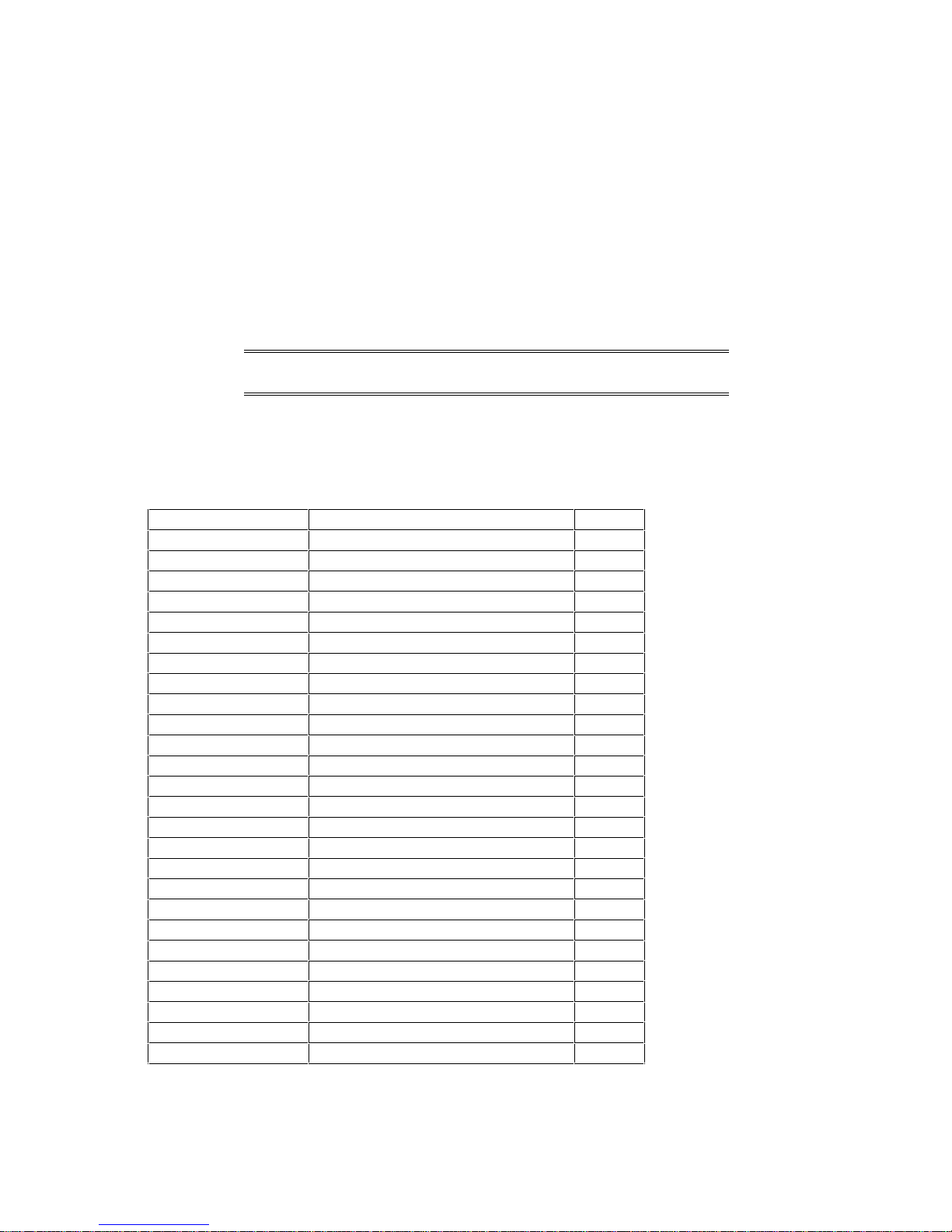
System Memory Map
00000h - 9FFFFh 640 KB–Base Memory Area
A0000h - BFFFFh 128 KB–Video Memory
C0000h - C7FFFh 32 KB–Video BIOS
C8000h - DFFFFh 96 KB–Accessory Boards Memory
E0000h - E7FFFh 32 KB–Available
E8000h - EFFFFh Reserved
F0000h - FFFFFh 64 KB–System BIOS
100000h - FFFFFFFFh 1 MB plus–Extended Memory
NOTE Reserved memory used by accessory boards must
be located in the area from C8000h to EFFFFh.
BIOS I/O PORT MAP
This section describes the HP BIOS port map. The next section provides more details about
how the BIOS uses the system board components mentioned in the I/O port list.
I/O Address Ports Function Bits
0000-000F DMA Controller 1 8
0020-0021 Interrupt Controller 1 8
0040-0043 Interval Timer 1 8
0060, 0064 Keyboard Controller 8
0061 NMI Status and Control 8
0070 NMI Mask register, RTC address 8
0071 RTC data 8
0081-0083, 008F DMA Low Page register 8
0092 Alternate reset and A20 Function 8
0096-009F Internal Ports 8
00A0-00A1 Interrupt Controller 2 8
00C0-00DF DMA Controller 2 8
00F0-00FF Co-processor error
0170-0177 Secondary IDE Controller
01F0-01F7 IDE Controller
0278-027F Parallel Port 3
02E8-02EF Serial Port 4
02F8-02FF Serial Port 2
0370-0377 Secondary Flexible Disk Controller
0378-037F Parallel Port 2
03B0-03DF Video
03BC-03BF Parallel Port 1
03E8-03EF Serial Port 3
03F0-03F7 Flexible Disk Controller
03F8-03FF Serial Port 1
0CF8-0CFF Used for PCI Configuration**
*These addresses are dedicated to configuration registers for PCI devices.
Page 24
ADDRESSING SYSTEM BOARD COMPONENTS
This section provides more details of how the BIOS uses the system board components
mentioned in the I/O port list.
DMA Channel Controllers
The system controller supports seven DMA channels, each with a page register used to extend
the addressing range of the channel to 16 MB. The only types of DMA transfer allowed are:
“I/O-to-memory” and “memory-to-I/O”
“I/O-to-I/O” and “memory-to-memory” transfers are disallowed by the hardware configuration.
The following table summarizes how the DMA channels are allocated.
First DMA controller (used for 8-bit transfers)
Channel Function
0 Available
1 Available or ECP mode for parallel port
2 Flexible disk I/O
3 Available or ECP mode for parallel port
Second DMA controller (used for 16-bit transfers)
Channel Function
4 Cascade from first DMA controller
5-6 Available
6-7 Available
Page 25
Interrupt Controllers
The system has two 8259A compatible interrupt controllers. They are arranged as a master
interrupt controller and a slave that is cascaded through the master.
The following table shows how the master and slave controllers are connected. The Interrupt
Requests (IRQ) are numbered sequentially, starting with the master controller, and followed by
the slave.
IRQ (Interrupt Vector) Interrupt Request Description
IRQ0(08h) System timer
IRQ1(09h) Keyboard controller
IRQ2(0Ah) Slave IRQ Cascade connection from INTC2 (Interrupt Controller 2)
IRQ8(70h) Real time clock
IRQ9(71h) Available for PCI accessory boards, if not used by ISA boards
IRQ10(72h) Available for PCI accessory boards, if not used by ISA boards
IRQ11(73h) Available for PCI accessory boards, if not used by ISA boards
IRQ12(74h) Mouse
IRQ13(75h) Pentium
IRQ14(76h) Primary channel of IDE controller
IRQ15(77h) Free, if not used by secondary channel of IDE controller*
IRQ3(0Bh) Free, if not used used for serial port**
IRQ4(0Ch) Free, if not used used for serial port**
IRQ5(0Dh) Free, if not used used for parallel port***
IRQ6(0Eh) Flexible disk drive controller
IRQ7(0Fh) Free, if not used used for parallel port***
*IRQ 15 can be made available by disabling the secondary channel of the IDE controller in the
SETUP program.
**IRQ3 and IRQ4 can be made available by disabling the serial ports in the SETUP program.
**IRQ5 and IRQ7 can be made available by disabling the parallel ports in the SETUP program.
PCI Interrupt Request Lines
PCI devices generate interrupt requests using up to four PCI interrupt request lines (INTA#,
INTB#, INTC#, and INTD#).
When a PCI device makes an interrupt request, the request is re-directed to the system
interrupt controller. The interrupt request will be re-directed to one of the IRQ lines made
available for PCI devices.
All PCI devices with interrupt transfer support will use and share INTA#. A multiple-function
PCI device may support several INT lines. These devices will require more than one system
interrupt request line.
Page 26

3 DESKTOP MANAGEMENT INTERFACE
This chapter describes an important feature of HP’s new style BIOS, the Desktop Management
Interface or DMI.
DMI INFORMATION STRUCTURE
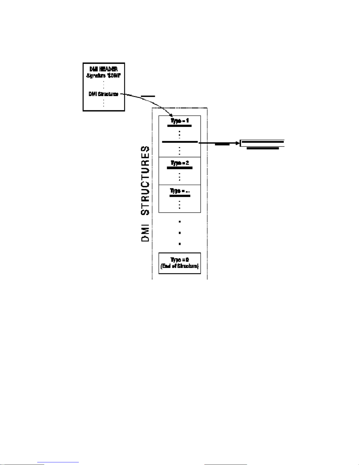
This BIOS presents a new method for storing and accessing information about the PC, called
the Desktop Management Interface or DMI.
The system administrator uses the DMI to access information about the PC, such as the BIOS
version number, the serial number, the processor type, and the size of the hard disk drive. This
information is stored in the Management Information Format Database, or MIF.
Pointers are used to indicate the position of a table or a string value. The following rules apply
to pointers:
• Pointers must never be zero. For empty strings, the pointer must point to a null (zero)
value.
• Far pointers are in Intel (little endian) format, with the segment in the high word and the
offset in the low word.
All string values are terminated by a null (zero) value.
Page 27
Overview of the DMI Information Structure
ACCESSING BIOS DMI INFORMATION
To access BIOS information, do the following steps:
1 Locate the DMI header.
Search for the “$DMI” signature in the segment E0000:0 or F0000:0.
2 Verify the checksums.
Refer to "Verifying the DMI Information Structure," in this chapter.
3 Locate the first sub-structure table using the far pointer given in the DMI header.
4 Walk through the tables to locate the desired table.
Each table is identified by a unique type. The type is given by the first byte of the table.
The length of the table is given by the second byte. The next table follows immediately
after the current one.
Page 28
5 Read off the required values.
Value
“$DMI”
00010010 (Ver 1.2)
0Eh
Far pointer (variable)
variable
variable
variable
Each type of table has a pre-defined format. For a list of the major table types, refer to
"DMI Sub-Structure Tables," in this chapter.
6 Use the pointer to retrieve string values.
All string values are terminated by a null (zero) value.
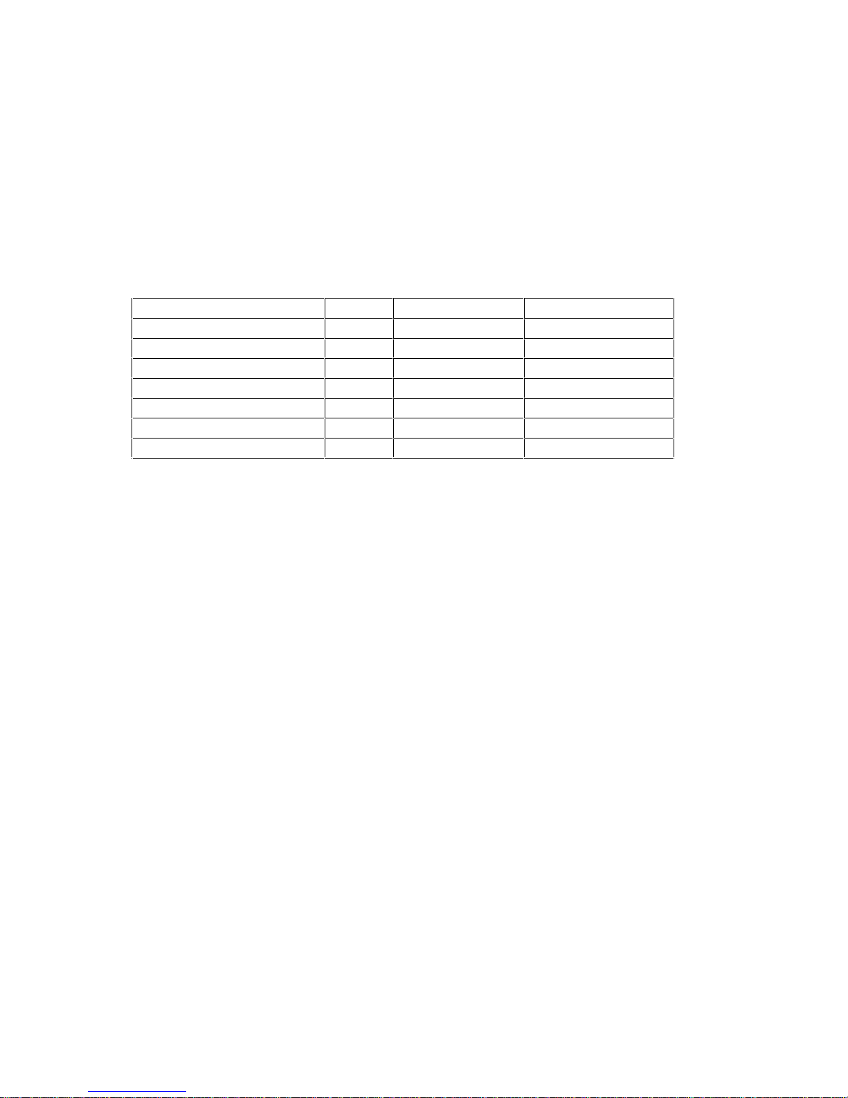
THE DMI HEADER
The DMI header is the starting point for all DMI information.
Field Offset Length
DMI Header Signature 0h 4 bytes
Version 4h 1 byte
DMI Header Length 5h 1 byte
Pointer to DMI structures 0Ah 4 bytes (DWORD)
Length of DMI structures 0Ch 2 bytes (WORD)
Checksum of DMI structures 0Ch 1 byte
Checksum of DMI header 0Dh 1 byte
VERIFYING THE DMI INFORMATION STRUCTURE
Before accessing the DMI tables, the checksums must be verified to ensure the reliability of the
information. To calculate a checksum value of a structure, do the following steps:
1 Add together all the bytes of the structure.
2 Convert the value to negative.
3 Cast the value to a byte (take the low byte).
There are two checksums, one for the DMI header and another for the remaining DMI structure.
To verify these two checksums, do the following steps:
1 Locate the DMI header.
2 Using the length value of the DMI header, calculate the checksum value for the DMI
header. (When adding together the bytes of the header, exclude the checksum byte, offset
0Dh.)
3 Verify this value against the checksum given for the DMI header.
4 Retrieve the position and length of the DMI structures.
5 Calculate the checksum value for the DMI structures.
6 Verify this value against the checksum given for the DMI structures.
Page 29
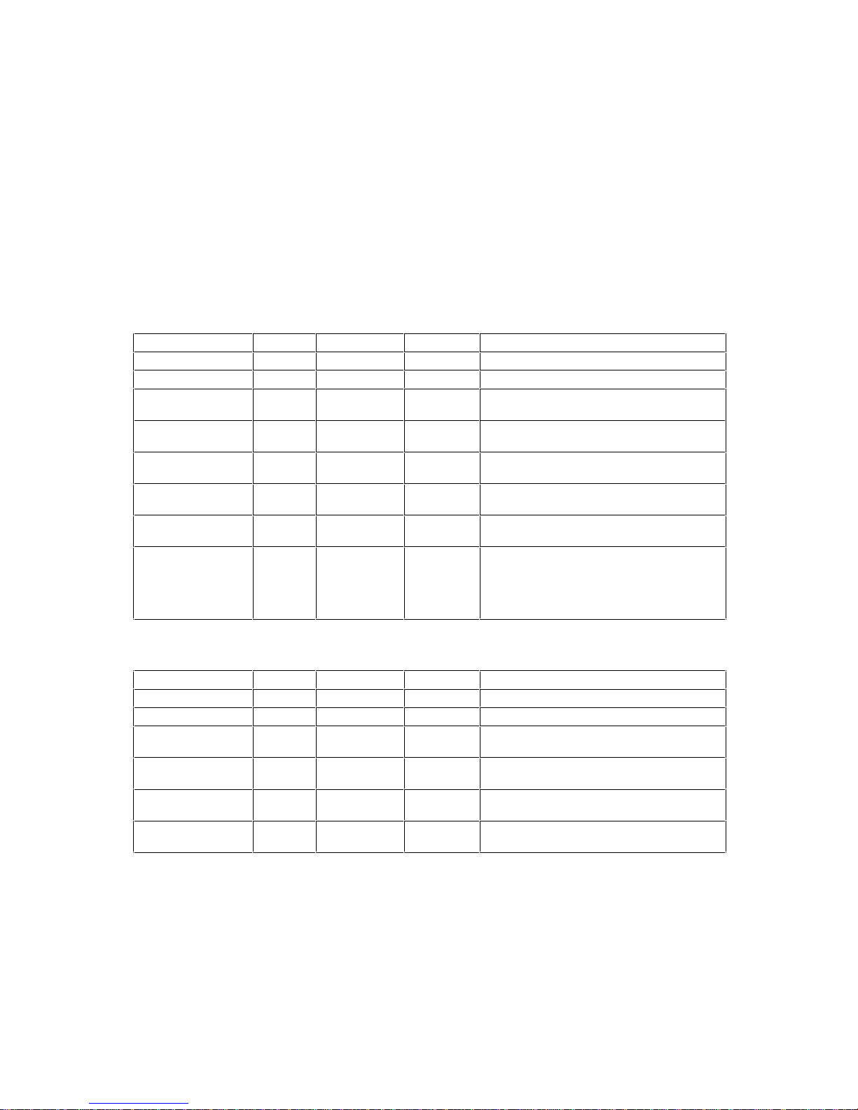
DMI SUB-STRUCTURE TABLES
Each type of table has a pre-defined format. Although the structure can evolve over time, new
fields are always added to the end of the table and the length value reflects this new size.
To parse several tables in order to find a specific table, simply use the table length. Using this
method will ensure that the parser can function even when the tables evolve over time.
To locate specific BIOS information, use the DMI sub-structure tables which are listed on the
following pages.
Type 1 : BIOS Information
Field Offset Length Value Description
Type 0h 1 byte 1 BIOS information table
Length 1h 1 byte 15h Table length (in bytes)
Vendor 2h 4 bytes
BIOS Version 6h 4 bytes
BIOS Starting
Address
BIOS Release Date Ch 4 bytes
BIOS
Characteristics
BIOS ROM Size 14h 1 byte variable Value indicating the size of the BIOS ROM:
Ah 2 bytes
10h 4 bytes
(DWORD)
(DWORD)
(WORD)
(DWORD)
(DWORD)
variable Far pointer to string containing BIOS vendor
variable Far pointer to string containing BIOS version
variable Segment location of BIOS starting address,
variable Far pointer to string containing BIOS release
variable
bit field
name.
number.
i.e. E800h.
date.
Bit field value indicating which functions the
BIOS supports.
0 → 64K,
1 → 128K,
2 → 256K,
3 → 512K, etc.
Type 2: Component ID
Field Offset Length Value Description
Type 0h 1 byte 2 Component ID table
Length 1h 1 byte 0Ah Table length
Manufacturer 2h 2 bytes
Product 4h 2 bytes
Version (oard
Revision)
Serial Number 8h 2 bytes
6h 2 bytes
(WORD)
(WORD)
(WORD)
(WORD)
variable Near pointer to string containing
manufacturer’s name.
variable Near pointer to string containing product
name.
variable Near pointer to string containing date code.
variable Near pointer to string containing serial
number.
Page 30
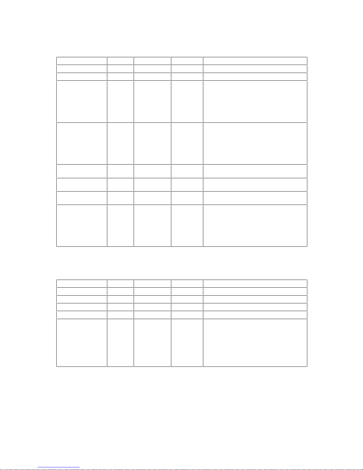
Type 3: Processor Information
Field Offset Length Value Description
Type 0h 1 byte 3 Processor information table
Length 1h 1 byte 0Bh Table length
Processor Type 2h 1 byte ENUM Value indicating processor type:
Processor Family 3h 1 byte ENUM Value indicating processor family:
Processor
Manufacturer
Processor Version 6h 2 bytes
Max Speed 8h 2 bytes
Processor Upgrade Ah 1 byte ENUM Value indicating processor upgrade type:
4h 2 bytes
(WORD)
(WORD)
(WORD)
variable Near pointer to string containing processor
variable Near pointer to string describing the
variable Decimal value of maximum processor speed.
1 → Other
2 → Unknown
3 → Central Processor
4 → Math Processor
5 → DSP Processor
6 → Video Processor
1 → Other
2 → Unknown
6 → 80486
A → 80487
B → Pentium
20 → Power PC
manufacturer’s name.
processor.
Example: 66d for a 66 MHz processor.
1 → Other
2 → Unknown
3 → Daughter Board
4 → ZIF Socket
5 → Replaceable Piggy Back
6 → None
HP-Specific DMI Sub-Structure Structures
Type 80h: HP ID
Field Offset Length Value Description
Type 0h 1 byte 80h HP ID information table
Length 1h 1 byte 6 Table length
Signature 02h 2 “HP” Hewlett-Packard signature
PC ID 04h 1 byte variable PC Identification
Capabilities 05h 1 byte BITMAP
Bit 7=1 → Tatooing supported
Bit 6=1 → PCMCIA device is present
Bit 5=1 → Infrared is present
Bit 4=1 → Two embedded serial ports present
Bit 3=1 → Mini-Tower (1) or Desktop (0)
Bit 2=1 → Embedded LAN present
Bit 1=1 → Using integrated video
Bit 0=1 → Supports HP LAN boot ROM
Page 31
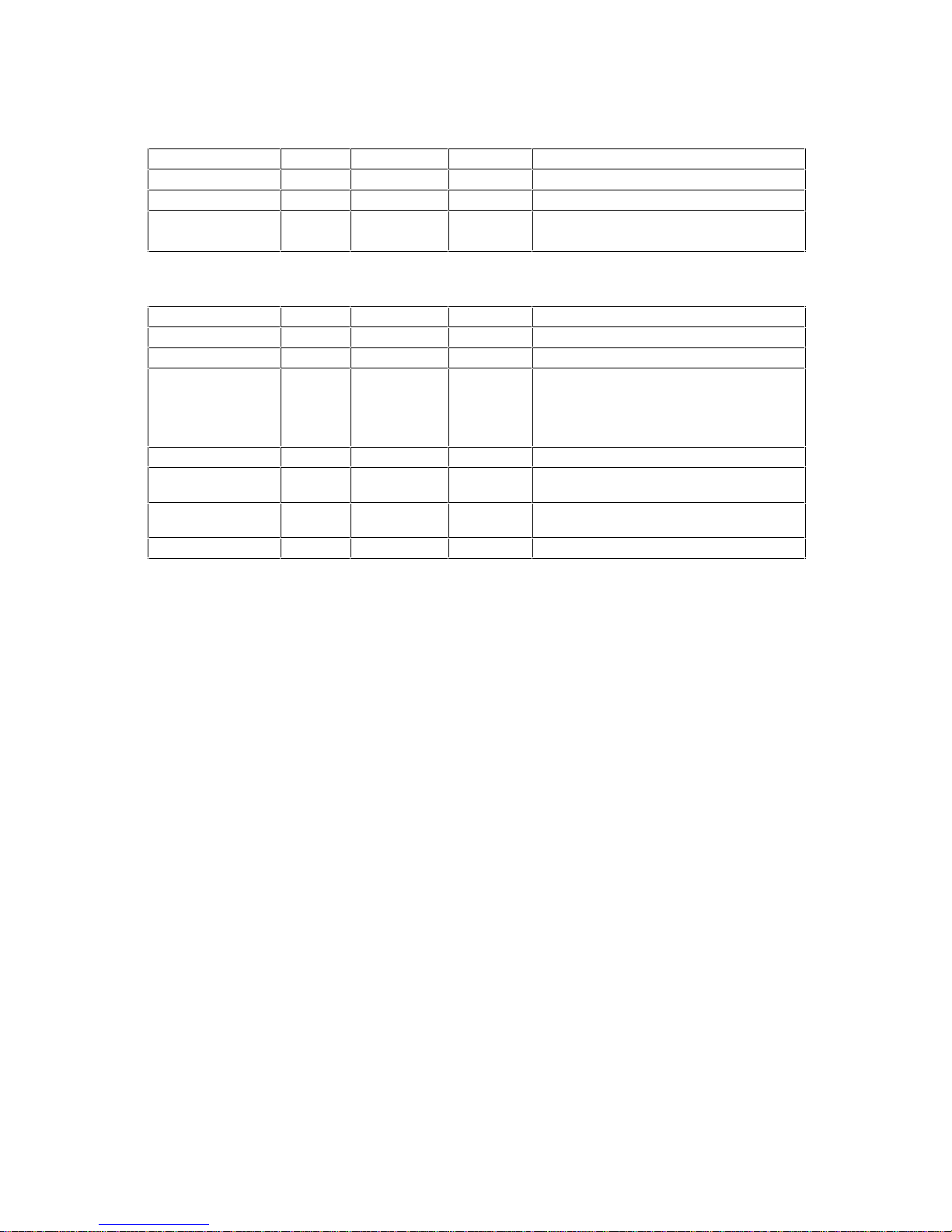
Type 81h: HP Configuration ID
Field Offset Length Value Description
Type 0h 1 byte 81h HP Configuration table
Length 1h 1 byte 3 Table length
Serial/Parallel
Count
02h 1 byte variable
Bits 7-4 → Number of integrated parallel ports
Bits 3-0 → Number of integrated serial ports
Type 84h: HP System Information
Field Offset Length Value Description
Type 0h 1 byte 84h HP system information table
Length 1h 1 byte Eh Table length
System Power-on
Time
Base Memory Size 04h 2 bytes variable Size of base memory in kilobytes
Extended Memory
Size
HP BIOS Version 08h 4 bytes variable Long pointer to string describing HP BIOS
CPU Name 0Ch 2 bytes variable Short pointer to string describing CPU name
02h 2 bytes variable Short pointer to string containing date and
time of last boot.
Format: “ccyymmddHHMM”
The value “************” indicates RTC has
failed.
06h 2 bytes variable Extended Memory size in 64 KB blocks
version
Page 32
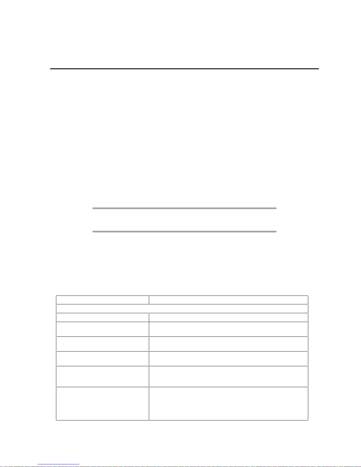
4 POWER-ON SELF-TESTS AND ERROR
MESSAGES
This chapter describes the power-on self-tests (POST), which are contained in the PC’s ROM
BIOS, and the error messages which can result.
POWER-ON SELF TEST (POST)
Each time the system is powered on, or a reset is performed, the POST is executed. The
POST process verifies the basic functionality of the system components and initializes certain
system parameters. The POST performs the tests in the order described in this chapter.
The POST displays a graphic screen with the HP Vectra logo. If the POST detects an error, the
error message is displayed. To see the tests performed during the POST, press [ESC] when
the HP Vectra logo appears and the display will switch to text mode. In this mode, a summary
configuration screen will be displayed at the end of the POST. Pressing the PAUSE/ BREAK
key at any time will allow you to inspect the screen contents. Press any key to resume
If the POST is initiated by a soft reset [CTRL] [ALT] and [DELETE], the RAM tests are not
executed and shadow RAM is not cleared. In all other respects, the POST executes in the
same way following power-on or a soft reset.
NOTE The POST does not detect when a
drive
(“HDD 1” or “HDD 3” in the setup) has been
slave hard disk
installed or changed.
SHADOW RAM
On HP personal computers, access to certain ROM data is enhanced by using shadow RAM.
During the POST, the BIOS and other ROM data is copied into high-speed shadow RAM. The
shadow RAM is addressed at the same physical location as the original ROM in a manner
which is completely transparent to applications. This technique provides faster access to the
system BIOS firmware.
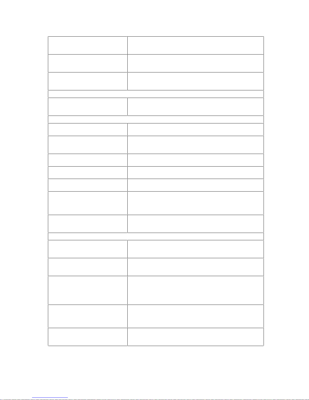
POST Test Description
System BIOS Tests
LED Test
Processor Test
System (BIOS) ROM Test
RAM Refresh Timer Test
Interrupt RAM Test
Shadow the System ROM BIOS
Tests the LEDs on the control panel.
Tests the processor’s registers. Test failure causes the boot
process to abort.
Calculates an 8-bit checksum. Test failure causes the boot
process to abort.
Tests the RAM refresh timer circuitry. Test failure causes the
boot process to abort.
Checks the first 64 KB of system RAM used to store data
corresponding to various system interrupt vector addresses.
Test failures cause the boot process to abort.
Tests the system ROM BIOS and shadows it. Failure to
shadow the ROM BIOS will cause an error code to display.
The boot process will continue, but the system will execute
from ROM. This test is not performed after a soft reset (using
[CTRL] [ALT] and [DELETE]).
Page 33
Load CMOS Memory
CMOS RAM Test
Internal Cache Memory Test
Initialize the Video
Test External Cache
Shadow SCSI ROM
8042 Self-Test
Timer 0/Timer 2 Test
DMA Subsystem Test
Interrupt Controller Test
Real-Time Clock Test
RAM Address Line
Independence Test
Size Extended Memory
Real-Mode Memory Test (First
640KB)
Shadow RAM Test
Protected Mode RAM Test
(Extended RAM)
Checks the serial EEPROM and returns an error code if it has
been corrupted. Copies the contents of the EEPROM into
CMOS RAM.
Checks the CMOS RAM for start-up power loss, verifies the
CMOS RAM checksum(s). Test failure causes error codes to
display.
Tests the processor’s internal level-one cache RAM. Test
failure causes an error code to display and the boot process
to abort.
Video Tests
Initializes the video subsystem, tests the video shadow RAM,
and, if required, shadows the video BIOS. A failure causes an
error code to display, but the boot process continues.
System Board Tests
Tests the level-two cache. A failure causes an error code to
display and disables the external cache.
Tests for the presence of HP SCSI ROMs. If SCSI ROMs are
detected, their contents are copied into the shadow RAM area.
A failure will cause an error code to display.
Downloads the 8042 and invokes the 8042 internal self-test. A
failure causes an error code to display.
Tests Timer 0 and Timer 2. Test failure causes an error code
to display.
Checks the DMA controller registers. Test failure causes an
error code to display.
Tests the Interrupt masks, the master controller interrupt path
(by forcing an IRQ0), and the industry-standard slave
controller (by forcing an IRQ8). Test failure causes an error
code to display.
Checks the real-time clock registers and performs a test that
ensures that the clock is running. Test failure causes an error
code to display.
Memory Tests
Verifies the address independence of real-mode RAM (no
address lines stuck together). Test failure causes an error
code to display.
Sizes and clears the protected mode (extended) memory and
writes the value into CMOS bytes 30h and 31h. If the system
fails to switch to protected mode, an error code is displayed.
Read/write test on real-mode RAM. (This test is not done
during a reset using [CTRL] [ALT] and [DELETE]). The test
checks each block of system RAM to determine how much is
present. Test failure of a 64 KB block of memory causes an
error code to display, and the test is aborted.
Tests shadow RAM in 64 KB segments (except for segments
beginning at A000h, B000h, and F000h). If they are not being
used, segments C000h, D000h and E000h are tested. Test
failure causes an error code to display.
Tests protected RAM in 64 KB segments above 1 MB. (This
test is not done during a reset using [CTRL] [ALT] and
[DELETE]). Test failure causes an error code to display.
Page 34
Keyboard Test
Mouse Test
Flexible Disk Controller
Subsystem Test
Internal Numeric Coprocessor
Test
Parallel Port Test
Serial Port Test
Hard Disk Controller
Subsystem Test
System Generation
Plug and PlayConfiguration
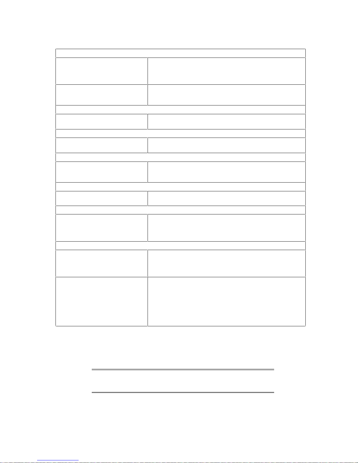
Keyboard / Mouse Tests
Invokes a built-in keyboard self-test of the keyboard’s
microprocessor and tests for the presence of a keyboard and
for stuck keyboard keys. Test failure causes an error code to
display.
If a mouse is present, invokes a built-in mouse self-test of the
mouse’s microprocessor and for stuck mouse buttons. Test
failure causes an error code to display.
Tests of Flexible Disk Drive A
Tests for proper operation of the flexible disk controller. Test
failure causes an error code to display.
Coprocessor Tests
Checks for proper operation of the numeric coprocessor part
of the processor. Test failure causes an error code to display.
Parallel Port Tests
Tests the integrated parallel port registers, as well as any
other parallel ports. Test failure causes an error code to
display.
Serial Port Tests
Tests the integrated serial port registers, as well as any other
serial ports. Test failure causes an error code to display.
Hard Disk Drive Tests
Tests for proper operation of the hard disk controller. Test
failure causes an error code to display. The test does not
detect hard disk replacement or changes in the size of the
hard disk.
System Configuration Tests
Initiation of the system generation (SYSGEN) process, which
compares the configuration information stored in the CMOS
memory with the actual system. If a discrepancy is found, an
error code will be displayed.
Configures any Plug and Play device detected (either PCI or
ISA):
• All PCI devices, and any ISA device necessary for loading
the operating system will be configured for use.
• Any ISA device that is not required for loading the
operating system, will be initialized (prepared for loading of
a device driver), but not fully configured for use.
ERROR MESSAGES
When the PC is switched on or reset, a power-on hardware test is performed. If an error occurs,
an error message is displayed.
NOTE HP’s new style BIOS does not display POST error
codes (such as 910B) which existed in the BIOS of
previous HP Vectra PCs.
Page 35

Message Corrective Action and/or Explanation
Operating system not found Check whether the disk, HDD, FDD or CD-ROM disk drive is
connected.
If it is connected, check that it is detected by Setup.
Check that your boot device is enabled on the Setup Security
menu.
If the problem persists, check that the boot device contains the
operating system.
Missing operating system If you have configured HDD user parameters, check that they
are correct. Otherwise, use HDD type “Auto” parameters.
Failure fixed disk
(preceded by a 30” time-out)
Check that HDD is connected.
Check that HDD is detected in Setup.
Check that boot on hard disk drive is enabled in Setup.
Diskette Drive A (or B) error Check whether the diskette drive is connected.
Check Setup for the configuration.
System battery is dead You may get this message if the PC is disconnected for a few
days. When you Power-on the PC, run
Setup
to update the
configuration information. The message should no longer be
displayed. Should the problem persist, replace the battery.
Keyboard error Check that the keyboard is connected.
Resource Allocation Conflict - PCI
Clear CMOS.
device 0079 on motherboard
Video Plug and Play interrupted or
failed Re-enable in Setup and try
You may have powered your PC Off/On too quickly and the PC
turned off Video plug and play as a protection.
again
System CMOS checksum bad -
run Setup
CMOS contents have changed between 2 power-on sessions.
Run Setup for configuration.
I/O device IRQ conflict Serial ports A and B may have been assigned the same IRQ.
Assign a different IRQ to each serial port and save the
configuration.
No message, system “hangs”
after POST
Check that cache memory and main memory are correctly set
in their sockets.
Other An error message may be displayed and the PC may “hang” for
20 seconds and then beep. The POST is probably checking for
a mass storage device which it cannot find and the PC is in
Timeout Mode. After Timeout, run Setup to check the
configuration.
Page 36
BEEP CODES
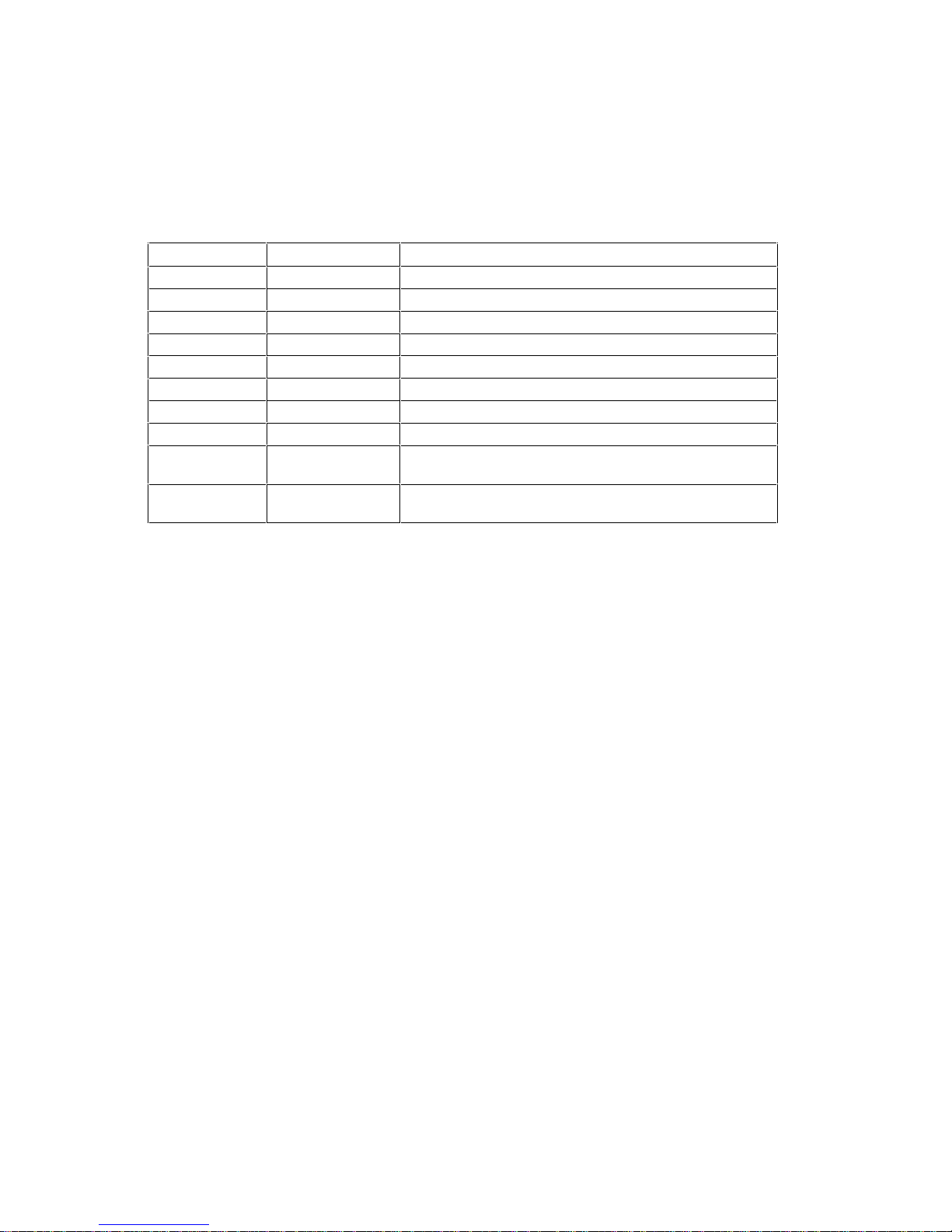
If a terminal error occurs during POST, the system issues a beep code before attempting to
display the error. Beep codes are useful for identifying the error when the system is unable to
display the error message.
Beep Code* Numeric Code Description
1-2-2-3 16h BIOS ROM checksum failure
1-3-1-1 20h DRAM refresh test failure
1-3-1-3 22h 8742 Keyboard controller test failure
1-3-4-1 2C RAM failure
1-3-4-3 2E RAM failure on data bits in low byte of memory bus
1-4-1-1 30 RAM failure on data bits in high byte of memory bus
2-1-2-3 46 ROM copyright notice check failure
2-2-3-1 58 Unexpected interrupts test failure
1-2 98 Video configuration failure or
Option ROMs checksum failure
1 B4 This does not indicate an error.
There is one short beep before system startup.
*Values indicate number and relative length of beep signals. For example, 1-2-2-3 is one long beep,
followed by two short beeps, followed by another two short beeps, and finally three short beeps.
Page 37
5 THE ULTRA VGA VIDEO CONTROLLERS
Memory
2 MB
This chapter gives details of the Video Subsystems used by the HP Vectra VL 5/xx Series 4
PCs.
Basic models have the Trio S3 video controller integrated on the system board. Other models
have a Matrox MGA Millennium video adapter board installed in a PCI slot.
THE MATROX MGA MILLENNIUM VIDEO ADAPTER BOARD
The Matrox MGA Millennium video adapter board has 2 MB video memory installed on the
board, a VESA feature connector, and a socket for either a video memory upgrade module or
an MPEG upgrade module.
The video adapter board uses the PCI bus for data transfers between the processor and the
video subsystem, and has the following features:
• 100% compatible with IBM® VGA display standard
• 64-bit video memory access
• Hardware acceleration of graphical user interface (GUI) operations
• Support for up to 8 MB WRAM (Window RAM) at 60 ns
• Graphics resolutions of up to 1600 x 1200
• Integrated 24-bit RAMDAC
• Green PC power saving features
• Standard and Enhanced Video Graphics Array (VGA) modes
• DDC 2B compliant.
VIDEO MEMORY
The Matrox MGA Millennium has 2 MB of video WRAM (window random access memory)
preinstalled on the video adapter board, and has a socket for the attachment of a video
memory upgrade card or an MPEG upgrade card. The video memory upgrade card provides
an extra 2 or 6 MB of video memory, for a total of 4 MB or 8 MB video WRAM. (The 8 Mb
video upgrade is available only from Matrox Electronic Systems Limited.)
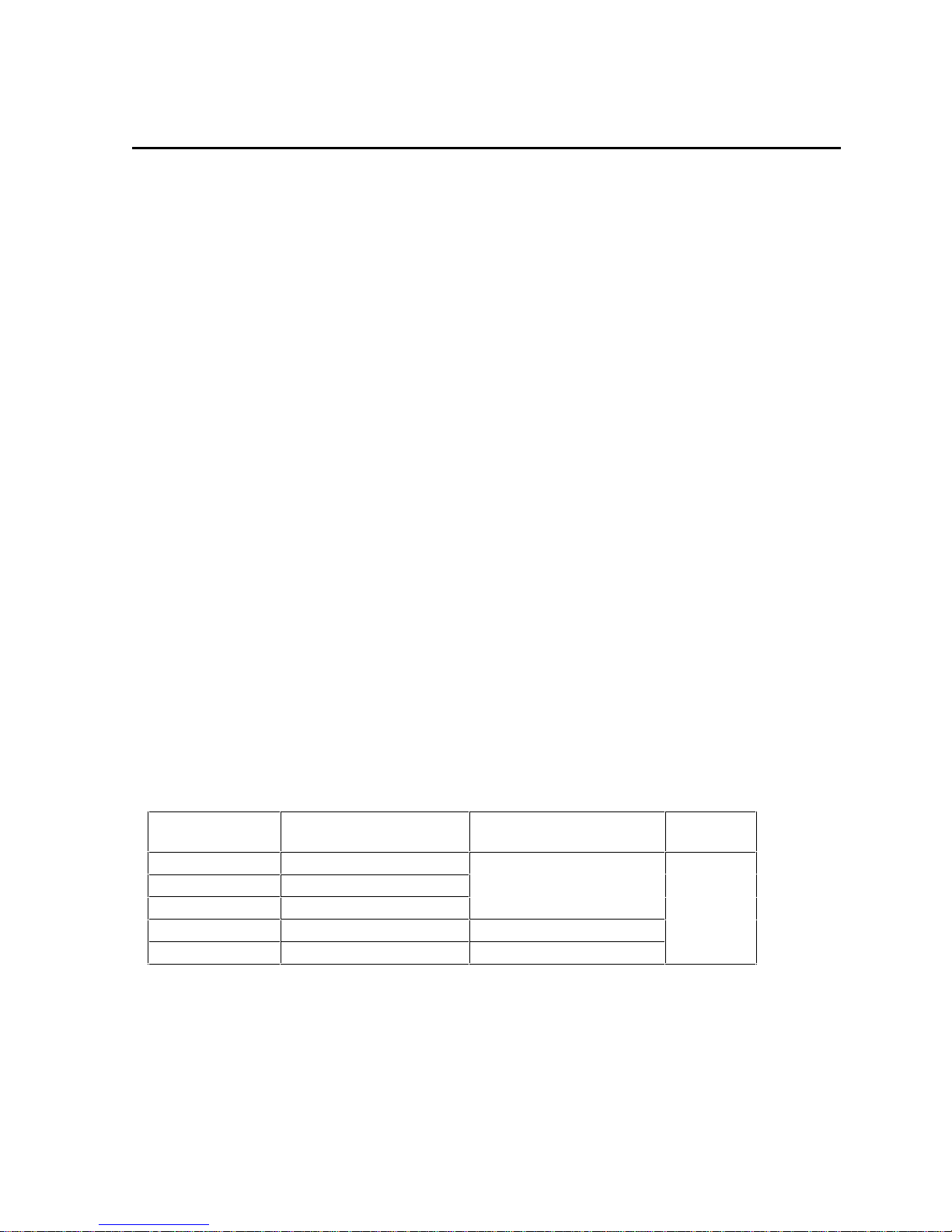
AVAILABLE VIDEO RESOLUTIONS
Resolution Number of colors Video Adapter Maximum
Refresh Rate (Hz)
640 x 480 256, 64K, 16M 120
800 x 600 256, 64K, 16M
1024 x 768 256, 64K
1280 x 1024 256 100
1600 x 1200* 256 72
*Upper limit of refresh rate for HP monitors is 60Hz at this resolution.
Page 38
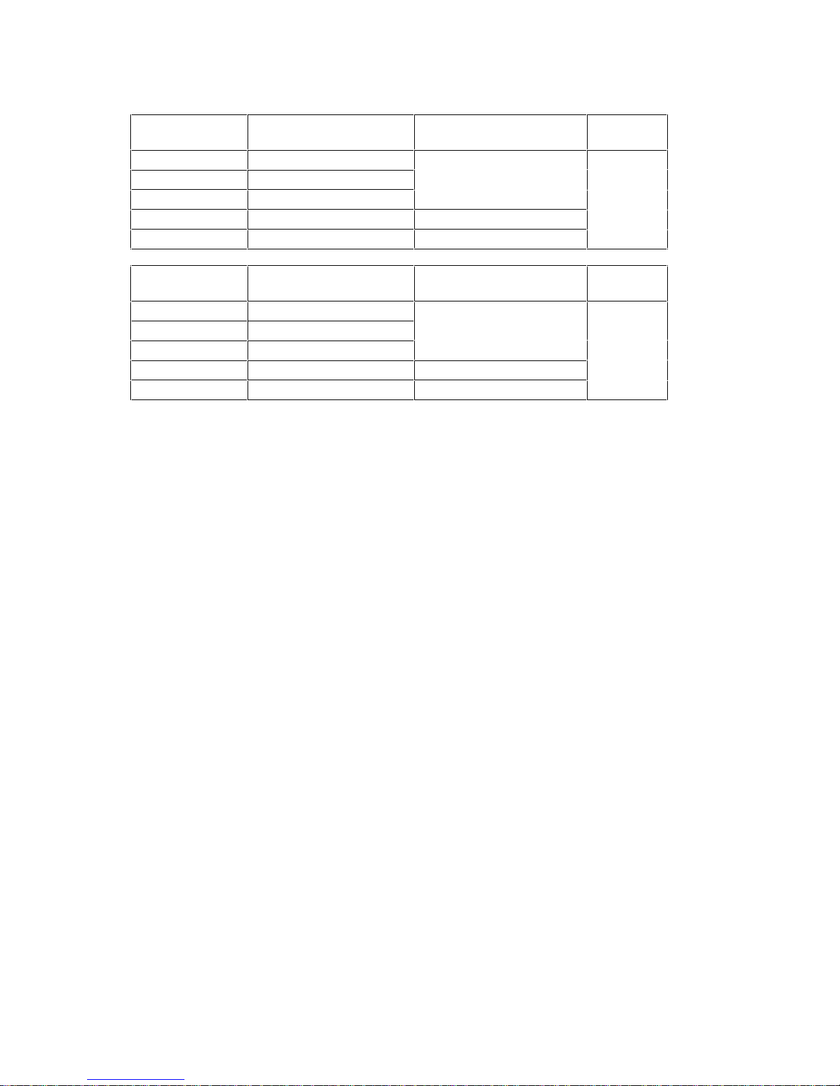
Video Adapter Maximum
Memory
4 MB
Memory
8 MB
Resolution Number of colors
640 x 480 256, 64K, 16M 120
800 x 600 256, 64K, 16M
1024 x 768 256, 64K
1280 x 1024 256, 64K, 16M (24 bpp) 100
1600 x 1200* 256, 64K 72
Resolution Number of colors
640 x 480 256, 64K, 16M 120
800 x 600 256, 64K, 16M
1024 x 768 256, 64K, 16M
1280 x 1024 256, 64K, 16M 100
1600 x 1200* 256, 64K, 16M 72
*Upper limit of refresh rate for HP monitors is 60Hz at this resolution.
Refresh Rate (Hz)
Video Adapter Maximum
Refresh Rate (Hz)
VESA CONNECTOR
The Video Electronics Standards Association (VESA) defines a standard video connector,
variously known as the VESA
feature
connector. The Matrox MGA Millennium video adapter board supports an output-only VESA
feature connector in VGA mode. This connector is integrated on the adapter board, and is
connected directly to the pixel data bus and the synchronization signals.
connector,
auxiliary
connector, or
pass-through
FURTHER INFORMATION
For further information on the Matrox MGA Millennium video adapter board, contact Matrox
Electronic Systems.
Matrox Electronic Systems Ltd.
1055 St. Regis Blvd.
Dorval, Quebec
Canada H9P 2T4
Telephone: (514) 685-2630
Fax: (514) 685-2853
BBS: (514) 685-6008
THE INTEGRATED ULTRA VGA VIDEO CONTROLLER
The HP Vectra VL 5/xx Series 4 PCs provide an integrated Ultra VGA video subsystem,
comprising a S3 Trio family video controller and 1 MB DRAM. Two sockets are provided for
installation of an additional 1 MB (2×512 KB modules) DRAM.
Two versions of the S3 Trio video controllers are used: S3 Trio 765 64V+ and S3 Trio 764.
The drivers for these two video controllers are not compatible
provided for PC maintenance. Vectra models using the S3 Trio 765 64V+ controller have
product numbers D3xxxA, while the models using the S3 Trio 764 controller have product
numbers D3xxxB.
. Two different sets of drivers are
Page 39

The video subsystem uses the PCI bus for data transfers between the processor and the video
subsystem, and has the following features:
• 100% compatible with IBM® VGA display standard
• 32-bit video memory access with 1 MB DRAM. This increases to 64-bit access when an
additional 1 MB DRAM is installed
• Hardware acceleration of graphical user interface (GUI) operations
• Support for up to 2 MB DRAM at 60 ns
• Graphics resolutions of up to 1280 x 1024
• Integrated 24-bit RAMDAC
• Green PC power saving features
• Standard and Enhanced Video Graphics Array (VGA) modes
• DDC 1 compliant.
VIDEO MEMORY
The S3 Trio 765 64V+ integrated video subsystem has 1 MB of video DRAM preinstalled on
the system board, and provide two sockets for the installation of a pair of 512KB video DRAM
chips, giving a total of 2 MB video memory.
VIDEO MODES
The video subsystem is responsible for generating video data (which is placed in video
memory) to be sent to the display.
The following table details the standard VGA modes which are currently implemented in the
video BIOS. These modes are supported by standard BIOS functions; that is, the video BIOS
(which is mapped contiguously in the address range C0000h to C7FFFh) contains all the
routines required to configure and access the video subsystem.
Page 40
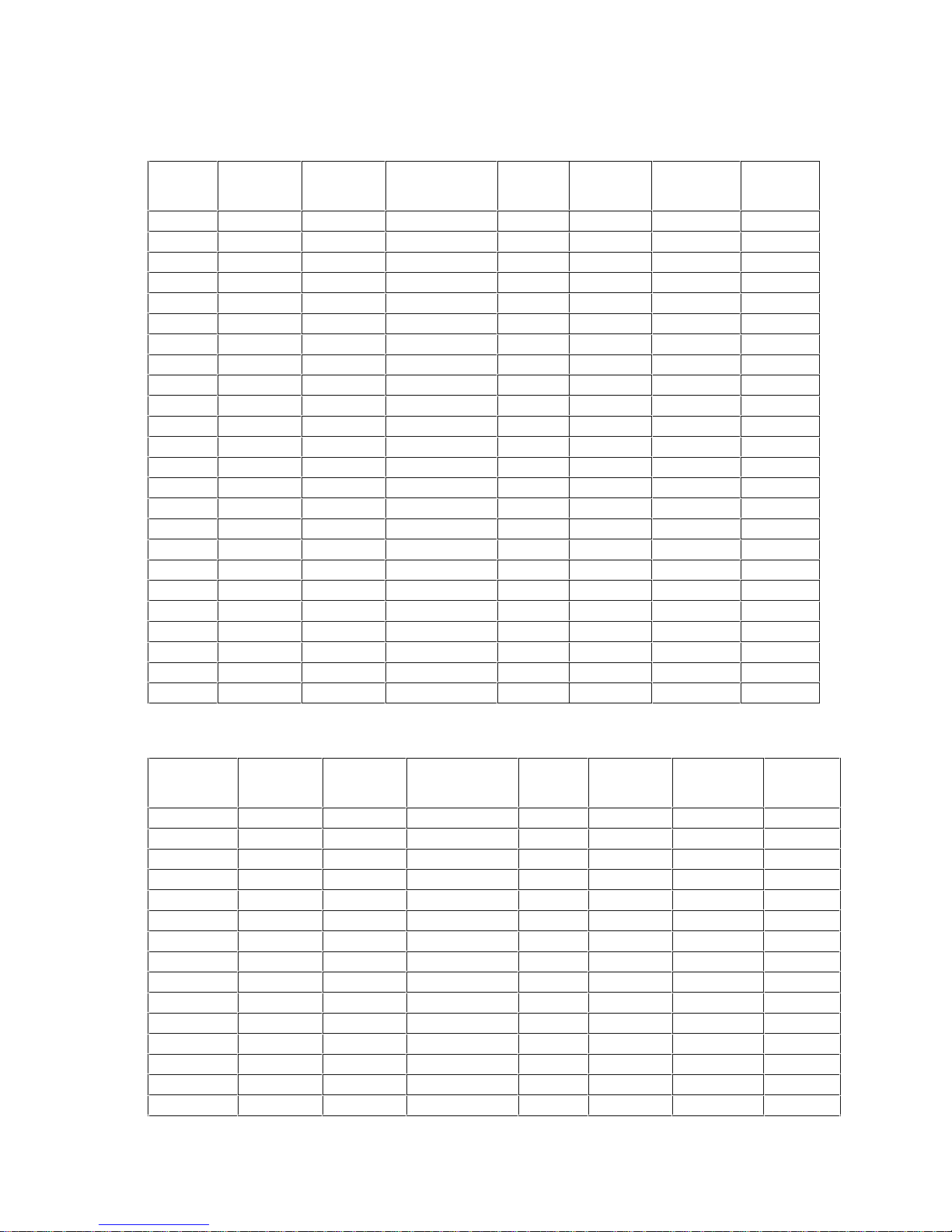
Standard VGA Modes
Horizontal
Refresh
(kHz)
55
47.7
63.7
31.5
31.5
31.5
31.5
12.540
12.540
12.540
31.5
31.5
37.9
37.5
45
Mode
No. Standard
00h VGA text 40 x 25 chars b/w 70 31.5 25.175
00h* VG A text 40 x 25 chars b/w 70 31.5 25.175
00h+ VGA text 40 x 25 chars b/w 70 31.5 28.322
01h VGA text 40 x 25 chars 16 70 31.5 25.175
01h* VG A text 40 x 25 chars 16 70 31.5 25.175
01h+ VGA text 40 x 25 chars 16 70 31.5 28.322
02h VGA text 80 x 25 chars b/w 70 31.5 25.175
02h* VG A text 80 x 25 chars b/w 70 31.5 25.175
02h+ VGA text 80 x 25 chars b/w 70 31.5 28.322
03h VGA text 80 x 25 chars 16 70 31.5 25.175
03h* VG A text 80 x 25 chars 16 70 31.5 25.175
03h+ VGA text 80 x 25 chars 16 70 31.5 28.322
04h VGA graph 320 x 200 4 7 0 31.5 25.175
05h VGA graph 320 x 200 4 7 0 31.5 25.175
06h VGA graph 640 x 200 2 7 0 31.5 25.175
07h VGA text 80 x 25 chars b/w 70 31.5 28.322
07h+ VGA text 80 x 25 chars b/w 70 31.5 28.322
0Dh VGA graph 320 x 200 16 70 31.5 25.175
0Eh VGA graph 640 x 200 16 70 31.5 25.175
0Fh VGA graph 640 x 350 b/w 70 31.5 25.175
10h VGA graph 640 x 350 16 70 31.5 25.175
11h VGA graph 640 x 480 2 6 0 31.5 25.175
12h VGA graph 640 x 480 16 60 31.5 25.175
13h VGA graph 320 x 200 256 70 31.5 25.175
Interface
Type
Resolution
No. of
Colors
Vertical
Refresh
(Hz)
Horizontal
Refresh
(kHz)
Dot
Clock
(MHz)
The extended modes supported by the video BIOS are:
Extended
Mode No.
4Eh 207h graph 1152 x 864 256 60
4Fh 208h graph 1280 x 1024 8 43i
4Fh 208h graph 1280 x 1024 8 60
51h 212h graph 640 x 480 16.7 M 60
52h 213h graph 640 x 400 16.7 M 70
54h 10Ah text 132 x 43 chars 16 70
55h 109h text 132 x 25 chars 16 70
65h 10Dh graph 320 x 200 32,768 70
66h 10Eh graph 320 x 200 65,536 70
67h 10Fh graph 320 x 200 16.7 M 70
68h 100h graph 640 x 400 256 70
69h 101h graph 640 x 480 256 60
69h 101h graph 640 x 480 256 72
69h 101h graph 640 x 480 256 75
69h 101h graph 640 x 480 256 85
VESA
Mode No.
Interface
Type
Resolution
No. of
Colors
Vertical
Refresh
(Hz)
Dot
Clock
(MHz)
80.000
80.000
110.000
25.000
25.000
40.000
40.000
25.175
25.175
31.500
31.500
36.000
Page 41
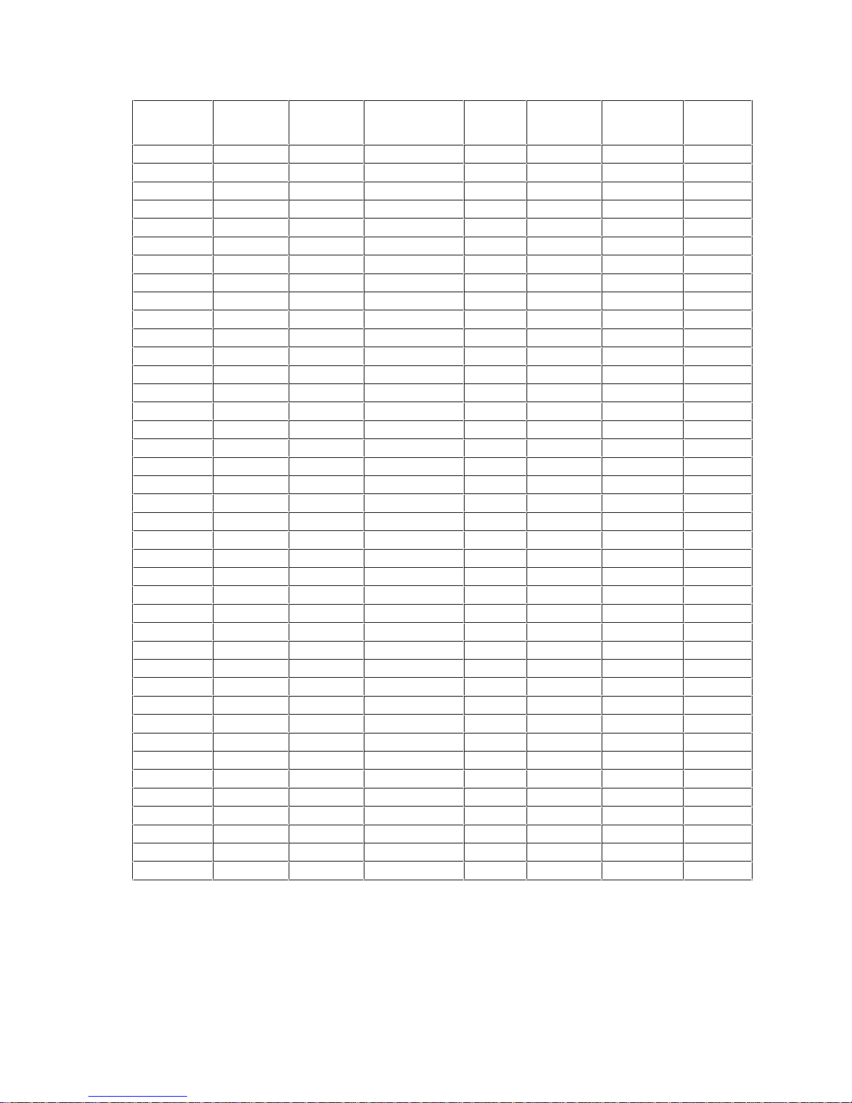
Extended
Horizontal
Refresh
(kHz)
37.9
48.1
47.5
53.6
37.9
48.1
46.8
53.6
35.5
48.4
56.5
60.2
68.7
35.5
48.4
56.5
60.0
68.7
46
31.5
37.5
37.5
45
31.5
37.5
37.5
45
31.5
37.9
37.5
45
37.9
48.1
46.8
53.6
37.9
48.1
46.8
53.6
Mode No.
6Ah 102h graph 800 x 600 16 60
6Ah 102h graph 800 x 600 16 72
6Ah 102h graph 800 x 600 16 75
6Ah 102h graph 800 x 600 16 85
6Bh 103h graph 800 x 600 256 60
6Bh 103h graph 800 x 600 256 72
6Bh 103h graph 800 x 600 256 75
6Bh 103h graph 800 x 600 256 85
6Ch 104h graph 1024 x 768 16 43i
6Ch 104h graph 1024 x 768 16 60
6Ch 104h graph 1024 x 768 16 70
6Ch 104h graph 1024 x 768 16 75
6Ch 104h graph 1024 x 768 16 85
6Dh 105h graph 1024 x 768 256 43i
6Dh 105h graph 1024 x 768 256 60
6Dh 105h graph 1024 x 768 256 70
6Dh 105h graph 1024 x 768 256 75
6Dh 105h graph 1024 x 768 256 85
6Eh 106h graph 1280 x 1024 16 45i
6Eh 106h graph 1280 x 1024 16 60 110.000
70h 110h graph 640 x 480 32,768 60
70h 110h graph 640 x 480 32,768 72
70h 110h graph 640 x 480 32,768 75
70h 110h graph 640 x 480 32,768 85
71h 111h graph 640 x 480 65,536 60
71h 111h graph 640 x 480 65,536 72
71h 111h graph 640 x 480 65,536 75
71h 111h graph 640 x 480 65,536 85
72h 112h graph 640 x 480 16.7 M 60
72h 112h graph 640 x 480 16.7 M 72
72h 112h graph 640 x 480 16.7 M 75
72h 112h graph 640 x 480 16.7 M 85
73h 113h graph 800 x 600 32,768 60
73h 113h graph 800 x 600 32,768 72
73h 113h graph 800 x 600 32,768 75
73h 113h graph 800 x 600 32,768 85
74h 114h graph 800 x 600 65,536 60
74h 114h graph 800 x 600 65,536 72
74h 114h graph 800 x 600 65,536 75
74h 114h graph 800 x 600 65,536 85
VESA
Mode No.
Interface
Type
Resolution
No. of
Colors
Vertical
Refresh
(Hz)
Dot
Clock
(MHz)
40.000
50.000
49.500
56.000
40.000
50.000
49.500
56.000
44.900
65.000
75.000
80.000
95.000
44.900
65.000
75.000
80.000
95.000
80.000
25.175
31.500
31.500
36.000
25.175
31.500
31.500
36.000
25.175
31.500
31.500
36.000
40.000
50.000
49.500
57.000
40.000
50.000
49.500
57.000
Page 42
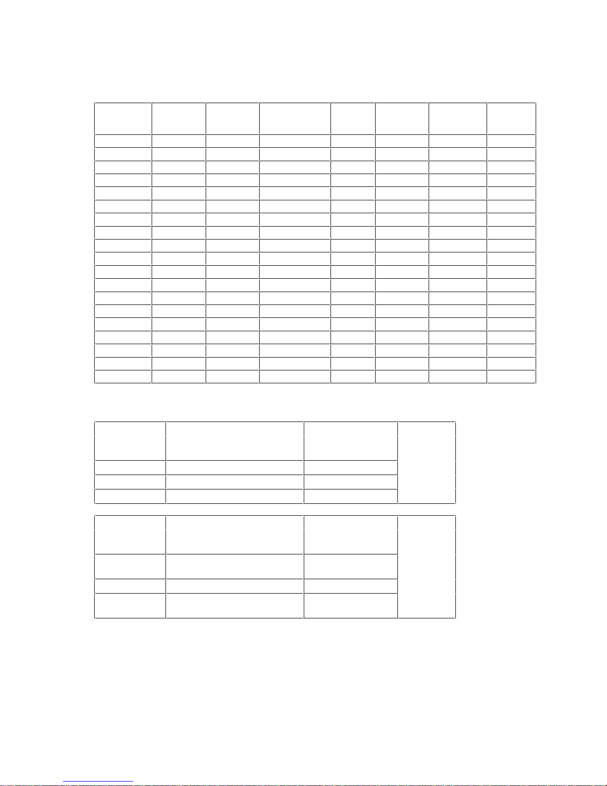
Extended Video Modes with 1 MB DRAM
Horizontal
Refresh
(kHz)
46
65
77.7
79.5
37.9
41.8
46.8
53.6
35
48.9
56.5
60.2
68.7
35
48.9
56.5
60.2
68.7
62.00
Extended
Mode No.
6Fh 107h graph 1280 x 1024 256 45i
6Fh 107h graph 1280 x 1024 256 60
6Fh 107h graph 1280 x 1024 256 72
6Fh 107h graph 1280 x 1024 256 75
75h 115h graph 800 x 600 16.7 M 60
75h 115h graph 800 x 600 16.7 M 72
75h 115h graph 800 x 600 16.7 M 75
75h 115h graph 800 x 600 16.7 M 85
76h 116h graph 1024 x 768 32,768 43i
76h 116h graph 1024 x 768 32,768 60
76h 116h graph 1024 x 768 32,768 70
76h 116h graph 1024 x 768 32,768 75
76h 116h graph 1024 x 768 32,768 85
77h 117h graph 1024 x 768 65,536 43i
77h 117h graph 1024 x 768 65,536 60
77h 117h graph 1024 x 768 65,536 70
77h 117h graph 1024 x 768 65,536 75
77h 117h graph 1024 x 768 65,536 85
7Ch 120h graph 1600 x 1200 256 48.5i
VESA
Mode No.
Interface
Type
Resolution
No. of
Colors
Vertical
Refresh
(Hz)
Dot
Clock
(MHz)
40.000
55.000
65.000
67.000
40.000
50.000
49.500
57.000
44.900
65.000
75.000
80.000
95.000
44.900
65.000
75.000
80.000
95.000
67.000
AVAILABLE BIOS VIDEO RESOLUTIONS
Resolution Number of colors Refresh Rate (Hz) Memory
640 x 480 16, 16M (24 bpp*)
256, 32K, 64K
800 x 600 16, 256, 32K, 64K 60, 72, 75
1024 x 768 16, 256 i43**, 60, 70, 75
1280 x 1024 16 i45**, 60
Resolution Number of colors Refresh Rate (Hz) Memory
640 x 480 16, 16M (24 bpp*)
256, 32K, 64K, 16M (32 bpp*)6060, 72, 75
800 x 600 16, 256, 32K, 64K,
16M (32 bpp*
1024 x 768 16, 256, 32K, 64K i43**, 60, 70, 75
1280 x 1024 16
256
*bpp = bits per pixel
**interlaced
60
60, 72, 75
60, 72, 75
i45**, 60
i45**, 60, 72, 75
1 MB
1 MB
Page 43
VESA CONNECTOR
The Video Electronics Standards Association (VESA) defines a standard video connector,
variously known as the VESA feature connector, auxiliary connector, or pass-through
connector. The integrated video controller supports an output-only VESA feature connector.
This connector is integrated directly on the system board, and is connected directly to the pixel
data bus and the synchronization signals.
To use the VESA feature connector in DOS, Windows 3.11 or Windows 95, the FCON.EXE
utility must be executed. This utility configures the system.
WARNING: Use of the VESA feature connector will disable
the 1 MB video memory upgrade, if one is
installed. Only the standard 1 MB of video
memory will be used.
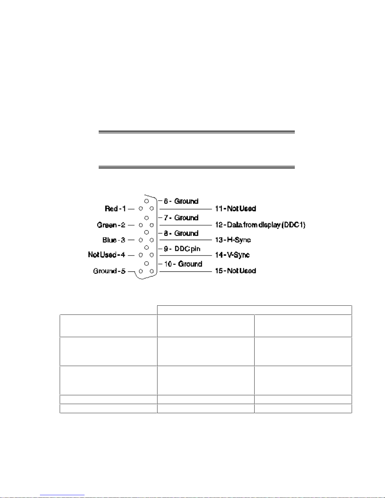
DB15 CONNECTOR PINOUT
VIDEO CONTROLLER SUMMARY
HP Vectra VL 5/xx Series 4 and HP Vectra VL 5/xx MT series 4
Video Controllers Integrated 64-bit Ultra VGA on
PCI bus
(S3 Trio 765 64V+or S3 Trio 764)
Hardware Acceleration of major
graphics operations to speed up
applications using graphical user
interfaces (GUIs)
DRAM support 1-2 MB of 60 ns
Graphics Resolutions Up to 1280 x 1024 1600 x 1200
Pixel Clock (Max.) 135 MHz 135 MHz
yes yes
1 MB preinstalled, with 2 sockets
for upgrade to 1 MB (pair of
512KB modules)
64-bit Ultra VGA PCI video
adapter board
(Matrox MGA Millennium)
2-8 MB of 60 ns2 MB
preinstalled, upgradeable to 4 MB
or 8 MB
 Loading...