

IF Modulator/Demodulator IC
Technical Data
HPMX-5002
Features
• Use with HPMX-5001
Up/Down Converter Chip
for DECT Telephone
Applications
• 2.7– 5.5 V Single Supply
Voltage
• >75 dB RSSI Range
• Internal Data Slicer
• On-chip LO Generation,
Including VCO, Prescalers
and Phase/ Frequency
Detector
• Flexible Chip Biasing,
Including Standby Mode
• Supports Reference Crystal
Frequencies of 9, 12, and 16
Times the DECT Bit Rate
(1.152 MHz)
• IF Input Frequency Range
up to 250 MHz
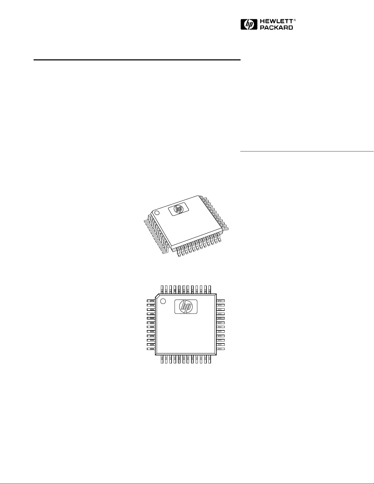
• TQFP-48 Surface Mount
Package
Plastic TQFP-48 Package
HPMX–5002
9433
019
6435
Pin Configuration
48
1
37
36
HPMX–5002
9433
6435 019
12
13
25
24
Description
The Hewlett-Packard HPMX-5002
IF Modulator/Demodulator
provides all of the active components necessary for the demodulation of a downconverted DECT
signal. Designed specifically for
DECT, the HPMX-5002 contains a
down-conversion mixer (to a 2nd
IF), limiting amplifier chain,
discriminator/data slicer, lock
detector, and RSSI circuits. The
LO2 generation is also included
on-chip, via a VCO, dividers, and
phase/frequency detector. The
divide ratios are programmable to
support reference frequencies of
either 9, 12, or 16 times the DECT
bit rate of 1.152␣ MHz allowing the
use of common, low cost crystals.
The LO2 VCO can also be utilized in
transmit mode by directly modulating the external VCO tank. An AGC
loop in the buffered VCO output
suppresses harmonics and reduces
signal level variability.
Applications
• DECT, Unlicensed PCS and
ISM Band Handsets,
Basestations and Wireless
LANs
7-105
The HPMX-5002 is designed to meet
the size and power demands of
portable applications. Battery cell
count and cost are reduced due to
the 2.7 V minimum supply voltage.
The TQFP-48 package, combined
with the high level of integration,
means smaller footprints and fewer
components. Flexible chip biasing
takes full advantage of the power
savings inherent in time-duplexed
systems such as DECT.
5965-9106E
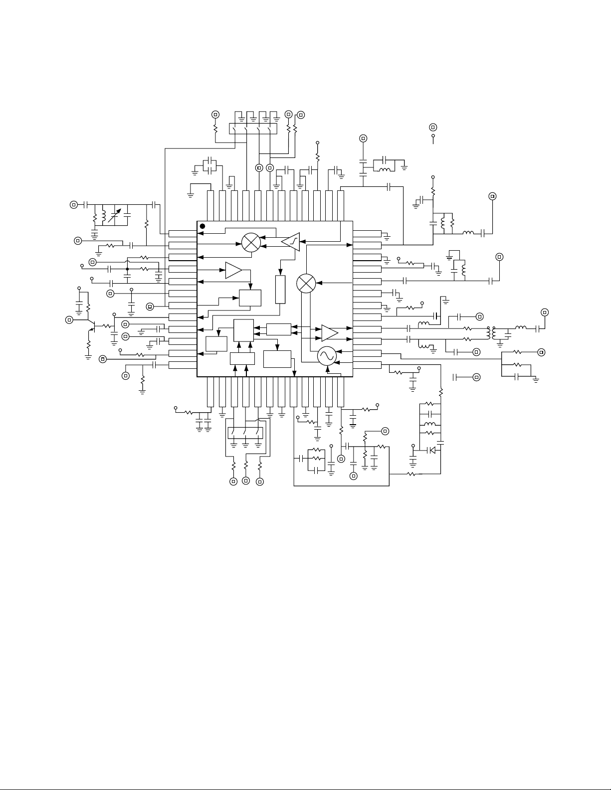
0.01 µ
6 kΩ
1000 p
0.01 µ
1 kΩ
15 µH
0.01 µ
0.01 µ
1 kΩ
3 to 10 p
49.9 Ω
68 p
0.01 µ
0 Ω
1000 p
22 p
0.01 µ
20 kΩ
4.7 kΩ
4.7 kΩ
49.9 Ω
3.9 p
0 Ω
10 p
22 p
1000 p
NC
LOCK
DET
BGR
4321
5
6
7 8
RX
NC
PLL
XLO
DATA
SLICER
φ
Freq.
Det.
9/12/16
90/216
CHARGE
PUMP
0.01 µ
R
S
S
I
100 kΩ
VSUB
100 kΩ
0.1 µ
0.01 µ
48 37
1
IFOP1
DMOD
DMODOP
BUF1
BUF2
TCNT
TCSET
DATOP
RSS1
LKFIL
LKDET
REF
12
NC
4
3
D1V3
NC
10 Ω
0.01 µ
VCC3
1000 p
VEE3
6
1
D1V1
5
2
D1V2
100 kΩ
10 Ω
0.01 µ 0.01 µ
VEE2
VCC2
DC1B
PFD
VEE4
VCC4
10 Ω
4.7 kΩ
3.3 kΩ
4400 p
330 p
0.01 µ
DC1A
AGC
1000 p
0.01 µ
100 p
0.01 µ
1F1P1
2413
VCOA
0 Ω
1000 p
0.01 µ
36
NC
IF1
VEE1
VCC1
IP1
IPDC
VEE5
VCC5
OSCOPB
OSCOP
VCOADJ
VCOB
25
1 kΩ
0.01 µ
1 kΩ
1 kΩ
10 p
2.7 µH
100 p
0 Ω
0.01 µ
0.01 µ
0.01 µ
0.01 µ
51.1 Ω
0.01 µ
0 Ω
10 p
10 Ω
270 nH
10 kΩ
0.01 µ
1 p
0.01 µ
270 nH
0.01 µ
= connector
= terminal
DC post
0 Ω
3.9 µH
0.01 µ
0 Ω
1 p
8.2 p
0.01 µ
0 Ω
3.9 p
120 n
10 kΩ
22 p
1.2 k Ω
8.2 p
3.9 µH
100 nH
0 Ω
0 Ω
68 p
22 p
220 nH
8.2 p
20 kΩ
20 kΩ
0.01 µ
1000 p
Figure 1. HPMX-5002 Test Board Schematic Diagram.
7-106
HPMX-5002 Functional Block Diagram
IFIP1
IF1
IFOP1
DMOD
DMODOP
BUF1
BUF2 TCSET
BIAS
RX
[1]
DATA
SLICER
9/12/16
DATAOP
RSSI
DIV2
DIV1
REF
BGR
Thermal Resistance
[2]
:
θjc = 80°C/W
Notes:
1. Operation of this device in excess
of any of these parameters may
cause permanent damage.
case
= 25°C
case
> 90°C
2. T
3. Derate at 10 mW/° C for T
IP1
RSSI
OSCOP
OSCOPB
90/216
CHARGE
PUMP
VCOBVCOADJ PLL XLO
DIV3VCOA
φ
FREQ.
DET.
LOCK
DET.
LKDETPFD
CONTROL
HPMX-5002 Absolute Maximum Ratings
Symbol Parameter Units Min. Max.
VCC Supply Voltage V -0.2 7.5
[4]
[2,3]
V -0.2 VCC + 0.2
m W 200
P
T
diss
STG
Voltage at any Pin
Power Dissipation
Junction Temperature °C +110
Storage Temperature °C -5 5 +125
4. Except CMOS logic inputs, see
Summary Characterization
Information Table.
HPMX-5002 Guaranteed Electrical Specifications
Unless otherwise noted, all parameters are guaranteed under the following conditions: 2.7 V < VCC < 5.5 V.
Test results are based upon use of networks shown in test diagram (see Figure 1). fin = 110.592 MHz.
Typical values are for V
Symbol Parameters and Test Conditions Units Min. Typ. Max.
I
ccx
Total V
(PLL locked)
(PLL locked) PLL mode mA 16 20
Charge pump current high current mode µA 400 550 1000
Charge pump current low current mode µA 30 50 100
GIF1 Mixer power gain from input matched to 50 Ω dB 5 8
IP1 to IF1, external load
impedance of 600 Ω
VDATOP Data slicer output level Logic ‘0’ V 0.3
VDATOP Data slicer output level Logic ‘1’ V V
= 3.0 V, TA = 25° C.
CCX
supply current RX mode mA 21 27
ccx
TX “flywheel” mode mA 9 11.5
Standby mode µA 100
- 0.3
ccx
7-107

HPMX-5002 Summary Characterization Information
Typical values measured on test board shown in Figure 1 at V
fin = 110.592 MHz, f
= 103.68 MHz, unless otherwise noted.
LO2
Symbol Parameters and Test Conditions Units Typ.
V
V
I
IH
IILCMOS input low current µA > - 50
P
1 dB
I
IP3
NF
Z
inIP1
Z
outRSSI
IF2f
A
VIF2
Z
inIFIP1
V
outLO2
ILKDET Lock detector current sink Logic ‘0’ (unlocked) mA 1.1
Notes:
1: RSSI signal is monotonic over stated dynamic range, but not necessarily linear. Voltage change is
defined in the linear region of the transfer curve.
2: IF2 frequency in the range 1 MHz < f < 45 MHz, with 10 nF capacitors from DC1A and DC1B to
ground.
CMOS input high voltage (can be pulled up as high as Vcc+7V) V ≥ Vcc-0.8
IH
CMOS input low voltage V ≤ 1.0
IL
CMOS input high current µA< 50
Mode switching time µS< 1
Mixer input 1 dB compression point matched to 50 Ω source dBm -23
Mixer input IP3 matched to 50 Ω source dBm -17
Mixer SSB noise figure input matched to 50 Ω dB 12
IF1
(see test diagram Fig. 1) source, 600 Ω load at output
Mixer input impedance 50 MHz < fin < 250 MHz Ω 100
RSSI dynamic range Note 1 dB 75
(for signal input at IFIP1; RSSI output measured with 6 bit ADC)
RSSI voltage change Note 1 mV/dB 17
RSSI output voltage. V
is monotonic - 90 dBm V 0.88
V
RSSI
= 3 V, 2 IF limiter input level:
ccx
RSSI output impedance kΩ 30
IF2 limiter bandwidth MHz 45
3 dB
IF2 limiter voltage gain Prior to limiting, Note 2 dB 57
IF2 limiter input impedance at pin IFIP1 Note 2 Ω 600
LO2 output buffer differential amplitude >1.5 kΩ differential load, mVp-p 335
(between OSCOP and OSCOPB) f
= 103.68 MHz, VCC=3 V
vco
Bit slicer time constant ratio TCSET =0 vs. TCSET = 1 80:1
LO2 VCO output buffer noise floor tank circuit Q =35 dBc/Hz -142
(@ 4 MHz offset)
PLL charge pump leakage current pA <100
= 3.0 V, TA = 25° C,
ccx
-50 dBm 1.48
-20 dBm 2.04
7-108

HPMX-5002 Pin Description
No. Mnemonic I/O Type Description
1 IFOP1 Analog O/P Output of IF amplifier, feeds quadrature network for discriminator
2 DMOD Analog I/P Input to discriminator mixer, driven by output of quadrature network
3 DMODOP Analog O/P Output of discriminator mixer, drives external low-pass data filter
4 BUF1 Analog I/P Noninverting input of buffer amplifier that drives the data slicer
5 BUF2 Analog O/P Output of buffer amplifer that drives the data slicer
6 TCNT Analog DC External capacitor connection which sets time constant for data slicer
7 TCSET CMOS I/P Data slicer time constant select
8 DATOP CMOS O/P Output bit stream from data slicer
9 RSSI Analog O/P Receive Signal Strength Indicator output
10 LKFIL Analog DC
11 LKDET CMOS O/P Indicates that LO2 PLL is in lock status
12 REF Analog I/P Reference signal for LO2 PLL
13 VCC3 DC Supply PLL supply voltage
14 VEE3 Ground PLL ground
15 DIV1 CMOS I/P Controls divide ratio for reference frequency input to the LO2 PLL
16 DIV2 CMOS I/P Controls divide ratio for reference frequency input to the LO2 PLL
17 DIV3 CMOS I/P Controls divide ratio for VCO frequency input to the LO2 PLL
20 PFD Analog O/P LO2 PLL phase/frequency detector charge pump output
21 VEE4 Ground LO2 VCO ground
22 VCC4 DC Supply LO2 VCO supply voltage
23 AGC Analog DC External capacitor connection to compensate LO2 VCO AGC loop
24 VCOA Analog I/P VCO tank force line
25 VCOB Analog O/P VCO tank sense line
26 VCOADJ Analog I/P Controls amplitude of buffered LO2 VCO output
27 OSCOP Analog O/P Buffered LO2 output (+)
28 OSCOPB Analog O/P Buffered LO2 output (-)
29 VCC5 DC Supply 1st IF supply voltage
30 VEE5 Ground 1st IF ground
31 IPDC Analog DC External capacitor connection for decoupling 1st IF bias point
32 IP1 Analog I/P 1st IF input signal
33 VCC1 DC Supply IF limiting amplifier supply voltage
34 VEE1 Ground IF limiting amplifier ground
35 IF1 Analog O/P Downconverted signal from front-end mixer, drives external filter
37 IFIP1 Analog I/P Input to IF limiting amplifier, driven by external filter
38 DC1A Analog DC External capacitor connection for decoupling IF limiting amplifier
39 VCC2 DC Supply IF limiting amplifier supply voltage
40 VEE2 Ground IF limiting amplifier ground
External capacitor connection which sets time constant for lock detector
(hi-Z output, open collector)
(600 Ω impedance, internally set)
7-109

HPMX-5002 Pin Description, continued
No. Mnemonic I/O Type Description
41 DC1B Analog DC External capacitor connection for decoupling IF limiting amplifier
42 VSUB Ground Substrate connection
43 XLO CMOS I/P
44 PLL CMOS I/P
45 RX CMOS I/P Controls bias to receive signal path, RSSI, data slicer
47 BGR Analog DC
18,19,
36, 46,
N/C Not All unconnected pins should be connected to a low-noise ground
connected
48
Controls bias to VCO and PLL components in conjunction with PLL pin
Controls bias to VCO and PLL components in conjunction with XLO pin
External capacitor connection for decoupling bandgap reference voltage
Table 1: HPMX-5002 Mode Control
(CMOS Logic Levels)
Mode PLL XLO RX
PLL 1 0 1
TX 0 0 1
RX 1 0 0
STBY 1 1 1
“flywheel” see text
Table 2: HPMX-5002 PLL Divider Programming
(CMOS Logic Levels)
REF divide by: DIV1 DIV2 DIV3
910X
12 0 0 X
16 0 1 X
Not defined 1 1 X
LO2 divide by:
90 X X 0
216 X X 1
7-110

IF1
IFIP1
IFOP1
DMOD
DMODOP
BUF1
BUF2 TCSET
IP1
OSCOP
OSCOPB
VCOBVCOADJ PLL XLO
Figure 2. HPMX-5002 Detailed Block Diagram.
Functional Description
Please refer to Figure 2, Detailed
Block Diagram, above. Figure 2
contains a graphical representation of all 32 active signal pins of
the HPMX-5002. For clarity, the
supply, ground, and substrate pins
are deleted.
90/216
CHARGE
PUMP
DIV3VCOA
Transmit mode (TX),
designed for use when the LO2
VCO is directly modulated by the
DECT data stream for subsequent
up-conversion to the channel
frequency (with the HPMX-5001
DECT Upconverter/Downconverter). In this mode, only the
VCO and LO2 output buffer are
Modes of Operation
The HPMX-5002 supports four
basic modes of operation. The logic
states necessary to program each
mode are listed in Table 1, Mode
Programming. The modes are:
biased and operational. In order
to use the LO2 VCO as a modulation source, it is necessary to first
program the HPMX-5002 in PLL
mode. Once the loop has achieved
lock, the PLL is then disabled by
setting the PLL pin to a logic 0.
Receive mode (RX),
which is used during the receive
time slot in DECT systems. All
blocks are powered on in this
mode.
This puts the VCO into “flywheel”
operation, preventing the PLL
from interfering with the modulation of the VCO. Leakage in the
tank circuit shown in Figure 3
allows the VCO to drift at a rate of
LO2 synthesis mode (PLL),
which enables the IC to achieve
2.5 kHz per mS, well within the
DECT specs of 13 kHz per mS.
phase lock without biasing the
receive signal path, thus saving
power. This is very useful for
DECT blind-slot applications.
φ
FREQ.
DET.
RSSI
LOCK
DET.
LKDETPFD
DATA
SLICER
9/12/16
BIAS
CONTROL
RX
Standby mode,
where all blocks are powered
down. This mode allows the
system designer to effectively turn
the IC off without having to use
battery control, and also allows
the IC to change quickly to an
active mode.
Detailed Circuit Description
PLL Section
The PLL section of the
HPMX-5002 contains three major
sections: a set of reference and
LO2 dividers, a phase/frequency
detector with charge pump, and a
lock detector.
The dividers for both the reference and LO2 signals in the PLL
section are programmable to
accomodate the most popular
DECT reference frequencies and
also to enable the use of higher
1st IF frequencies if desired.
DATAOP
RSSI
DIV2
DIV1
REF
BGR
7-111

Figure␣ 3 illustrates the logic states
necessary to program both the
reference and LO2 dividers.
The reference divider ratios were
selected to conform to the three
most popular DECT reference
frequencies of 10.368 MHz,
13.824␣ MHz, and 18.432 MHz. The
LO2 divider values allow the use
of either a 110.592 MHz or
112.32␣ MHz 1st IF with a divide
value of 90 (which yields a LO2 of
103.68 MHz). In addition, the
divide by 216 value permits the
use of a much higher 1st IF
(222.91␣ MHz, with a corresponding LO2 of 248.832 MHz), which
enables the use of much smaller
SAW filters and relaxes the image
filtering requirements.
The phase/frequency detector also
incorporates a lock detection
feature. The user must supply a
decoupling capacitor (recommended value of 1 nF) from the
LKFIL pin to ground. If the loop is
not in phase lock, the LKDET pin
will sink up to 1 mA. This open
collector output is utilized so that
this signal can be wire-ORed with
other lock detection circuits, such
as from the 1LO portion of the
system. The pullup resistor can
also be tied to the CMOS positive
supply, thus eliminating potential
problems with CMOS logic high
voltages when different positive
supplies are used between the
radio and the baseband processor.
When the PLL loop phase error is
less than approximately 0.3␣ radians, the LKDET current sink goes
to zero.
VCO Section
The VCO section has two major
components, a sustaining amplifier and a buffered external
output. The sustaining amplifer is
designed to be used with an
external tank circuit, and incorporates a force (VCOA) and sense
(VCOB) architecture to reduce the
effects of package parasitics. As
described earlier, the VCOB pin
may be overdriven by an external
LO, in which case the on-chip
sustaining amplifier acts as a
buffer stage before the
downconverting mixer.
The buffered external output is a
differential signal (OSCOP,
OSCOPB). The buffer also
incorporates an AGC loop in order
to provide a sinusoidal output
signal with constant amplitude
which is insensitive to variations
in tank Q and loading. This helps
to suppress harmonics and
eliminates therefore the need for
an upconversion filter if the
HPMX-5002 is used in a system
together with the 2.5 GHz
upconverter/downconverter
HPMX-5001. The AGC requires an
external compensation capacitor
(recommended value 1 nF) from
the AGC pin to ground.
Signal Path
The input to the HPMX-5002 is an
AC-coupled IF signal (IP1). The
input buffer before the
downconverting mixer requires a
decoupling capacitor from the
IPDC pin to ground (recommended value 10 pF).
The buffered input is then mixed
with the LO2, and the output of
the mixer (IF1) drives an off-chip
bandpass filter centered at the IF2
frequency (6.9 MHz for a 110.592
MHz 1IF). The filtered signal is
then fed to the IFIP1 pin, which is
the input to the limiting amplifier
chain. The limiting amplifier
requires two external decoupling
capacitors from pins DC1A and
DC1B to ground (recommended
value 10 nF).
The limiting amplifier chain also
feeds the Received Signal Strength
Indicator (RSSI) block. The RSSI
signal is monotonic over a 75 dB
dynamic range, and in its linear
range varies at 17 mV/dB. The
RSSI signal is designed to be
digitized by the CMOS burst mode
controller.
The output of the limiting amplifier (IFOP1) drives the discriminator circuit. This signal is fed
directly to one of the input ports
of a Gilbert cell mixer, and it also
drives an external quadrature
network (with a recommended Q
of 8 for optimum performance).
The output of the external quadrature network is then fed into the
other input port of the Gilbert cell
(via the DMOD pin). The output
of the Gilbert cell is taken at the
DMODOP pin, which drives an
external lowpass filter. To aid in
the construction of the filter, a
buffer stage is included on-chip.
The BUF1 pin is the noninverting
input of the buffer, and BUF2 is
the output, which is also connected to the input of the data
slicer.
The data slicer operates on a dual
time constant architecture,
controlled via the TCSET pin.
During the preamble portion of a
DECT timeslot (with TCSET set to
1), the data slicer quickly acquires
the midpoint voltage of the
incoming data stream, correcting
any DC offsets that may have
occurred due to frequency deviations within the DECT specification. The value of this initial time
constant is determined by an
external capacitor connected
between TCNT and ground. A
10␣ nF capacitor allows the accurate acquisition of the midpoint
voltage within half of the 16-bit
DECT preamble.
7-112

Once the midpoint voltage has
been acquired, TCSET is then
forced to a 0, and the time constant of the midpoint voltage
tracking circuit is increased by a
factor of 80. This effectively
freezes the midpoint voltage from
any variations due to normal data
transitions, but still allows for
some correction of frequency
drifts during the data burst.
The output of the data slicer
(DATOP) is a CMOS-compatible
bitstream. However, it is recommended that an external NPN
amplifier stage be used to drive
the CMOS baseband processor, in
order to minimize the amount of
ground and supply currents in the
HPMX-5002 which might desensitize the chip.
D: 1897.344 MHz
B: 1881.792 MHz
FRONT-END
RF FILTER
TX PA
T/R
RX LNA
CERAMIC
TX FILTER
CERAMIC
IMAGE
FILTER
HPMX-5001
IF1 = 110.592 MHz
SAW Channel Filter
LO2 = 103.68 MHz
X2
32/33
IF2 = 6.912 MHz
LC Filter
÷9
Charge
Pump
Tank
LC filter
Quad.
Network
φ
Freq.
Det.
RC filter
0: 893.376 MHz Rx
896.832 MHz Tx
9: 885.600 MHz Rx
889.056 MHz Tx
Tank
Freq.
÷N ÷12
SYNTHESIZER
N=1034 -1025 INCL. /32,33 Rx
N=1038 -1029 INCL. /32,33 Tx
PFD FREQ. = 864 kHz
Data
Filter
RSSI
Lock
HPMX-5002
Det.
PFD FREQ. = 1.152 MHz
Gaussian LPF
φ
Det.
Data
Slicer
÷9
TX Data
10.368 MHz
REFERENCE
OSCILLATOR
RX DATA
All other connections go to Burst Mode Controller, power source, or ground.
Figure 3. Typical HPMX-5002 Application with HPMX-5001 T/R Chip.
7-113

Circuit in the IC Small Signal Equivalent Circuit
(typical values)
Vcc
DMOD
Vcc
IFOP1
DMODOP
Pin 1
Pin 2
Pin 3
330 Ω
IFOP1
V
9 kΩ
DMOD
330 Ω
DMODOP
V
Vcc
BUF1
Vcc
BUF2
Figure 4. HPMX-5002 Internal and Equivalent Circuits, Pins 1-5.
Pin 4
Pin 5
7-114
>50 kΩ
BUF1
650 Ω
BUF2
V

Circuit in the IC
Vcc
Small Signal Equivalent Circuit
(typical values)
Vcc
Vcc
DATAOP
RSSI
RSSI
Pin 8
Pin 9
Pin 11
Vcc
RSSI
30 kΩ
Vcc
VCOA
VCOB
V
Pins 24, 25
Vcc
OSCOP
OSCOPS
Figure 5. HPMX-5002 Internal and Equivalent Circuits, Pins 8, 9, 11, 24, 25, 27, and 28.
Pins 27, 28
V
7-115
65 Ω
OSCOP
OSCOPB

Circuit in the IC Small Signal Equivalent Circuit
(typical values)
Vcc
IP1
IP1
Vcc
Vcc
Pin 32
IF1
100 Ω
Pin 35
V
IFIP1
IFIP1
Pin 37
Figure 6. HPMX-5002 Internal and Equivalent Circuits, Pins 32, 35, and 37.
7-116
600 Ω

Package Dimensions 48 Pin Thin Quad Flat Package
All dimensions shown in mm.
9.0±0.25
7.0±0.1
9.0±0.25
7.0±0.1
0.50.22 typ.
1.4±0.05
0.05 min., 0.1 max.
0.6+0.15, -0.10
Part Number Ordering Information
Part Number No. of Devices Container
HPMX-5002-STR 10 Strip
HPMX-5002-TR1 1000 Tape and Reel
HPMX-5002-TY1 250 Tray
7-117

Tape Dimensions and Product Orientation for Outline TQFP-48
REEL
CARRIER
TAPE
USER
FEED
DIRECTION
COVER TAPE
0.30 ± 0.05
2.0 (See Note 7)
4.0 (See Note 2)
1.5+0.1/-0.0 DIA
1.75
R 0.5 (2)
HPMX–5002
9433
5.0
1.6 (2)
B
O
K
1
K
O
6.4 (2)
A
O
6435 019
12.0
7.5 (See Note 7)
1.5 Min.
Cover tape width = 13.3 ± 0.1 mm
Cover tape thickness = 0.051 mm (0.002 inch)
NOTES:
AO = 9.3 mm
B
= 9.3 mm
O
K
= 2.2 mm
O
K
= 1.6 mm
1
1. Dimensions are in millimeters
2. 10 sprocket hole pitch cumulative tolerance ±0.2
3. Chamber not to exceed 1 mm in 100 mm
4. Material: black conductive Advantek™ polystyrene
5. A
and BO measured on a plane 0.3 mm above the bottom of the pocket.
O
6. K
measured from a plane on the inside bottom of the pocket to the top surface of the carrier.
O
7. Pocket position relative to sprocket hole measured as true position of pocket, not pocket hole.
16.0 ± 0.3
7-118
 Loading...