

1300 nm Fiber Optic
Transmitter and Receiver
Technical Data
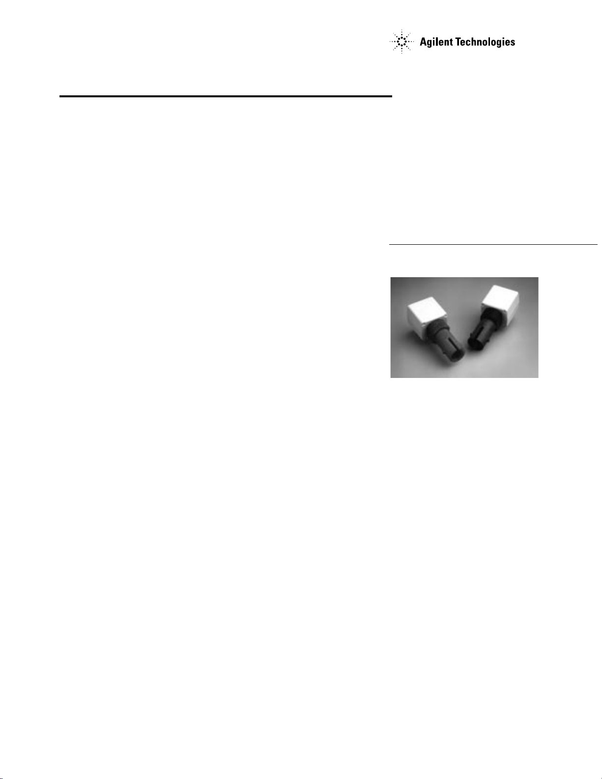
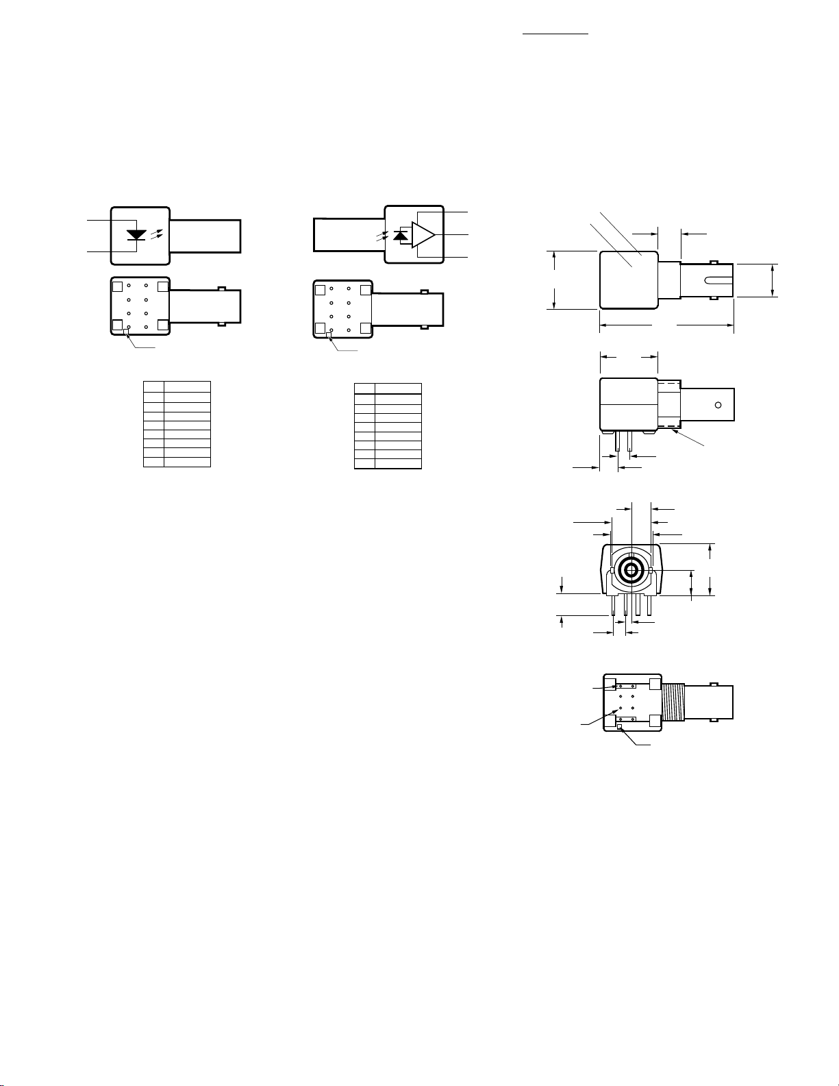
HFBR-1312T Transmitter
HFBR-2316T Receiver
Features
• Low Cost Fiber Optic Link
• Signal Rates over 155
Megabaud
• 1300 nm Wavelength
• Link Distances over 5 km
• Dual-in-line Package PanelMountable ST* and SC
Connector Receptacles
• Auto-Insertable and WaveSolderable
• Specified with 62.5/125 µm
and 50/125 µm Fiber
• Compatible with HFBR-0400
Series
• Receiver also Specified for
SM Cable Spec (9/125 µm)
Applications
• Desktop Links for High
Speed LANs
• Distance Extension Links
• Telecom Switch Systems
• TAXlchip® Compatible
Description
The HFBR-0300 Series is
designed to provide the most
cost-effective 1300 nm fiber optic
links for a wide variety of data
communication applications from
low-speed distance extenders up
to SONET OC-3 signal rates.
Pinouts identical to Agilent
HFBR-0400 Series allow
designers to easily upgrade their
820 nm links for farther distance.
The transmitter and receiver are
compatible with two popular
optical fiber sizes: 50/125 µm and
62.5/125 µm diameter. This
allows flexibility in choosing a
fiber size. The 1300 nm wavelength is in the lower dispersion
and attenuation region of fiber,
and provides longer distance
capabilities than 820 nm LED
technology. Typical distance
capabilities are 2 km at 125 MBd
and 5 km at 32 MBd.
Transmitter
The HFBR-1312T fiber optic
transmitter contains a 1300 nm
InGaAsP light emitting diode
capable of efficiently launching
optical power into 50/125 µm and
62.5/125 µm diameter fiber.
Converting the interface circuit
from a HFBR-14XX 820 nm
transmitter to the HFBR-1312T
requires only the removal of a few
passive components.
Receiver
The HFBR-2316T receiver contains an InGaAs PIN photodiode
and a low-noise transimpedance
preamplifier that operate in the
1300 nm wavelength region. The
HFBR-2316T receives an optical
signal and converts it to an analog
voltage. The buffered output is an
emitter-follower, with frequency
response from DC to typically 125
MHz. Low-cost external components can be used to convert the
analog output to logic compatible
signal levels for a variety of data
formats and data rates. The
*ST is a registered trademark of AT&T Lightguide Cable Connectors
2
HFBR-1312T Transmitter HFBR-2316T Receiver
2, 6
ANODE
3
CATHODE
5
4
6
3
7
2
8
1
BOTTOM VIEW
* PIN 7 IS ELECTRICALLY ISOLATED FROM
PINS 1, 4, 5, AND 8, BUT IS CONNECTED
TO THE HEADER.
† PINS 1, 4, 5, AND 8 ARE ISOLATED FROM
THE INTERNAL CIRCUITRY, BUT ARE
ELECTRICALLY CONNECTED TO EACH OTHER.
PIN NO. 1
INDICATOR
PINFUNCTION
1†
N.C.
2
ANODE
3
CATHODE
4†
N.C.
5†
N.C.
6
ANODE
7*
N.C.
8†
N.C.
BOTTOM VIEW
5
4
6
3
7
2
8
1
PIN NO. 1
INDICATOR
PINFUNCTION
1†
N.C.
2
SIGNAL
3*
V
EE
4†
N.C.
5†
N.C.
6
V
CC
7*
V
EE
8†
N.C.
* PINS 3 AND 7 ARE ELECTRICALLY
CONNECTED TO THE HEADER.
† PINS 1, 4, 5, AND 8 ARE ISOLATED FROM
THE INTERNAL CIRCUITRY, BUT ARE
ELECTRICALLY CONNECTED TO EACH OTHER.
6
2
3, 7
V
CC
ANALOG
SIGNAL
V
EE
HFBR-0300 Series
Mechanical Dimensions
PART NUMBER
DATE CODE
12.6
(0.495)
3.81
(0.150)
7.62
(0.300)
12.6
(0.495)
YYWW
HFBR-X31XT
29.8
(1.174)
2.54
(0.100)
6.30
(0.248)
(0.327)
5.05
(0.199)
3/8-32 UNEF-2A
8.31
7.05
(0.278)
DIA.
HFBR-2316T is pin compatible
with HFBR-24X6 receivers and
can be used to extend the
distance of an existing application
by substituting the HFBR-2316T
for the HFBR-2416.
Package Information
HFBR-0300 Series transmitters
and receivers are housed is a
dual-in-line package made of high
strength, heat resistant, chemically resistant, and UL V-0 flame
retardant plastic. Transmitters are
identified by the brown port
color; receivers have black ports.
The package is auto-insertable
and wave solderable for high
volume production applications.
Note: The “T” in the product
numbers indicates a Threaded ST
connector (panel mountable), for
both transmitter and receiver.
Handling and Design Information
When soldering, it is advisable to
leave the protective cap on the
unit to keep the optics clean.
Good system performance
requires clean port optics and
cable ferrules to avoid obstructing
the optical path. Clean compressed air is often sufficient to
remove particles of dirt; methanol
on a cotton swab also works well.
3.60
(0.140)
2.54
(0.100)
PINS 1,4,5,8
0.51 X 0.38
(0.020 X 0.015)
PINS 2,3,6,7
0.46
DIA
(0.018)
3
1
(0.050)
524
6
7
8
PIN NO. 1
INDICATOR
1.27
5.10
(0.202)
10.20
(0.400)
3
Panel Mounting Hardware
The HFBR-4411 kit consists of
100 nuts and 100 washers with
dimensions as shown in Figure 1.
These kits are available from
Agilent or any authorized distributor. Any standard size nut and
washer will work, provided the
total thickness of the wall, nut,
and washer does not exceed
0.2 inch (5.1mm).
3/8 - 32 UNEF -
2B THREAD
9.53
DIA.
(0.375)
12.70
DIA.
(0.50)
HEX-NUT
When preparing the chassis wall
for panel mounting, use the
mounting template in Figure 2.
When tightening the nut, torque
should not exceed 0.8 N-m
(8.0 in-lb).
Recommended Chemicals
for Cleaning/Degreasing
HFBR-0300 Products
Alcohols (methyl, isopropyl,
isobutyl)
1.65
(0.065)
14.27
(0.563)
TYP.
DIA.
9.80
(0.386)
DIA.
Aliphatics (hexane, heptane)
Other (soap solution, naphtha)
Do not use partially halogenated
hydrocarbons (such as 1.1.1 trichloroethane), ketones (such as
MEK), acetone, chloroform, ethyl
acetate, methylene dichloride,
phenol, methylene chloride, or Nmethylpyrolldone. Also, Agilent
does not recommend the use of
cleaners that use halogenated
hydrocarbons because of their
potential environmental harm.
10.41
MAX.
(0.410)
DIA.
INTERNAL TOOTH LOCK WASHER
ALL DIMENSIONS IN MILLIMETERS AND (INCHES).
Figure 1. HFBR-4411 Mechanical
Dimensions.
Figure 2. Recommended Cut-out for
Panel Mounting.
8.0
(0.315)
HFBR-1312T Transmitter Absolute Maximum Ratings
Parameter Symbol Min. Max. Unit Reference
Storage Temperature T
Operating Temperature T
S
A
Lead Soldering Cycle 260 °C
Temperature Note 8
Lead Soldering Cycle Time 10 sec
Forward Input Current DC I
Reverse Input Voltage V
CAUTION: The small junction sizes inherent to the design of this bipolar component increase the component's
susceptibility to damage from electrostatic discharge (ESD). It is advised that normal static precautions be
taken in handling and assembly of this component to prevent damage and/or degradation which may be
induced by ESD.
FDC
R
-55 85 °C
-40 85 °C
100 mA
1V

4
HFBR-1312T Transmitter Electrical/Optical Characteristics
0 to 70°C unless otherwise specified
Parameter Symbol Min. Typ.
Forward Voltage V
F
1.1 1.4 1.7 V IF = 75 mA Fig. 3
[1]
Max. Unit Condition Ref.
1.5 IF = 100 mA
Forward Voltage ∆VF/∆T -1.5 mV/°CIF = 75 - 100 mA
Temperature Coefficient
Reverse Input Voltage V
Center Emission λ
R
C
14 VI
= 100 µA
R
1270 1300 1370 nm
Wavelength
Full Width Half Maximum FWHM 130 185 nm
Diode Capacitance C
T
16 pF VF = 0 V, f = 1 MHz
Optical Power Temperature ∆PT/∆T -0.03 dB/°CIF = 75 - 100 mA DC
Coefficient
Thermal Resistance Θ
JA
260 °C/W Note 2
HFBR-1312T Transmitter Output Optical Power and Dynamic Characteristics
Condition
Parameter Symbol Min. Typ.
Peak Power P
62.5/125 µm
NA = 0.275
P
T62
T62
-16.0 -14.0 -12.5 dBm 25°C 75 mA Notes
-17.5 -11.5 0-70°C 75 mA
-15.5 -13.5 -12.0 25°C 100 mA
-17.0 -11.0 0-70°C 100 mA
Peak Power P
50/125 µm
NA = 0.20
P
T50
T50
-19.5 -17.0 -14.5 dBm 25°C 75 mA Notes
-21.0 -13.5 0-70°C 75 mA
-19.0 -16.5 -14.0 25°C 100 mA
-20.5 -13.0 0-70°C 100 mA
Optical Overshoot OS 5 10 % 0-70°C 75 mA Note 6
Rise Time t
Fall Time t
r
f
[1]
Max. Unit T
A
I
F, peak
3, 4, 5
Fig. 4
3, 4, 5
Fig. 4
Fig. 5
1.8 4.0 ns 0-70°C 75 mA Note 7
Fig. 5
2.2 4.0 ns 0-70°C 75 mA Note 7
Fig. 5
Ref.

5
Transmitter Notes:
1. Typical data are at TA = 25°C.
2. Thermal resistance is measured with the transmitter coupled to a connector assembly and mounted on a printed circuit board;
ΘJC < ΘJA.
3. Optical power is measured with a large area detector at the end of 1 meter of mode stripped cable, with an ST* precision ceramic
ferrule (MIL-STD-83522/13), which approximates a standard test connector. Average power measurements are made at 12.5 MHz
with a 50% duty cycle drive current of 0 to I
power.
4. When changing from µW to dBm, the optical power is referenced to 1 mW (1000 µW).
Optical power P(dBm) = 10*log[P(µW)/1000µW].
5. Fiber NA is measured at the end of 2 meters of mode stripped fiber using the far-field pattern. NA is defined as the sine of the half
angle, determined at 5% of the peak intensity point. When using other manufacturer’s fiber cable, results will vary due to differing
NA values and test methods.
6. Overshoot is measured as a percentage of the peak amplitude of the optical waveform to the 100% amplitude level. The 100%
amplitude level is determined at the end of a 40 ns pulse, 50% duty cycle. This will ensure that ringing and other noise sources have
been eliminated.
7. Optical rise and fall times are measured from 10% to 90% with 62.5/125 µm fiber. LED response time with recommended test
circuit (Figure 3) at 25 MHz, 50% duty cycle.
8. 2.0 mm from where leads enter case.
F,peak
; I
F,average
= I
/2. Peak optical power is 3 dB higher than average optical
F,peak
100
90
80
70
60
50
40
– FORWARD CURRENT – mA
F
I
30
20
1.1 1.2 1.3 1.4 1.5 1.6
V
– FORWARD VOLTAGE – V
F
Figure 3. Typical Forward Voltage and Current
Characteristics.
10 µF
TANTALUM
NE46134
2.7 Ω
DATA +
DATA –
0.1 µF
+ 5.0 V
1
16
53
MC10H116A
4
10
MC10H116B
9
11
V
bb
13
MC10H116C
12
8
75 Ω
2
75 Ω
7
6
15
14
220 Ω
NOTES:
1. ALL RESISTORS ARE 5% TOLERANCE.
2. BEST PERFORMANCE WITH SURFACE MOUNT COMPONENTS.
3. DIP MOTOROLA MC10H116 IS SHOWN, PLCC MAY ALSO BE USED.
1.2
1.1
1.0
0.9
0.8
0.7
0.6
0.5
RELATIVE POWER RATIO
0.4
0.3
0.2
10 30 50 70 90
IF – FORWARD CURRENT – mA
Figure 4. Normalized Transmitter Output Power vs.
Forward Current.
HFBR-1312T
24 Ω
150 Ω
NE46134
2.7 Ω
2, 6
3
7
220 Ω
0.1
µF
Figure 5. Recommended Transmitter Drive and Test Circuit.

6
HFBR-2316T Receiver Absolute Maximum Ratings
Parameter Symbol Min. Max. Unit Reference
Storage Temperature T
Operating Temperature T
S
A
Lead Soldering Temperature 260 °C Note 1
Cycle Time
Signal Pin Voltage V
Supply Voltage VCC - V
Output Current I
CAUTION: The small junction sizes inherent to the design of this bipolar component increase the component's
susceptibility to damage from electrostatic discharge (ESD). It is advised that normal static precautions be
taken in handling and assembly of this component to prevent damage and/or degradation which may be
induced by ESD.
O
EE
O
-55 85 °C
-40 +85 °C
10 s
-0.5 V
CC
V
-0.5 6.0 V Note 2
25 mA
HFBR-2316T Receiver Electrical/Optical and Dynamic Characteristics
0 to 70°C; 4.75 V < VCC - VEE < 5.25 V; power supply must be filtered (see note 2).
Parameter Symbol Min. Typ.
Responsitivity RP 62.5 µm 6.5 13 19 mV/µW λp = 1300 nm, 50 MHz Note 4
R
9 µm 8.5 17 Singlemode Fiber
P
RMS Output Noise V
NO
Voltage PR = 0 µ W Fig. 7
Equivalent Optical P
N, RMS
Noise Input Power
(RMS)
Peak Input Optical P
R
Power
Output Resistance R
DC Output Voltage V
Supply Current I
Electrical Bandwidth BW
O
O,DC
CC
0.8 1.8 2.6 V VCC = 5 V, VEE = 0 V
E
75 125 MHz -3 dB electrical Note 7
Bandwidth * Rise 0.41 Hz *s Note 11
Time Product
Electrical Rise, Fall tr,t
f
Times, 10-90% @ 50 MHz Fig. 9
Pulse-Width PWD 0.4 1.0 ns PR = -11 dBm, peak Note 6,9
Distortion Fig. 8
Overshoot 2 % PR = -15 dBm, peak Note 10
[3]
Max. Unit Condition Ref.
Multimode Fiber Fig. 6,
62.5/125 µm10
9/125µm
0.4 0.59 mV
1.0 mV
100 MHz Bandwidth, Note 5
RMS
Unfiltered Bandwidth
RMS
PR = 0 µW
-45 -41.5 dBm @ 100 MHz, PR = 0 µW Note 5
0.032 0.071 µW
-11.0 dBm 50 MHz, 1 ns PWD Note 6
80 µW
Fig. 8
30 Ohm f = 50 MHz
PR = 0 µ W
915mAR
LOAD
= ∞
3.3 5.3 ns PR = -15 dBm peak, Note 8

7
Receiver Notes:
1. 2.0 mm from where leads enter case.
2. The signal output is referred to VCC, and does not reject noise from the VCC power supply. Consequently, the VCC power supply must
be filtered. The recommended power supply is +5 V on VCC for typical usage with +5 V ECL logic. A -5 V power supply on VEE is
used for test purposes to minimize power supply noise.
3. Typical specifications are for operation at TA = 25°C and VCC = +5 VDC.
4. The test circuit layout should be in accordance with good high frequency circuit design techniques.
5. Measured with a 9-pole “brick wall” low-pass filter [Mini-CircuitsTM, BLP-100*] with -3 dB bandwidth of 100 MHz.
6. -11.0 dBm is the maximum peak input optical power for which pulse-width distortion is less than 1 ns.
7. Electrical bandwidth is the frequency where the responsivity is -3 dB (electrical) below the responsivity measured at 50 MHz.
8. The specifled rise and fall times are referenced to a fast square wave optical source. Rise and fall times measured using an LED
optical source with a 2.0 ns rise and fall time (such as the HFBR-1312T) will be approximately 0.6 ns longer than the specifled rise
and fall times. E.g.: measured t
~ [(specifled t
r,f
)2 + (test source optical t
r,f
9. 10 ns pulse width, 50% duty cycle, at the 50% amplitude point of the waveform.
10. Percent overshoot is defined as: ((VPK - V
100%
)/V
) x 100% . The overshoot is typically 2% with an input optical rise time ≤ 1.5 ns.
100%
11. The bandwidth*risetime product is typically 0.41 because the HFBR-2316T has a second-order bandwidth limiting characteristic.
V = 0 V
10 Ω
0.1 µF
CC
6
3, 7
V = -5 V
EE
V
O
2
TEST
LOAD
<
5 pF
–
500 Ω
500 Ω
100 pF
V = -5 V
EE
1 GHz FET PROBE
0.1 µF
HFBR-2316T
100 pF
1/2
)2]
.
r,f
150
Z
125
100
75
50
25
SPECTRAL NOISE DENSITY – nV/ H
0
0 50 100 150 200 250
FREQUENCY – MH
Z
300
Figure 6. HFBR-2316T Receiver Test Circuit.
3.0
2.5
2.0
1.5
1.0
0.5
PWD – PULSE WIDTH DISTORTION – ns
0
0 20 40 60 100
P
– INPUT OPTICAL POWER – µW
R
80
Figure 8. Typical Pulse Width
Distortion vs. Peak Input Power.
120
– RESPONSE TIME – ns
f
, t
r
t
Figure 9. Typical Rise and Fall Times
vs. Temperature.
*Mini-Circuits Division of Components Corporation.
6.0
5.0
4.0
3.0
2.0
1.0
t
f
t
r
-60 -40 -20 0 20 40
TEMPERATURE – °C
Figure 7. Typical Output Spectral
Noise Density vs. Frequency.
1.1
1.0
0.9
0.8
0.7
0.6
0.5
0.4
NORMALIZED RESPONSE
0.3
0.2
0.1
80 100
60
900 1000 1100 1200 1300 1400
λ – WAVELENGTH – nm
1500
1600 1700
Figure 10. Normalized Receiver
Spectral Response.

www.semiconductor.agilent.com
Data subject to change.
Copyright © 2001 Agilent Technologies, Inc.
June 6, 2001
Obsoletes 5965-3611E (11/99)
5988-2576EN
 Loading...