

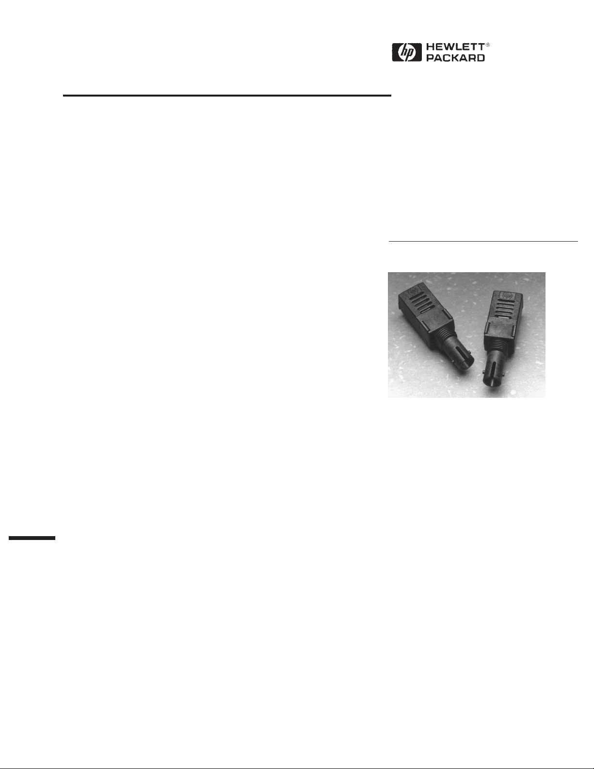
Fiber Optic Transmitter
and Receiver Data Links
for 125 MBd
Technical Data
HFBR-1115T Transmitter
HFBR-2115T Receiver
Features
• Full Compliance with the
Optical Performance
Requirements of the FDDI
PMD Standard
• Full Compliance with the
Optical Performance
Requirements of the ATM
100 Mbps Physical Layer
• Full Compliance with the
Optical Performance
Requirements of the
100 Mbps Fast Ethernet
Physical Layer
• Other Versions Available for:
- ATM
- Fibre Channel
• Compact 16-pin DIP Package
with Plastic ST* Connector
• Wave Solder and Aqueous
Wash Process Compatible
Package
• Manufactured in an ISO
9001 Certified Facility
Applications
• FDDI Concentrators,
Bridges, Routers, and
Network Interface Cards
• 100 Mbps ATM Interfaces
• Fast Ethernet Interfaces
• General Purpose, Point-toPoint Data Communications
• Replaces DLT/R1040-ST1
Model Transmitters and
Receivers
*ST is a registered trademark of AT&T Lightguide Cable Connectors.
5965-3481E (8/96)
Description
The HFBR-1115/-2115 series of
data links are high-performance,
cost-efficient, transmitter and
receiver modules for serial
optical data communication
applications specified at 100
Mbps for FDDI PMD or 100 BaseFX Fast Ethernet applications.
These modules are designed for
50 or 62.5 µm core multi-mode
optical fiber and operate at a
nominal wavelength of 1300 nm.
They incorporate our highperformance, reliable, longwavelength, optical devices and
proven circuit technology to give
long life and consistent
performance.
Transmitter
The transmitter utilizes a
1300 nm surface-emitting
InGaAsP LED, packaged in an
optical subassembly. The LED is
dc-coupled to a custom IC which
converts differential-input, PECL
logic signals, ECL-referenced
(shifted) to a +5 V power supply,
into an analog LED drive current.
Receiver
The receiver utilizes an InGaAs
PIN photodiode coupled to a
custom silicon transimpedance
preamplifier IC. The PINpreamplifier combination is accoupled to a custom quantizer IC
which provides the final pulse
shaping for the logic output and
the Signal Detect function. Both
the Data and Signal Detect
Outputs are differential. Also,
both Data and Signal Detect
Outputs are PECL compatible,
ECL-referenced (shifted) to a
+5 V power supply.
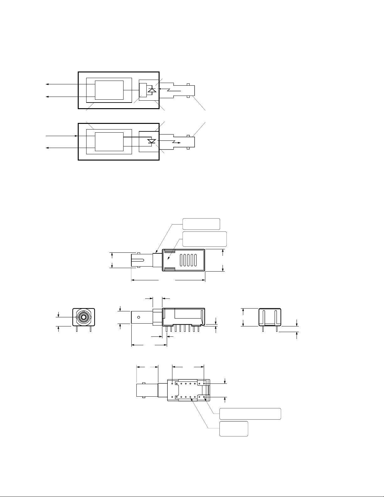
Package
The overall package concept for
the Data Links consists of the
following basic elements: two
optical subassemblies, two
electrical subassemblies, and the
outer housings as illustrated in
Figure 1.
177
DIFFERENTIAL
DATA IN
DIFFERENTIAL
SIGNAL
DETECT OUT
DIFFERENTIAL
DATA IN
V
BB
RECEIVER
QUANTIZER
IC
ELECTRICAL
SUBASSEMBLIES
TRANSMITTER
DRIVER IC
TOP VIEW
PREAMP IC
PIN PHOTODIODE
OPTICAL
SUBASSEMBLIES
LED
Figure 1. Transmitter and Receiver Block Diagram.
SIMPLEX ST
RECEPTACLE
THREADS
3/8 – 32 UNEF-2A
HFBR-111X/211XT
DATE CODE (YYWW)
SINGAPORE
The package outline drawing and
pinout are shown in Figures 2
and 3. The details of this package
outline and pinout are compatible
with other data-link modules from
®
other vendors.
8.31
5.0
NOTES:
1. MATERIAL ALLOY 194 1/2H – 0.38 THK
FINISH MATTE TIN PLATE 7.6 µm MIN.
2. MATERIAL PHOSPHOR BRONZE WITH
120 MICROINCHES TIN LEAD (90/10)
OVER 50 MICROINCHES NICKEL.
3. UNITS = mm
7.01
Figure 2. Package Outline Drawing.
5.05
2.45
19.72
12
41 MAX.
17.78
(7 x 2.54)
12.19
MAX.
0.9
9.8 MAX.
8 x 7.62
HOUSING PINS 0.38 x 0.5 mm
NOTE 1
PCB PINS
DIA. 0.46 mm
NOTE 2
3
178
NC
GND
V
CC
V
CC
GND
DATA
DATA
NC
OPTICAL PORT
9NC
8
10 NO PIN
7
11 GND
6
12 GND
5
13 GND
4
14 GND
3
15 V
2
BB
16 NC
1
NC
NO PIN
GND
GND
GND
SD
SD
NO PIN
OPTICAL PORT
9NC
8
10 GND
7
11 V
6
CC
12 V
5
CC
13 V
4
CC
14 DATA
3
15 DATA
2
16 NC
1
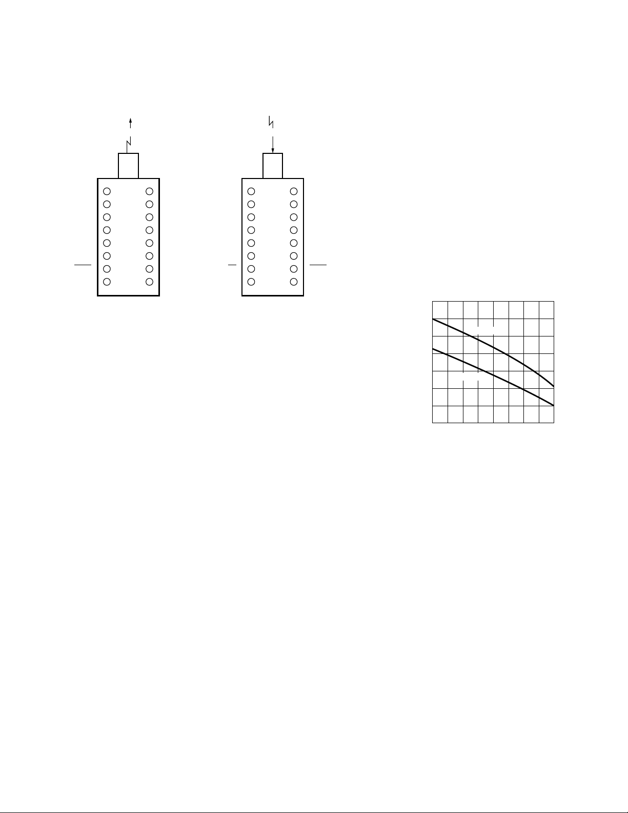
Figure 4 illustrates the predicted
OPB associated with the transmitter and receiver specified in this
data sheet at the Beginning of Life
(BOL). This curve represents the
attenuation and chromatic plus
modal dispersion losses associated
with 62.5/125 µm and 50/125 µm
fiber cables only. The area under
the curve represents the remaining
OPB at any link length, which is
available for overcoming non-fiber
cable related losses.
TRANSMITTER
Figure 3. Pinout Drawing.
The optical subassemblies consist
of a transmitter subassembly in
which the LED resides and a
receiver subassembly housing the
PIN-preamplifier combination.
The electrical subassemblies consist of a multi-layer printed circuit
board on which the IC chips and
various sufrace-mounted, passive
circuit elements are attached.
Each transmitter and receiver
package includes an internal shield
for the electrical subassembly to
ensure low EMI emissions and high
immunity to external EMI fields.
The outer housing, including the
ST* port, is molded of filled, nonconductive plastic to provide
mechanical strength and electrical
isolation. For other port styles,
please contact your HewlettPackard Sales Representative.
Each data-link module is attached
to a printed circuit board via the
16-pin DIP interface. Pins 8 and 9
provide mechanical strength for
these plastic-port devices and will
provide port-ground for forthcoming metal-port modules.
RECEIVER
Application Information
The Applications Engineering
group of the Optical Communication Division is available to assist
you with the technical understanding and design tradeoffs associated
with these transmitter and receiver
modules. You can contact them
through your Hewlett-Packard
sales representative.
The following information is
provided to answer some of the
most common questions about the
use of these parts.
Transmitter and Receiver Optical Power Budget versus Link Length
The Optical Power Budget (OPB)
is the available optical power for a
fiber-optic link to accommodate
fiber cable losses plus losses due to
in-line connectors, splices, optical
switches, and to provide margin for
link aging and unplanned losses
due to cable plant reconfiguration
or repair.
14
12
10
8
6
4
2
0
OPB – OPTICAL POWER BUDGET – dB
0 4.0
FIBER OPTIC CABLE LENGTH – km
Figure 4. Optical Power Budget at
BOL vs. Fiber Optic Cable Length.
62.5/125 µm
50/125 µm
0.5 1.5 2.0 2.5
1.0 3.0
3.5
Hewlett-Packard LED technology
has produced 1300 nm LED
devices with lower aging
characteristics than normally associated with these technologies in
the industry. The industry
convention is 1.5 dB aging for
1300 nm LEDs; however, HP 1300
nm LEDs will experience less than
1 dB of aging over normal
commercial equipment mission-life
periods. Contact your HewlettPackard sales representative for
additional details.
Figure 4 was generated with a
Hewlett-Packard fiber-optic link
model containing the current
industry conventions for fiber
179
cable specifications and the FDDI
PMD optical parameters. These
parameters are reflected in the
guaranteed performance of the
transmitter and receiver specifications in this data sheet. This same
model has been used extensively in
the ANSI and IEEE committees,
including the ANSI X3T9.5
committee, to establish the optical
performance requirements for
various fiber-optic interface
standards. The cable parameters
used come from the ISO/IEC JTC1/
SC 25/WG3 Generic Cabling for
Customer Premises per DIS 11801
document and the EIA/TIA-568-A
Commercial Building Telecommunications Cabling Standard per
SP-2840.
Transmitter and Receiver Signaling Rate Range and BER Performance
For purposes of definition, the
symbol rate (Baud), also called
signaling rate, is the reciprocal of
the symbol time. Data rate (bits/
sec) is the symbol rate divided by
the encoding factor used to encode
the data (symbols/bit).
When used in FDDI, ATM 100
Mbps, and Fast Ethernet
applications, the performance of
Hewlett-Packard’s 1300 nm HFBR1115/-2115 data link modules is
guaranteed over the signaling rate
of 10 MBd to 125 MBd to the full
conditions listed in the individual
product specification tables.
The data link modules can be used
for other applications at signaling
rates outside of the 10 MBd to 125
MBd range with some penalty in
the link optical power budget
primarily caused by a reduction of
receiver sensitivity. Figure 5 gives
an indication of the typical
performance of these 1300 nm
products at different rates.
3.0
2.5
2.0
1.5
1.0
0.5
0
POWER BUDGET AT CONSTANT BER (dB)
TRANSMITTER/RECEIVER RELATIVE OPTICAL
CONDITIONS:
1. PRBS 2
2. DATA SAMPLED AT CENTER OF DATA SYMBOL.
3. BER = 10
4. TA = 25° C
= 5 Vdc
5. V
CC
6. INPUT OPTICAL RISE/FALL TIMES = 1.0/2.1 ns.
Figure 5. Transmitter/Receiver
Relative Optical Power Budget at
Constant BER vs. Signaling Rate.
50 150
0 200
25 75 100 125
SIGNAL RATE (MBd)
7
-1
-6
175
These data link modules can also
be used for applications which
require different bit-error-ratio
(BER) performance. Figure 6
illustrates the typical trade-off
between link BER and the receiver
input optical power level.
-2
1 x 10
-3
1 x 10
-4
1 x 10
-5
1 x 10
-6
1 x 10
-7
1 x 10
-8
1 x 10
BIT ERROR RATIO
-10
2.5 x 10
-11
1 x 10
-12
1 x 10
-6 4
RELATIVE INPUT OPTICAL POWER – dB
CONDITIONS:
1. 125 MBd
2. PRBS 2
= 25° C
3. T
A
= 5 Vdc
4. V
CC
5. INPUT OPTICAL RISE/FALL TIMES = 1.0/2.1 ns.
Figure 6. Bit-Error-Ratio vs. Relative
Receiver Input Optical Power.
-4 2-2
7
-1
CENTER OF
SYMBOL
0
Data Link Jitter Performance
The Hewlett-Packard 1300 nm data
link modules are designed to
operate per the system jitter
allocations stated in Table E1 of
Annex E of the FDDI PMD
standard.
The 1300 nm transmitter will
tolerate the worst-case input
electrical jitter allowed in the table
without violating the worst-case
output jitter requirements of
Section 8.1 Active Output Interface
of the FDDI PMD standard.
The 1300 nm receiver will tolerate
the worst-case input optical jitter
allowed in Section 8.2 Active Input
Interface of the FDDI PMD
standard without violating the
worst-case output electrical jitter
allowed in the Table E1 of the
Annex E.
The jitter specifications stated in
the following transmitter and
receiver specification table are
derived from the values in Table
E1 of Annex E. They represent the
worst-case jitter contribution that
the transmitter and receiver are
allowed to make to the overall
system jitter without violating the
Annex E allocation example. In
practice, the typical jitter
contribution of the HewlettPackard data link modules is well
below the maximum amounts.
Recommended Handling Precautions
It is advised that normal static
precautions be taken in the
handling and assembly of these
data link modules to prevent
damage which may be induced by
electrostatic discharge (ESD). The
HFBR-1115/-2115 series meets
MIL-STD-883C Method 3015.4
Class 2.
180

Care should be taken to avoid
shorting the receiver Data or
Signal Detect Outputs directly to
ground without proper currentlimiting impedance.
Solder and Wash Process Compatibility
The transmitter and receiver are
delivered with protective process
caps covering the individual ST*
ports. These process caps protect
the optical subassemblies during
wave solder and aqueous wash
processing and act as dust covers
during shipping.
These data link modules are
compatible with either industry
standard wave- or hand-solder
processes.
Shipping Container
The data link modules are
packaged in a shipping container
designed to protect it from
mechanical and ESD damage
during shipment or storage.
Board Layout–Interface Circuit and Layout Guidelines
It is important to take care in the
layout of your circuit board to
achieve optimum performance
from these data link modules.
Figure 7 provides a good example
of a power supply filter circuit that
works well with these parts. Also,
suggested signal terminations for
the Data, Data-bar, Signal Detect
and Signal Detect-bar lines are
shown. Use of a multilayer,
ground-plane printed circuit board
will provide good high-frequency
9 NC
NO
10
PIN
11 GND
12 GND
13 GND
14 SD
15 SD
NO
16
PIN
Rx
CC
CC
CC
D 3
D
NC 1
*
6
C6
0.1
C1
0.1
R10
130
5
4
2
L1
1
C7
10
(OPTIONAL)
R9
82
R11
82
R12
130
TERMINATE D, D, SD, SD AT
INPUTS OF FOLLOW-ON DEVICES
C3
0.1C410
R8
R5
R7
82
130
82
) TO GROUND WITHOUT
BB
NC 8
GND 7
V
V
V
Tx
*
R1
130
9 NC
10 GND
11 V
12 V
13 GND
14 D
15 D
16 NC
A
+5 Vdc
GND
DATA
DATA
NOTES:
1. RESISTANCE IS IN OHMS. CAPACITANCE IS IN MICROFARADS. INDUCTANCE IS IN MICROHENRIES.
2. TERMINATE TRANSMITTER INPUT DATA AND DATA-BAR AT THE TRANSMITTER INPUT PINS. TERMINATE THE RECEIVER OUTPUT DATA, DATA-BAR, AND SIGNAL DETECTBAR AT THE FOLLOW-ON DEVICE INPUT PINS. FOR LOWER POWER DISSIPATION IN THE SIGNAL DETECT TERMINATION CIRCUITRY WITH SMALL COMPROMISE TO THE
SIGNAL QUALITY, EACH SIGNAL DETECT OUTPUT CAN BE LOADED WITH 510 OHMS TO GROUND INSTEAD OF THE TWO RESISTOR, SPLIT-LOAD PECL TERMINATION
SHOWN IN THIS SCHEMATIC.
3. MAKE DIFFERENTIAL SIGNAL PATHS SHORT AND OF SAME LENGTH WITH EQUAL TERMINATION IMPEDANCE.
4. SIGNAL TRACES SHOULD BE 50 OHMS MICROSTRIP OR STRIPLINE TRANSMISSION LINES. USE MULTILAYER, GROUND-PLANE PRINTED CIRCUIT BOARD FOR BEST HIGHFREQUENCY PERFORMANCE.
5. USE HIGH-FREQUENCY, MONOLITHIC CERAMIC BYPASS CAPACITORS AND LOW SERIES DC RESISTANCE INDUCTORS. RECOMMEND USE OF SURFACE-MOUNT COIL
INDUCTORS AND CAPACITORS. IN LOW NOISE POWER SUPPLY SYSTEMS, FERRITE BEAD INDUCTORS CAN BE SUBSTITUTED FOR COIL INDUCTORS. LOCATE POWER
SUPPLY FILTER COMPONENTS CLOSE TO THEIR RESPECTIVE POWER SUPPLY PINS. C7 IS AN OPTIONAL BYPASS CAPACITOR FOR IMPROVED, LOW-FREQUENCY NOISE
POWER SUPPLY FILTER PERFORMANCE.
6. DEVICE GROUND PINS SHOULD BE DIRECTLY AND INDIVIDUALLY CONNECTED TO GROUND.
7. CAUTION: DO NOT DIRECTLY CONNECT THE FIBER-OPTIC MODULE PECL OUTPUTS (DATA, DATA-BAR, SIGNAL DETECT, SIGNAL DETECT-BAR, V
PROPER CURRENT LIMITING IMPEDANCE.
8. (*) OPTIONAL METAL ST OPTICAL PORT TRANSMITTER AND RECEIVER MODULES WILL HAVE PINS 8 AND 9 ELECTRICALLY CONNECTED TO THE METAL PORT ONLY AND
NOT CONNECTED TO THE INTERNAL SIGNAL GROUND.
R3
R2
82
82
C5
0.1
TERMINATE D, D
AT Tx INPUTS
L2
1
C2
0.1
R4
130
CC
CC
NC 8
PIN
GND 6
GND 5
GND 4
GND 3
V
NO
BB
NC 1
*
7
2
*
TOP VIEWS
SD
130
A
DATA
DATA
R6
SD
Figure 7. Recommended Interface Circuitry and Power Supply Filter Circuits.
181

circuit performance with a low
inductance ground return path. See
additional recommendations noted
in the interface schematic shown in
Figure 7.
Board Layout–Hole Pattern
The Hewlett-Packard transmitter
and receiver hole pattern is
compatible with other data link
modules from other vendors. The
drawing shown in Figure 8 can be
used as a guide in the mechanical
layout of your circuit board.
Regulatory Compliance
These data link modules are
intended to enable commercial
system designers to develop
equipment that complies with the
various international regulations
governing certification of Information Technology Equipment.
Additional information is available
from your Hewlett-Packard sales
representative.
All HFBR-1115T LED transmitters
are classified as IEC-825-1
Accessible Emission Limit (AEL)
Class 1 based upon the current
proposed draft scheduled to go
0.8 ± 0.1
ø
(16X)
.032 ± .004
Ø 0.000
MA
–A–
into effect on January 1, 1997. AEL
Class 1 LED devices are considered eye safe. See Application Note
1094, LED Device Classifications
with Respect to AEL Values as
Defined in the IEC 825-1
Standard and the European
EN60825-1 Directive.
The material used for the housing
in the HFBR-1115/-2115 series is
Ultem 2100 (GE). Ultem 2100 is
recognized for a UL flammability
rating of 94V-0 (UL File Number
E121562) and the CSA (Canadian
Standards Association) equivalent
(File Number LS88480).
17.78
.700
(7X)
7.62
.300
Figure 8. Recommended Board Layout Hole Pattern.
TOP VIEW
182
2.54
.100
UNITS = mm/INCH

200
180
1.5
160
2.0
140
2.5
3.0
120
3.5
SPECTRAL WIDTH (FWHM) –nm
100
∆λ – TRANSMITTER OUTPUT OPTICAL
1280 1300 1320
λC – TRANSMITTER OUTPUT OPTICAL
CENTER WAVELENGTH –nm
HFBR-1115T FDDI TRANSMITTER TEST RESULTS
, ∆λ AND t
OF λ
C
COMPLY WITH THE ALLOWED SPECTRAL WIDTH
AS A FUNCTION OF CENTER WAVELENGTH FOR
VARIOUS RISE AND FALL TIMES.
t
– TRANSMITTER
r/f
OUTPUT OPTICAL
RISE/FALL TIMES – ns
ARE CORRELATED AND
r/f
3.0
3.5
1380
13601340
Figure 9. HFBR-1115T Transmitter
Output Optical Spectral Width
(FWHM) vs. Transmitter Output
Optical Center Wavelength and Rise/
Fall Times.
4.40
1.25
1.025
1.00
0.975
0.90
0.50
RELATIVE AMPLITUDE
0% TIME
INTERVAL
0.10
0.025
0.0
-0.025
-0.05
10.0
THE HFBR-1115T OUTPUT OPTICAL PULSE SHAPE FITS WITHIN THE BOUNDARIES
OF THE PULSE ENVELOPE FOR RISE AND FALL TIME MEASUREMENTS.
1.975
5.6
0.075
100% TIME
INTERVAL
± 0.725
1.525
0.525
4.850
80 ± 500 ppm
TIME – ns
40 ± 0.7
10.0
± 0.725
0.075
1.975
5.6
4.40
4.850
1.525
0.525
5
4
3
2
1
0
RELATIVE INPUT OPTICAL POWER – dB
-4 4
-3 -1 0 1
EYE SAMPLING TIME POSITION (ns)
CONDITIONS:
= 25° C
1.T
A
= 5 Vdc
2. V
CC
3. INPUT OPTICAL RISE/FALL TIMES = 1.0/2.1 ns.
4. INPUT OPTICAL POWER IS NORMALIZED TO
CENTER OF DATA SYMBOL.
5. NOTE 21 AND 22 APPLY.
-10
2.5 x 10
1.0 x 10
-2 2
BER
-12
BER
3
Figure 11. HFBR-2115T Receiver
Relative Input Optical Power vs. Eye
Sampling Time Position.
Figure 10. Output Optical Pulse Envelope.
-31.0 dBm
+ 1.5 dB
P
A (PO
< P
< -31.0 dBm)
A
INPUT OPTICAL POWER
OPTICAL POWER
SIGNAL
DETECT
OUTPUT
AS – MAX — MAXIMUM ACQUISITION TIME (SIGNAL).
ANS – MAX — MAXIMUM ACQUISITION TIME (NO SIGNAL).
-45.0 dBm
SIGNAL – DETECT (ON)
SIGNAL – DETECT (OFF)
AS – MAX IS THE MAXIMUM SIGNAL – DETECT ASSERTION TIME FOR THE STATION.
AS – MAX SHALL NOT EXCEED 100.0 µs. THE DEFAULT VALUE OF AS – MAX IS 100.0 µs.
ANS – MAX IS THE MAXIMUM SIGNAL – DETECT DEASSERTION TIME FOR THE STATION.
ANS – MAX SHALL NOT EXCEED 350 µs. THE DEFAULT VALUE OF AS – MAX IS 350 µs.
(> 1.5 dB STEP INCREASE)
AS – MAX
TIME
Figure 12. Signal Detect Thresholds and Timing.
+ 4.0 dB OR -31.0 dBm)
MIN (P
O
P
= MAX (PS OR -45.0 dBm)
O
(P
= INPUT POWER FOR BER < 102)
S
INPUT OPTICAL POWER
(> 4.0 dB STEP DECREASE)
ANS – MAX
183

HFBR-1115T Transmitter Pin-Out Table
Pin Symbol Functional Description Reference
1 NC No internal connect, used for mechanical strength only
2VBBVBB Bias output
3 GND Ground Note 3
4 GND Ground Note 3
5 GND Ground Note 3
6 GND Ground Note 3
7 OMIT No pin
8 NC No internal connect, used for mechanical strength only Note 5
9 NC No internal connect, used for mechanical strength only Note 5
10 GND Ground Note 3
11 V
12 V
CC
CC
Common supply voltage Note 1
Common supply voltage Note 1
13 GND Ground Note 3
14 DATA Data input Note 4
15 DATA Inverted Data input Note 4
16 NC No internal connect, used for mechanical strength only
HFBR-2115T Receiver Pin-Out Table
Pin Symbol Functional Description Reference
1 NC No internal connect, used for mechanical strength only
2 DATA Inverted Data input Note 4
3 DATA Data input Note 4
4VCCCommon supply voltage Note 1
5VCCCommon supply voltage Note 1
6VCCCommon supply voltage Note 1
7 GND Ground Note 3
8 NC No internal connect, used for mechanical strength only Note 5
9 NC No internal connect, used for mechanical strength only Note 5
10 OMIT No pin
11 GND Ground Note 3
12 GND Ground Note 3
13 GND Ground Note 3
14 SD Signal Detect Note 2, 4
15 SD Inverted Signal Detect Note 2, 4
16 OMIT No pin
Notes:
1. Voltages on VCC must be from the same power supply (they are connected together internally).
2. Signal Detect is a logic signal that indicates the presence or absence of an input optical signal. A logic-high, VOH, on Signal Detect
indicates presence of an input optical signal. A logic-low, VOL, on Signal Detect indicates an absence of input optical signal.
3. All GNDs are connected together internally and to the internal shield.
4. DATA, DATA, SD, SD are open-emitter output circuits.
5. On metal-port modules, these pins are redefined as “Port Connection.”
184

Specifications–Absolute Maximum Ratings
Parameter Symbol Min. Typ. Max. Unit Reference
Storage Temperature T
Lead Soldering Temperature T
Lead Soldering Time t
SOLD
SOLD
Supply Voltage V
Data Input Voltage V
Differential Input Voltage V
Output Current I
S
CC
I
D
O
-40 100 °C
-0.5 7.0 V
-0.5 V
Recommended Operating Conditions
Parameter Symbol Min. Typ. Max. Unit Reference
Ambient Operating Temperature T
Supply Voltage V
A
CC
Data Input Voltage–Low VIL - V
Data Input Voltage–High VIH - V
Data and Signal Detect Output Load R
Signaling Rate f
L
S
CC
CC
070°C
4.5 5.5 V
-1.810 -1.475 V
-1.165 -0.880 V
10 125 MBd Note 3
HFBR-1115T Transmitter Electrical Characteristics
(TA = 0°C to 70°C, VCC = 4.5 V to 5.5 V)
Parameter Symbol Min. Typ. Max. Unit Reference
Supply Current I
Power Dissipation P
Threshold Voltage VBB - V
Data Input Current–Low I
Data Input Current–High I
CC
DISS
IL
IH
-1.42 -1.3 -1.24 V Note 5
CC
-350 0 µA
260 °C
10 sec.
CC
V
1.4 V Note 1
50 mA
50 Ω Note 2
Figure 5
145 185 mA Note 4
0.76 1.1 W Note 7
14 350 µA
HFBR-2115T Receiver Electrical Characteristics
(TA = 0°C to 70°C, VCC = 4.5 V to 5.5 V)
Parameter Symbol Min. Typ. Max. Unit Reference
Supply Current I
Power Dissipation P
Data Output Voltage–Low VOL - V
Data Output Voltage–High VOH - V
Data Output Rise Time t
Data Output Fall Time t
Signal Detect Output VOL - V
Voltage–Low (De-asserted)
Signal Detect Output VOH - V
Voltage–High (Asserted)
Signal Detect Output Rise Time t
Signal Detect Output Fall Time t
CC
DISS
r
f
r
f
-1.840 -1.620 V Note 8
CC
-1.045 -0.880 V Note 8
CC
0.35 2.2 ns Note 9
0.35 2.2 ns Note 9
-1.840 -1.620 V Note 8
CC
-1.045 -0.880 V Note 8
CC
0.35 2.2 ns Note 9
0.35 2.2 ns Note 9
82 145 mA Note 6
0.3 0.5 W Note 7
185

HFBR-1115T Transmitter Optical Characteristics
(TA = 0°C to 70°C, VCC = 4.5 V to 5.5 V)
Parameter Symbol Min. Typ. Max. Unit Reference
Output Optical Power PO, BOL -19 -16.8 -14 dBm Note 13
62.5/125 µm, NA = 0.275 Fiber PO, EOL -20 -14 avg.
Output Optical Power PO, BOL -22.5 -20.3 -14 dBm Note 13
50/125 µm, NA = 0.20 Fiber PO, EOL -23.5 -14 avg.
Optical Extinction Ratio 0.001 0.03 % Note 14
-50 -35 dB
Output Optical Power at Logic “0” State PO(“0”) -45 dBm Note 15
avg.
Center Wavelength λ
C
Spectral Width–FWHM ∆λ 137 170 nm Note 16
Optical Rise Time t
Optical Fall Time t
r
f
Duty Cycle Distortion Contributed by DCD 0.02 0.6 ns p-p Note 18
the Transmitter Figure 10
Data Dependent Jitter Contributed by DDJ 0.02 0.6 ns p-p Note 19
the Transmitter
Random Jitter Contributed by the RJ 0 0.69 ns p-p Note 20
Transmitter
1270 1308 1380 nm Note 16
Figure 9
Figure 9
0.6 1.0 3.0 ns Note 16, 17
Figure 9, 10
0.6 2.1 3.0 ns Note 16, 17
Figure 9, 10
HFBR-2115T Receiver Optical and Electrical Characteristics
(TA = 0°C to 70°C, VCC = 4.5 V to 5.5 V)
Parameter Symbol Min. Typ. Max. Unit Reference
Input Optical Power P
Minimum at Window Edge avg. Figure 11
Input Optical Power P
Minimum at Eye Center avg. Figure 8
Input Optical Power Maximum P
Operating Wavelength λ 1270 1380 nm
Duty Cycle Distortion DCD 0.02 0.4 ns p-p Note 10
Contributed by the Receiver
Data Dependent Jitter DDJ 0.35 1.0 ns p-p Note 11
Contributed by the Receiver
Random Jitter Contributed by the RJ 1.0 2.14 ns p-p Note 12
Receiver
Signal Detect–Asserted P
Signal Detect–De-asserted P
Signal Detect–Hysteresis PA-P
Signal Detect Assert Time AS_Max 0 55 100 µs Note 23, 24
(off to on) Figure 12
Signal Detect De-assert Time ANS_Max 0 110 350 µs Note 25, 26
(on to off) Figure 12
(W) -33.5 -31 dBm Note 21,
IN Min.
(C) -34.5 -31.8 dBm Note 22,
IN Min.
IN Max.
-14 -11.8 dBm Note 21
avg.
A
PD+1.5 dB -33 dBm Note 23, 24
avg. Figure 9
D
-45 dBm Note 25, 26
avg. Figure 12
D
1.5 2.4 dB Figure 9
186

Notes:
1. This is the maximum voltage that can
be applied across the Differential
Transmitter Data Inputs to prevent
damage to the input ESD protection
circuit.
2. The outputs are terminated with 50 Ω
connected to VCC - 2 V.
3. The specified signaling rate of
10 MBd to 125 MBd guarantees
operation of the transmitter and
receiver link to the full conditions
listed in the FDDI Physical Layer
Medium Dependent standard.
Specifically, the link bit-error-ratio
will be equal to or better than 2.5 x
-10
10
for any valid FDDI pattern. The
transmitter section of the link is
capable of dc to 125 MBd. The
receiver is internally ac-coupled
which limits the lower signaling rate
to 10 MBd. For purposes of
definition, the symbol rate (Baud),
also called signaling rate, fs, is the
reciprocal of the symbol time. Data
rate (bits/sec) is the symbol rate
divided by the encoding factor used
to encode the data (symbols/bit).
4. The power supply current needed to
operate the transmitter is provided to
differential ECL circuitry. This
circuitry maintains a nearly constant
current flow from the power supply.
Constant current operation helps to
prevent unwanted electrical noise
from being generated and conducted
or emitted to neighboring circuitry.
5. This value is measured with an output
load RL = 10 kΩ.
6. This value is measured with the outputs terminated into 50 Ω connected
to VCC - 2 V and an Input Optical
Power level of -14 dBm average.
7. The power dissipation value is the
power dissipated in the transmitter
and receiver itself. Power dissipation
is calculated as the sum of the
products of supply voltage and
currents, minus the sum of the
products of the output voltages and
currents.
8. This value is measured with respect to
VCC with the output terminated into
50 Ω connected to VCC - 2 V.
9. The output rise and fall times are
measured between 20% and 80%
levels with the output connected to
VCC - 2 V through 50 Ω.
10. Duty Cycle Distortion contributed by
the receiver is measured at the 50%
threshold using an IDLE Line State,
125 MBd (62.5 MHz square-wave),
input signal. The input optical power
level is -20 dBm average. See
Application Information–Data Link
Jitter Section for further information.
11. Data Dependent Jitter contributed by
the receiver is specified with the
FDDI DDJ test pattern described in
the FDDI PMD Annex A.5. The input
optical power level is -20 dBm
average. See Application
Information–Data Link Jitter Section
for further information.
12. Random Jitter contributed by the
receiver is specified with an IDLE
Line State, 125 MBd (62.5 MHz
square-wave), input signal. The input
optical power level is at the maximum of “P
(W).” See Applica-
IN Min.
tion Information–Data Link Jitter
Section for further information.
13. These optical power values are
measured with the following
conditions:
• The Beginning of Life (BOL) to the
End of Life (EOL) optical power
degradation is typically 1.5 dB per
the industry convention for long
wavelength LEDs. The actual
degradation observed in HewlettPackard’s 1300 nm LED products
is < 1dB, as specified in this data
sheet.
• Over the specified operating
voltage and temperature ranges.
• With HALT Line State, (12.5 MHz
square-wave), input signal.
• At the end of one meter of noted
optical fiber with cladding modes
removed.
The average power value can be
converted to a peak power value by
adding 3 dB. Higher output optical
power transmitters are available on
special request.
14. The Extinction Ratio is a measure of
the modulation depth of the optical
signal. The data “0” output optical
power is compared to the data “1”
peak output optical power and
expressed as a percentage. With the
transmitter driven by a HALT Line
State (12.5 MHz square-wave) signal,
the average optical power is
measured. The data “1” peak power is
then calculated by adding 3 dB to the
measured average optical power. The
data “0” output optical power is
found by measuring the optical
power when the transmitter is driven
by a logic “0” input. The extinction
ratio is the ratio of the optical power
at the “0” level compared to the
optical power at the “1” level
expressed as a percentage or in
decibels.
15. The transmitter provides compliance
with the need for Transmit_Disable
commands from the FDDI SMT layer
by providing an Output Optical
Power level of <-45 dBm average in
response to a logic “0” input. This
specification applies to either 62.5/
125 µm or 50/125 µm fiber cables.
16. This parameter complies with the
FDDI PMD requirements for the
tradeoffs between center wavelength,
spectral width, and rise/fall times
shown in Figure 9.
17. This parameter complies with the
optical pulse envelope from the FDDI
PMD shown in Figure 10. The optical
rise and fall times are measured from
10% to 90% when the transmitter is
driven by the FDDI HALT Line State
(12.5 MHz square-wave) input signal.
18. Duty Cycle Distortion contributed by
the transmitter is measured at a 50%
threshold using an IDLE Line State,
125 MBd (62.5 MHz square-wave),
input signal. See Application
Information–Data Link Jitter Performance Section of this data sheet
for further details.
19. Data Dependent Jitter contributed by
the transmitter is specified with the
FDDI test pattern described in FDDI
PMD Annex A.5. See Application
Information–Data Link Jitter
Performance Section of this data
sheet for further details.
20. Random Jitter contributed by the
transmitter is specified with an IDLE
Line State, 125 MBd (62.5 MHz
square-wave), input signal. See
Application Information–Data Link
Jitter Performance Section of this
data sheet for further details.
21. This specification is intended to
indicate the performance of the
receiver when Input Optical Power
signal characteristics are present per
the following definitions. The Input
Optical Power dynamic range from
the minimum level (with a window
time-width) to the maximum level is
the range over which the receiver is
guaranteed to provide output data
with a Bit-Error-Ratio (BER) better
than or equal to 2.5 x 10
-10
.
• At the Beginning of Life (BOL).
• Over the specified operating
voltage and temperature ranges.
• Input symbol pattern is the FDDI
test pattern defined in FDDI PMD
Annex A.5 with 4B/5B NRZI
encoded data that contains a dutycycle base-line wander effect of
187

50 kHz. This sequence causes a near
worst-case condition for intersymbol interference.
• Receiver data window time-width is
2.13 ns or greater and centered at
mid-symbol. This worst-case
window time-width is the minimum
allowed eye-opening presented to
the FDDI PHY PM_Data indication
input (PHY input) per the example
in FDDI PMD Annex E. This
minimum window time-width of
2.13 ns is based upon the worstcase FDDI PMD Active Input
Interface optical conditions for
peak-to-peak DCD (1.0 ns), DDJ
(1.2 ns) and RJ(0.76 ns) presented
to the receiver.
To test a receiver with the worst-case
FDDI PMD Active Input jitter
condition requires exacting control
over DCD, DDJ, and RJ jitter
components that is difficult to
implement with production test
equipment. The receiver can be
equivalently tested to the worst-case
FDDI PMD input jitter conditions and
meet the minimum output data
window time-width of 2.13 ns. This is
accomplished by using a nearly ideal
input optical signal (no DCD,
insignificant DDJ and RJ) and
measuring for a wider window timewidth of 4.6 ns. This is possible due
to the cumulative effect of jitter
components through their
superposition (DCD and DDJ are
directly additive and RJ components
are rms additive). Specifically, when
a nearly ideal input optical test signal
is used and the maximum receiver
peak-to-peak jitter contributions of
DCD (0.4 ns), DDJ (1.0 ns), and RJ
(2.14 ns) exist, the minimum window
time-width becomes 8.0 ns - 0.4 ns -
1.0 ns - 2.14 ns = 4.46 ns, or
conservatively 4.6 ns. This wider
window time-width of 4.6 ns
guarantees the FDDI PMD Annex E
minimum window time-width of 2.13
ns under worst-case input jitter
conditions to the Hewlett-Packard
receiver.
22. All conditions of Note 21 apply
except that the measurement is made
at the center of the symbol with no
window time-width.
23. This value is measured during the
transition from low to high levels of
input optical power.
24. The Signal Detect output shall be
asserted, logic-high (VOH), within
100 µs after a step increase of the
Input Optical Power. The step will be
from a low Input Optical Power,
≤ -45 dBm, into the range between
greater than PA, and -14 dBm. The
BER of the receiver output will be
10-2 or better during the time,
LS_Max (15 µs) after Signal Detect
has been asserted. See Figure 12 for
more information.
25. This value is measured during the
transition from high to low levels of
input optical power. The maximum
value will occur when the input
optical power is either -45 dBm
average or when the input optical
power yields a BER of 10-2 or better,
whichever power is higher.
26. Signal Detect output shall be
deasserted, logic-low (VOL), within
350 µs after a step decrease in the
Input Optical power from a level
which is the lower of -31 dBm or P
+ 4 dB (PD is the power level at
which Signal Detect was de-asserted),
to a power level of -45 dBm or less.
This step decrease will have occurred
in less than 8 ns. The receiver output
will have a BER of 10-2 or better for a
period of 12 µs or until signal detect
is de-asserted. The input data stream
is the Quiet Line State. Also, Signal
Detect will be de-asserted within a
maximum of 350 µs after the BER of
the receiver output degrades above
10-2 for an input optical data stream
that decays with a negative ramp
function instead of a step function.
See Figure 12 for more information.
D
188
 Loading...