

Page 1

Quadrature Decoder/Counter
Interface ICs
Technical Data
Features
• Interfaces Encoder to
Microprocessor
• 14 MHz Clock Operation
• Full 4X Decode
• High Noise Immunity:
Schmitt Trigger Inputs Digital
Noise Filter
• 12 or 16-Bit Binary Up/
Down Counter
• Latched Outputs
• 8-Bit Tristate Interface
• 8, 12, or 16-Bit Operating
Modes
• Quadrature Decoder Output
Signals, Up/Down and Count
• Cascade Output Signals, Up/
Down and Count
• Substantially Reduced
System Software
Applications
• Interface Quadrature
Incremental Encoders to
Microprocessors
• Interface Digital Potentiometers to Digital Data Input
Buses
H
HCTL-2000
HCTL-2016
HCTL-2020
Description
The HCTL-2000, 2016, 2020 are
CMOS ICs that perform the
quadrature decoder, counter, and
bus interface function. The
HCTL-20XX family is designed to
improve system performance
Devices
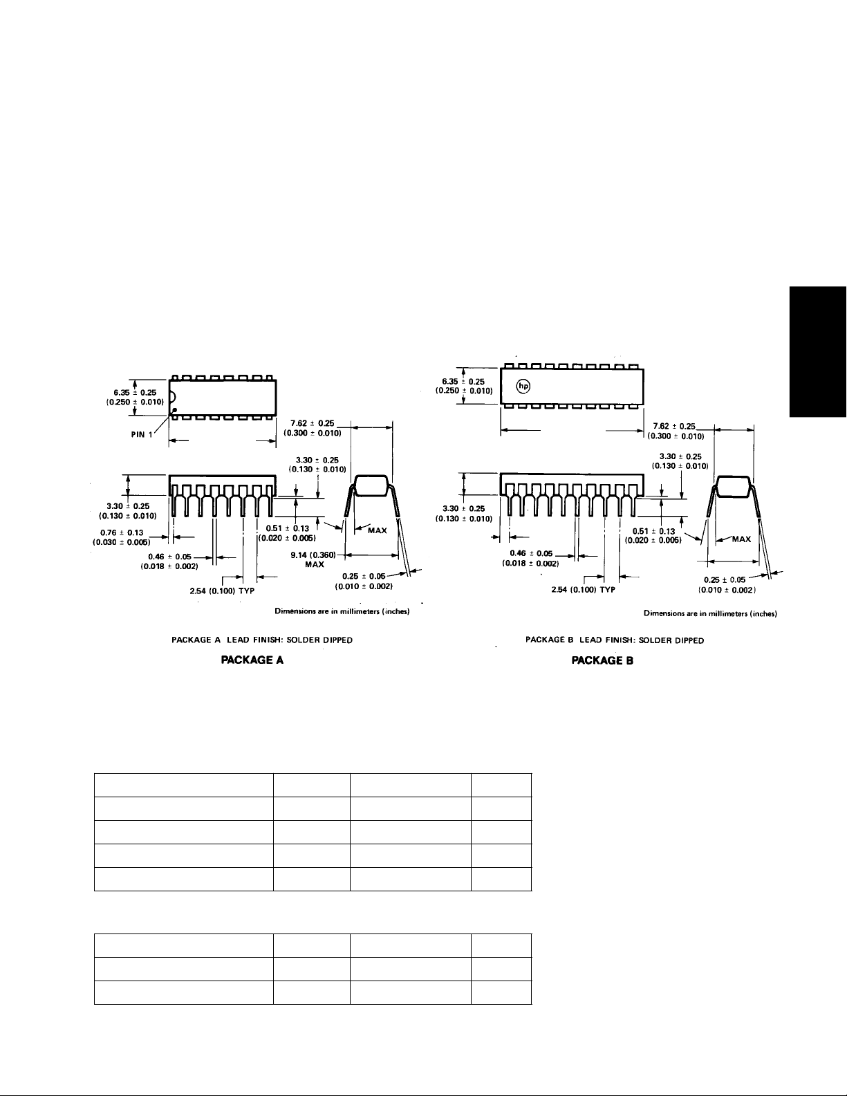
Part Number Description Package Drawing
HCTL-2000 12-bit counter. 14 MHz clock operation. A
HCTL-2016 All features of the HCTL-2000. 16-bit counter. A
HCTL-2020 All features of the HCTL-2016. Quadrature decoder output B
signals. Cascade output signals.
ESD WARNING: Standard CMOS handling precautions should be observed with the HCTL-20XX family
ICs.
2-178
5965-5894E
Page 2
in digital closed loop motion
control systems and digital data
input systems. It does this by
shifting time intensive quadrature
decoder functions to a cost
effective hardware solution. The
entire HCTL-20XX family consists of a 4x quadrature decoder,
a binary up/down state counter,
Package Dimensions
19.05 ± 0.25
(0.750 ± 0.010)
and an 8-bit bus interface. The
use of Schmitt-triggered CMOS
inputs and input noise filters
allows reliable operation in noisy
environments. The HCTL-2000
contains a 12-bit counter. The
HCTL-2016 and 2020 contain a
16-bit counter. The HCTL-2020
also contains quadrature decoder
output signals and cascade
signals for use with many
standard counter ICs. The HCTL20XX family provides LSTTL
compatible tri-state output
buffers. Operation is specified for
a temperature range from -40 to
+85°C at clock frequencies up to
14 MHz.
25.91 ± 0.25
(1.02 ± 0.010)
AND CONTROL
MOTION SENSING
Operating Characteristics
Table 1. Absolute Maximum Ratings
(All voltages below are referenced to VSS)
Parameter Symbol Limits Units
DC Supply Voltage V
Input Voltage V
Storage Temperature T
Operating Temperature T
DD
A
IN
S
[1]
15°
1.52 ± 0.13
(0.060 ± 0.005)
-0.3 to +5.5 V
-0.3 to VDD +0.3 V
-40 to +125 °C
-40 to +85 °C
15°
9.40 (0.370)
Table 2. Recommended Operating Conditions
Parameter Symbol Limits Units
DC Supply Voltage V
Ambient Temperature T
A
DD
[1]
+4.5 to +5.5 V
-40 to +85 °C
2-179
Page 3
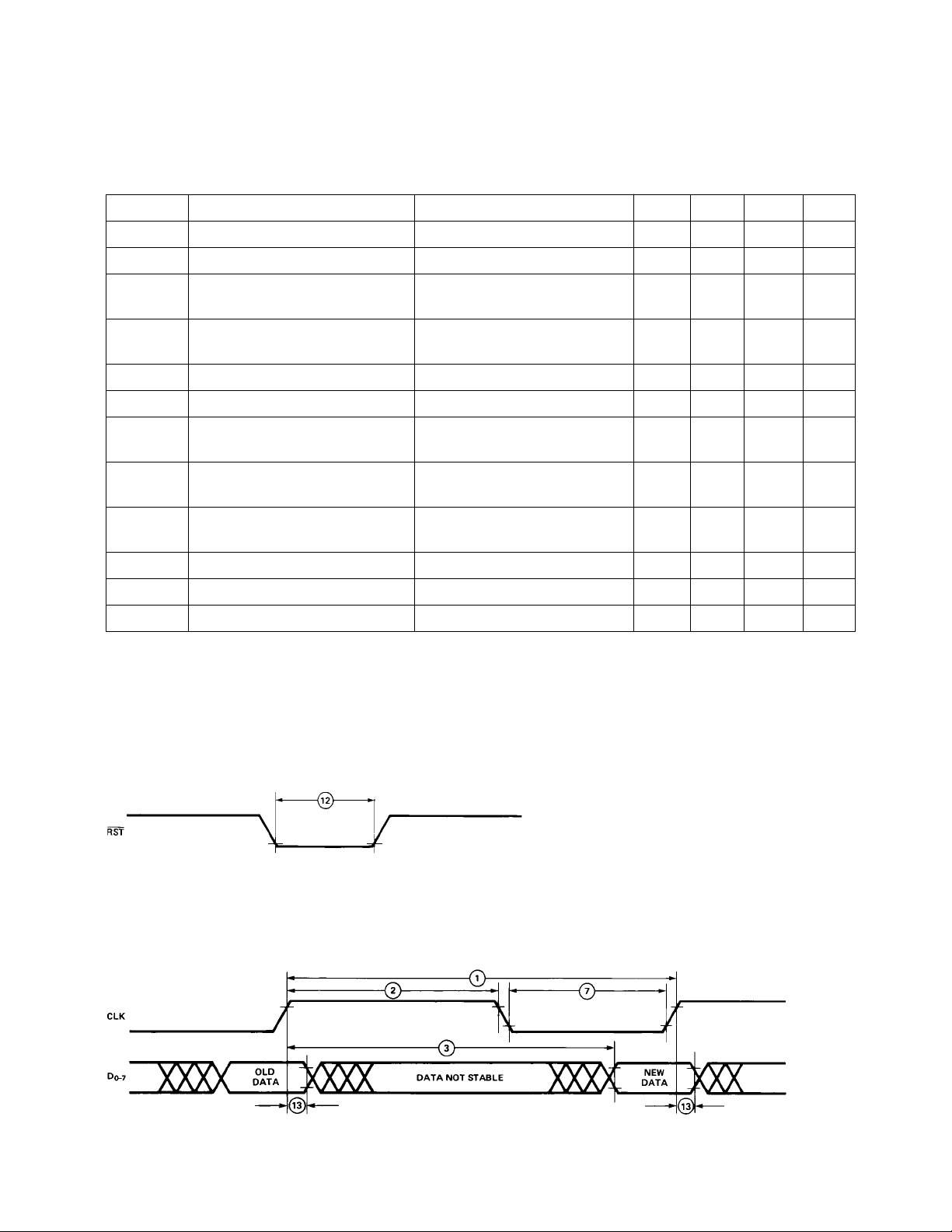
Table 3. DC Characteristics VDD = 5 V ± 5%; TA = -40 to 85°C
Symbol Parameter Condition Min. Typ. Max. Unit
[2]
V
IL
[2]
V
IH
V
T+
Low-Level Input Voltage 1.5 V
High-Level Input Voltage 3.5 V
Schmitt-Trigger Positive- 3.5 4.0 V
Going Threshold
V
T-
Schmitt-Trigger Negative- 1.0 1.5 V
Going Threshold
V
H
I
IN
V
OH
Schmitt-Trigger Hysteresis 1.0 2.0 V
Input Current VIN = VSS or V
[2]
High-Level Output IOH -1.6 mA 2.4 4.5 V
DD
-10 1 +10 µA
Voltage
[2]
V
OL
Low-Level Output IOL = +4.8 mA 0.2 0.4 V
Voltage
I
OZ
High-Z Output Leakage VO = V
SS
or V
DD
-10 1 +10 µA
Current
I
DD
C
IN
C
OUT
Notes:
1. Free air.
2. In general, for any VDD between the allowable limits (+4.5 V to +5.5 V), VIL = 0.3 VDD and VIH = 0.7 VDD; typical values are
VOH= VDD - 0.5 V @ I
3. Including package capacitance.
Quiescent Supply Current VIN = VSS or VDD, VO = HiZ 1 5 µA
= 1.6 mA.
OL
[3]
[3]
5pF
6pF
Input Capacitance Any Input
Output Capacitance Any Output
= -40 µA and VOL = VSS + 0.2 V @ I
OH
Figure 1. Reset Waveform.
Figure 2. Waveform for Positive Clock Related Delays.
2-180
Page 4

Functional Pin Description
Table 4. Functional Pin Descriptions
Pin Pin
Symbol 2000/2016 2020 Description
V
DD
V
SS
16 20 Power Supply
8 10 Ground
CLK 2 2 CLK is a Schmitt-trigger input for the external clock signal.
CHA 7 9 CHA and CHB are Schmitt-trigger inputs which accept the outputs
CHB 6 8 from a quadrature encoded source, such as incremental optical shaft
encoder. Two channels, A and B, nominally 90 degrees out of phase,
are required.
RST 5 7 This active low Schmitt-trigger input clears the internal position
counter and the position latch. It also resets the inhibit logic. RST is
asynchronous with respect to any other input signals.
OE 4 4 This CMOS active low input enables the tri-state output buffers. The
OE and SEL inputs are sampled by the internal inhibit logic on the
falling edge of the clock to control the loading of the internal position
data latch.
SEL 3 3 This CMOS input directly controls which data byte from the position
latch is enabled into the 8-bit tri-state output buffer. As in OE above,
SEL also controls the internal inhibit logic.
SEL BYTE SELECTED
0 High
1 Low
AND CONTROL
MOTION SENSING
CNT
DCDR
16 A pulse is presented on this LSTTL-compatible output when the
quadrature decoder has detected a state transition.
U/D 5 This LSTTL-compatible output allows the user to determine whether
the IC is counting up or down and is intended to be used with the
CNT
CAS
CNT
(low level) will be present before the rising edge of the CNT
CNT
15 A pulse is presented on this LSTTL-compatible output when the
DCDR
outputs.
CAS
and CNT
outputs. The proper signal U (high level) or D
CAS
DCDR
HCTL-2020 internal counter overflows or underflows. The rising edge
on this waveform may be used to trigger an external counter.
D0 1 1
D1 15 19
D2 14 18
D3 13 17
These LSTTL-compatible tri-state outputs form an 8-bit output port
through which the contents of the 12/16-bit position latch may be read in
2 sequential bytes. The high byte, containing bits 8-15, is read first (on the
HCTL-2000, the most significant 4 bits of this byte are set to 0 internally).
The lower byte, bits 0-7, is read second.
D4 12 14
D5 11 13
D6 10 12
D7 9 11
NC 6 Not connected - this pin should be left floating.
and
2-181
Page 5
Switching Characteristics
Table 5. Switching Characteristics Min/Max specifications at VDD = 5.0 ± 5%, TA = -40 to + 85°C.
Symbol Description Min. Max. Units
1t
2t
3t
4t
5t
6t
7t
8t
9t
10 t
11 t
12 t
13 t
14 t
15 t
16 t
17 t
18 t
19 t
20 t
21 t
CLK
CHH
CD
ODE
ODZ
SDV
CLH
SS
OS
SH
OH
RST
DCD
DSD
DOD
UDD
CHD
CLD
UDH
UDCS
UDCH
Clock period 70 ns
Pulse width, clock high 28 ns
[1]
Delay time, rising edge of clock to valid, updated count 65 ns
information on D0-7
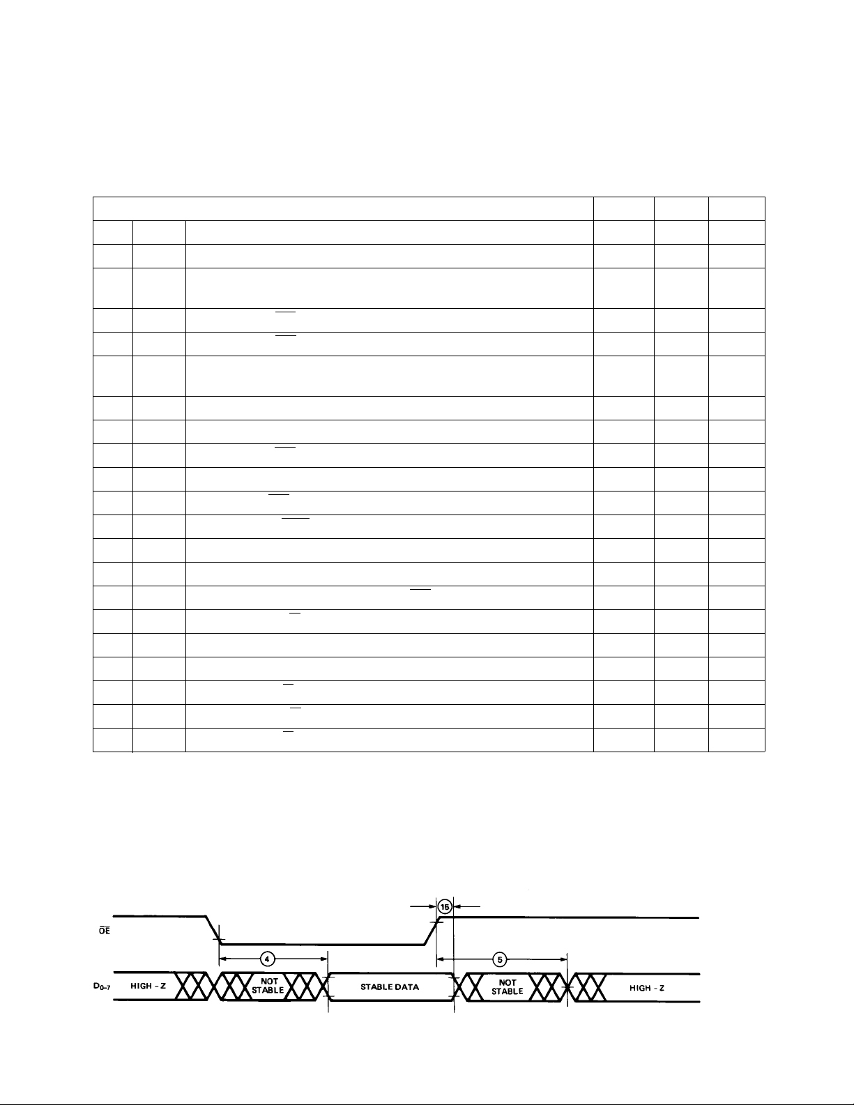
Delay time, OE fall to valid data 65 ns
Delay time, OE rise to Hi-Z state on D0-7 40 ns
Delay time, SEL valid to stable, selected data byte 65 ns
(delay to High Byte = delay to Low Byte)
Pulse width, clock low 28 ns
[2]
Setup time, SEL before clock fall 20 ns
[2]
Setup time, OE before clock fall 20 ns
[2]
Hold time, SEL after clock fall 0 ns
[2]
Hold time, OE after clock fall 0 ns
Pulse width, RST low 28 ns
Hold time, last position count stable on D0-7 after clock rise 10 ns
Hold time, last data byte stable after next SEL state change 5 ns
Hold time, data byte stable after OE rise 5 ns
Delay time, U/D valid after clock rise 45 ns
Delay time, CNT
Delay time, CNT
DCDR
DCDR
or CNT
or CNT
high after clock rise 45 ns
CAS
low after clock fall 45 ns
CAS
Hold time, U/D stable after clock rise 10 ns
Setup time, U/D valid before CNT
Hold time, U/D stable after CNT
DCDR
DCDR
or CNT
or CNT
rise t
CAS
rise t
CAS
-45 ns
CLK
-45 ns
CLK
Notes:
1. tCD specification and waveform assume latch not inhibited.
2. tSS, tOS, tSH, tOH only pertain to proper operation of the inhibit logic. In other cases, such as 8 bit read operations, these setup
and hold times do not need to be observed.
Figure 3. Tri-State Output Timing.
2-182
Page 6

Figure 4. Bus Control Timing.
Figure 5. Decoder, Cascade Output Timing (HCTL-2020 only).
AND CONTROL
MOTION SENSING
2-183
Page 7

Operation
A block diagram of the HCTL20XX family is shown in Figure 6.
The operation of each major
function is described in the
following sections.
Figure 6. Simplified Logic Diagram.
Digital Noise Filter
The digital noise filter section is
responsible for rejecting noise on
the incoming quadrature signals.
The input section uses two
techniques to implement
improved noise rejection.
Schmitt-trigger inputs and a
three-clock-cycle delay filter
combine to reject low level noise
and large, short duration noise
spikes that typically occur in
motor system applications. Both
common mode and differential
mode noise are rejected. The user
benefits from these techniques by
improved integrity of the data in
2-184
the counter. False counts
triggered by noise are avoided.
Figure 7 shows the simplified
schematic of the input section.
The signals are first passed
through a Schmitt trigger buffer
to address the problem of input
signals with slow rise times and
low level noise (approximately
< 1 V). The cleaned up signals
are then passed to a four-bit
delay filter. The signals on each
channel are sampled on rising
clock edges. A time history of the
signals is stored in the four-bit
shift register. Any change on the
input is tested for a stable level
being present for three
consecutive rising clock edges.
Therefore, the filtered output
waveforms can change only after
an input level has the same value
for three consecutive rising clock
edges. Refer to Figure 8 which
shows the timing diagram. The
result of this circuitry is that
short noise spikes between rising
clock edges are ignored and
pulses shorter than two clock
periods are rejected.
Page 8

Figure 7. Simplified Digital Noise Filter Logic.
Figure 8. Signal Propagation through Digital Noise Filter.
AND CONTROL
MOTION SENSING
Quadrature Decoder
The quadrature decoder decodes
the incoming filtered signals into
count information. This circuitry
multiplies the resolution of the
input signals by a factor of four
(4X decoding). When using an
encoder for motion sensing, the
user benefits from the increased
resolution by being able to
provide better system control.
The quadrature decoder samples
the outputs of the CHA and CHB
filters. Based on the past binary
state of the two signals and the
present state, it outputs a count
signal and a direction signal to
the internal position counter. In
the case of the HCTL-2020, the
signals also go to external pins 5
and 16 respectively.
Figure 9 shows the quadrature
states and the valid state transitions. Channel A leading channel
B results in counting up. Channel
B leading channel A results in
counting down. Illegal state
transitions, caused by faulty
encoders or noise severe enough
to pass through the filter, will
produce an erroneous count.
Design Considerations
The designer should be aware
that the operation of the digital
filter places a timing constraint
on the relationship between
incoming quadrature signals and
the external clock. Figure 8
shows the timing waveform with
an incremental encoder input.
Since an input has to be stable
for three rising clock edges, the
encoder pulse width (tE - low or
high) has to be greater than three
clock periods (3t
guarantees that the asynchronous
input will be stable during three
consecutive rising clock edges. A
realistic design also has to take
CLK
). This
2-185
Page 9

into account finite rise times of
the waveforms, asymmetry of the
waveforms, and noise. In the
presence of large amounts of
noise, tE should be much greater
than 3t
to allow for the
CLK
interruption of the consecutive
level sampling by the three-bit
delay filter. It should be noted
that a change on the inputs that
is qualified by the filter will
internally propagate in a maximum of seven clock periods.
The quadrature decoder circuitry
imposes a second timing constraint between the external clock
and the input signals. There must
be at least one clock period
between consecutive quadrature
states. As shown in Figure 9, a
quadrature state is defined by
consecutive edges on both
channels. Therefore, tES (encoder
state period) > t
CLK
. The
designer must account for
deviations from the nominal 90
degree phasing of input signals to
guarantee that tES > t
CLK
.
Position Counter
This section consists of a 12-bit
(HCTL-2000) or 16-bit (HCTL2016/2020) binary up/down
counter which counts on rising
clock edges as explained in the
Quadrature Decoder Section. All
12 or 16 bits of data are passed
to the position data latch. The
system can use this count data in
several ways:
A. System total range is ≤ 12 or
16 bits, so the count represents “absolute” position.
B. The system is cyclic with ≤
12 or 16 bits of count per
cycle. RST is used to reset
the counter every cycle and
the system uses the data to
interpolate within the cycle.
C. System count is > 8, 12, or 16
bits, so the count data is
used as a relative or incremental position input for a
system software computation
of absolute position. In this
case counter rollover occurs.
In order to prevent loss of
position information, the
processor must read the
outputs of the IC before the
count increments one-half of
the maximum count capabil-
ity (i.e. 127. 2047, or 32,767
quadrature counts). Two’scomplement arithmetic is
normally used to compute
position from these periodic
position updates. Three
modes can be used:
1. The IC can be put in 8-bit
mode by tying the SEL
line high, thus simplifying IC interface. The
outputs must then be
read at least once every
127 quadrature counts.
2. The HCTL-2000 can be
used in 12-bit mode and
sampled at least once
every 2047 quadrature
counts.
3. The HCTL-2016 or 2020
can be used in 16-bit
mode and sampled at
least once every 32,767
quadrature counts.
D. The system count is > 16 bits
so the HCTL-2020 can be
cascaded with other standard counter ICs to give
absolute position.
Position Data Latch
The position data latch is a 12/
16-bit latch which captures the
position counter output data on
each rising clock edge, except
when its inputs are disabled by
the inhibit logic section during
two-byte read operations. The
output data is passed to the bus
interface section. When active, a
signal from the inhibit logic
section prevents new data from
being captured by the latch,
keeping the data stable while
successive reads are made
through the bus section. The
latch is automatically reenabled
at the end of these reads. The
latch is cleared to 0 asynchronously by the RST signal.
Figure 9. 4x Quadrature Decoding.
2-186
Page 10

Inhibit Logic
The Inhibit Logic Section samples
the OE and SEL signals on the
falling edge of the clock and, in
response to certain conditions
(see Figure 10 below), inhibits
the position data latch. The RST
output and whether or not the
output bus is in the high-Z state.
In the case of the HCTL-2000 the
data latch is only 12 bits wide
and the upper four bits of the
high byte are internally set to
zero.
signal asynchronously clears the
inhibit logic, enabling the latch. A
simplified logic diagram of the
inhibit circuitry is illustrated in
Figure 11.
Quadrature Decoder Output (HCTL-2020 Only)
The quadrature decoder output
section consists of count and up/
Bus Interface
The bus interface section consists
of a 16 to 8 line multiplexer and
an 8-bit, three-state output
buffer. The multiplexer allows
independent access to the low
and high bytes of the position
data latch. The SEL and OE
signals determine which byte is
down outputs derived from the
4X decode logic of the HCTL-
2020. When the decoder has
detected a count, a pulse, onehalf clock cycle long, will be
output on the CNT
DCDR
output will occur during the clock
cycle in which the internal
counter is updated. The U/D pin
Inhibit
Step SEL OE CLK Signal Action
1 L L 1 Set inhibit; read high byte
2 H L 1 Read low byte; starts reset
3 X H 0 Completes inhibit logic reset
pin. This
will be set to the proper voltage
level one clock cycle before the
rising edge of the CNT
DCDR
pulse, and held one clock cycle
after the rising edge of the
CNT
pulse. These outputs
DCDR
are not affected by the inhibit
logic. See Figures 5 and 12 for
detailed timing.
Cascade Output (HCTL2020 Only)
The cascade output also consists
of count and up/down outputs.
When the HCTL-2020 internal
counter overflows or underflows,
a pulse, one-half clock cycle long,
will be output on the CNT
This output will occur during the
clock cycle in which the internal
counter is updated. The U/D pin
will be set to the proper voltage
level one clock cycle before the
rising edge of the CNT
and held one clock cycle after the
rising edge of the CNT
These outputs are not affected by
the inhibit logic. See Figures 5
and 12 for detailed timing.
CAS
CAS
pin.
CAS
pulse,
pulse.
AND CONTROL
MOTION SENSING
Figure 10. Two Byte Read Sequence.
Figure 11. Simplified Inhibit Logic.
2-187
Page 11

CHA
CHB
CNT
CNT
CLK
FILT
FILT
DCDR
CAS
U/D
INTERNAL COUNTER
ROLL OVER
00
FF
*
START INHIBIT
*
*
COUNT
*CHA
AND CHB
FILT
OF THE DIGITAL NOISE FILTER (SEE FIGURES 7 AND 8).
Figure 12. Decode and Cascade Output Diagram.
FILT
Cascade Considerations (HCTL-2020 Only)
The HCTL-2020’s cascading
system allows for position reads
of more than two bytes. These
reads can be accomplished by
latching all of the bytes and then
reading the bytes sequentially
over the 8-bit bus. It is assumed
here that, externally, a counter
followed by a latch is used to
count any count that exceeds 16
bits. This configuration is
compatible with the HCTL-2020
internal counter/latch
combination.
FFFDH FFFEH FFFFH 0000H FFFFH FFFDH
ARE THE OUTPUTS
will be generated with some delay
after the rising clock edge (t
There will be additional
propagation delays through the
external counters and registers.
Meanwhile, with SEL and OE low
to start the read, the internal
latches are inhibited at the falling
edge and do not update again till
the inhibit is reset. If the CNTCAS
pulse now toggles the external
counter and this count gets
latched a major count error will
occur. The count error is because
the external latches get updated
when the internal latch is
inhibited.
Consider the sequence of events
for a read cycle that starts as the
HCTL-2020’s internal counter
rolls over. On the rising clock
edge, count data is updated in the
internal counter, rolling it over. A
count-cascade pulse (CNT
CAS
)
Valid data can be ensured by
latching the external counter data
when the high byte read is started
(SEL and OE low). This latched
external byte corresponds to the
CHD
count in the inhibited internal
).
latch. The cascade pulse that
occurs during the clock cycle
when the read begins gets
counted by the external counter
and is not lost.
For example, suppose the HCTL2020 count is at FFFFH and an
external counter is at F0H, with
the count going up. A count
occurring in the HCTL-2020 will
cause the counter to roll over and
a cascade pulse will be generated.
A read starting on this clock cycle
will show FFFFH from the HCTL-
2020. The external latch should
read F0H, but if the host latches
the count after the cascade signal
propagates through, the external
latch will read F1H.
2-188
Page 12

General Interfacing
The 12-bit (HCTL-2000) or 16-bit
(HCTL-2016/2020) latch and
inhibit logic allows access to 12
or 16 bits of count with an 8-bit
bus. When only 8-bits of count
are required, a simple 8-bit (1byte) mode is available by
holding SEL high continuously.
This disables the inhibit logic. OE
provides control of the tri-state
bus, and read timing is shown in
Figures 2 and 3.
For proper operation of the
inhibit logic during a two-byte
read, OE and SEL must be
synchronous with CLK due to
the falling edge sampling of OE
and SEL.
The internal inhibit logic on the
HCTL-20XX family inhibits the
transfer of data from the counter
to the position data latch during
the time that the latch outputs are
being read. The inhibit logic
allows the microprocessor to first
read the high order 4 or 8 bits
from the latch and then read the
low order 8 bits from the latch.
Meanwhile, the counter can
continue to keep track of the
quadrature states from the CHA
and CHB input signals.
Figure 11 shows the simplified
inhibit logic circuit. The
operation of the circuitry is
illustrated in the read timing
shown in Figure 13.
AND CONTROL
MOTION SENSING
Figure 13. Typical Interface Timing.
*OE can consist of two short low pulses, as well as one long pulse, and still satisfy
the inhibit logic sequence. During the time that OE is high, the data lines are tri-seated.
2-189
Page 13

Actions
1. On the rising edge of the clock,
counter data is transferred to
the position data latch,
provided the inhibit signal is
low.
2. When OE goes low, the
outputs of the multiplexer are
enabled onto the data lines. If
SEL is low, then the high order
data bytes are enabled onto the
data lines. If SEL is high, then
the low order data bytes are
enabled onto the data lines.
3. When the IC detects a low on
OE and SEL during a falling
clock edge, the internal inhibit
signal is activated. This blocks
new data from being
transferred from the counter to
the position data latch.
4. When SEL goes high, the data
outputs change from the high
byte to the low byte.
5. The first of two reset conditions for the inhibit logic is
met when the IC detects a
logic high on SEL and a logic
low on OE during a falling
clock edge.
6. When OE goes high, the data
lines change to a high impedance state.
7. The IC detects a logic high on
OE during a falling clock edge.
This satisfies the second reset
condition for the inhibit logic.
2-190
Page 14

Interfacing the HCTL-2020 to a Motorola 6802/8 and Cascading the Counter for 24 Bits
AND CONTROL
MOTION SENSING
Figure 14. A Circuit to Interface to the 6802/8.
2-191
Page 15

In this circuit an interface to a
Motorola 6802/8 and a cascading
scheme for a 24-bit counter are
shown. This circuit provides a
minimum part count by: 1) using
two 74LS697 Up/Down counters
with output registers and tri-state
outputs and 2) using a Motorola
6802/8 LDX instruction which
stores 16 bits of data into the
index registers in two consecutive
clock cycles.
The HCTL-2020 OE and the
74LS697 G lines are decoded
from Address lines A15-A13. This
results in counter data being
enabled onto the bus whenever
an external memory access is
made to locations 4XXX or 2XXX.
Address line A12 and processor
clock E enables the 74LS138.
The processor clock E is also
used to clock the HCTL-2020.
Address AO is connected directly
to the SEL pin on the HCTL-
2020. This line selects the low or
high byte of data from the HCTL-
2020.
Cascading is accomplished by
connecting the CNT
output on
CAS
the HCTL-2020 with the counter
clock (CCK) input on both
74LS697s. The U/D pin on the
HCTL-2020 and the U/D pin on
both 74LS697s are also directly
connected for easy expansion.
The RCO of the first 4-bit
74LS697 is connected to the ENT
pin of the second 74LS697. This
enables the second counter only
when there is a RCO signal on the
first counter.
This configuration allows the
6802 to read both data bytes with
a single double-byte fetch
instruction (LDX 2XX0). This
instruction is a five cycle
instruction which reads external
memory location 2XX0 and stores
the high order byte into the high
byte of the index register.
Memory location 2XX1 is next
read and stored in the low order
byte of the index register. The
high byte of counter data is
clocked into the 74LS697
registers when SEL is low and
OE goes low. This upper byte can
be read at any time by pulling the
74LS697 G low when reading
address 4XXX. Figure 15 shows
memory addresses and gives an
example of reading the HCTL-
2020. Figure 16 shows the
interface timing for the circuit.
Address Function
CXXX Reset Counters
4XXX Enable High Byte on Data Lines
2XX0 Enable Mid Byte on Data Lines
2XX1 Enable Low Byte on Data Lines
Read Example
LDX 2000 Loads mid byte and then low byte into
STX 0100 memory locations 0100 and 0101
LDAA 4000 Loads the high byte into memory
STAA 0102 location 0102
Figure 15. Memory Addresses and Read Example.
2-192
Page 16

HCTL-2020
INTERNAL CLOCK
CLK
SEL
OE
INTERNAL
INHIBIT
CNT
CAS
RCK
G
FFFF 0000
AND CONTROL
MOTION SENSING
DATA
HIGH Z
BUS
ACTIONS
Figure 16. Interface Timing for the 6802/8.
11 1
Actions
1. The microprocessor clock
output is E. If the internal
HCTL-2020 inhibit is not
active, new data is transferred from the internal
counter to the position data
latch.
2. An even address output
from the 6802 causes SEL to
go low. When E goes high,
the address decoder output
for the HCTL-2020 OE
signal goes low. This causes
the HCTL-2020 to output
the middle byte of the
system counter (high byte of
the HCTL-2020 counter).
This middle byte, FFFFH is
available at (2) through (4),
the first time OE is low. In
this example an overflow
MID
BYTE
4 5
3
2
LOW
BYTE
7 8 9 10
6
has occurred and OE has
been pulled low to start a
read cycle. SEL and OE are
gated to give RCK which
latches the external high
byte, equal to 00H. The
falling edge, of the CNT
CAS
signal counts up the
external counter to 0001H.
3. With the first negative edge
of the clock after SEL and
OE are low the internal
latches are inhibited from
counting and the 6802 reads
the high byte in.
4. OE goes high and the data
bus goes into a high
impedance state.
5. OE is low and SEL is high
and the low byte is enabled
onto the data bus. The low
byte is valid through (7).
HIGH
BYTE
6. With the first negative edge
after OE and SEL go high,
the first of the two HCTL2020 inhibit reset conditions
is met and the 6802 reads
the low byte in.
7. The data bus returns to the
high impedance state, when
OE goes high.
8. With the first negative edge
of the clock after OE goes
high, inhibit reset is
complete.
9. With the positive going edge
of the clock, G is asserted
and the external high byte,
00H is available on the data
bus from 9 through 10 and
the 6802 reads the high byte
in at (10).
2-193
Page 17

Interfacing the HCTL20XX to an Intel 8748
The circuit shown in Figure 17
shows the connections between
an HCTL-20XX and an 8748.
Data lines D0-D7 are connected
to the 8748 bus port. Bits 0 and 1
of port 1 are used to control the
OE and SEL inputs of the HCTL20XX respectively. T0 is used to
provide a clock signal to the
HCTL-20XX. The frequency of T0
is the crystal frequency divided
by 3. T0 must be enabled by
executing the ENT0 CLK
instruction after each system
reset, but prior to the first
encoder position change. An
8748 program which interfaces
to the circuit in Figure 17 is
given in Figure 18. The resulting
interface timing is shown in
Figure 19.
* NOTE: PIN NUMBERS ARE DIFFERENT FOR THE HCTL-2020.
Figure 17. An HCTL-20XX-to-Intel 8748 Interface.
Object Source
LOC Code Statements Comments
000 99 00 ANL P1, 00H Enable output and higher order
bits
002 08 INS A, BUS Load higher order bits into ACC
003 A8 MOVE R0, A Move data to register 0
004 89 02 ORL P1, 02H Enable output and lower order
bits
006 08 INS A, BUS Load order bits into AC
008 A9 MOV R1, A Move data to register 1
009 89 03 ORL P1, 03H Disable outputs
00B 93 RETR Return
Figure 18. A Typical Program for Reading HCTL-20XX with an 8748.
2-194
Page 18

ANL P1, OOH
Figure 19. 8748 READ Cycle from Figure 18.
ORL P1, 02H
AND CONTROL
MOTION SENSING
Actions
1. ANL P1, 00H has just been
executed. The output of bits 0
and 1 of Port 1 cause SEL and
OE to be logic low. The data
lines output the higher order
byte.
2. The HCTL-20XX detects that
OE and SEL are low on the
next falling edge of the CLK
and asserts the internal inhibit
signal. Data can be read
without regard for the phase of
the CLK.
3. INS A, BUS has just been
executed. Data is read into the
8748.
4. ORL PORT 1, 02H has just
been executed. The program
sets SEL high and leaves OE
low by writing the correct
values to port 1. The HCTL-
20XX detects OE is low and
SEL is high on the next falling
edge of the CLK, and thus the
first inhibit reset condition is
met.
5. INS A, BUS has just been
executed. Lower order data
bits are read into the 8748.
6. ORL P1, 03H has just been
executed. The HCTL-20XX
detects OE high on the next
falling edge of CLK. The
program sets OE and SEL high
by writing the correct values to
port 1. This causes the data
lines to be tristated. This
satisfies the second inhibit and
reset condition. On the next
rising CLK edge new data is
transferred from the counter to
the position data latch.
Additional Information from Hewlett-Packard
Application briefs are available
from the factory. Please contact
your local HP sales representative
for the following.
M027 Interfacing the HCTL-20XX
to the 8051
M019 Commonly Asked
Questions about the HCTL2020 and Answers
M020 A Simple Interface for the
HCTL-2020 with a 16-bit
DAC without Using a
Processor
M023 Interfacing the MC68HCII
to the HCTL-2020
2-195
 Loading...