

Optical Reflective Sensors
Technical Data
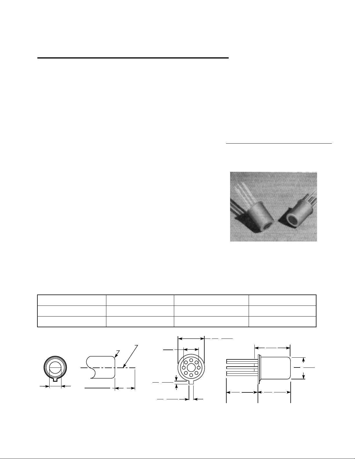
hH
HBCC-1570
HBCC-1580
HBCC-1590
Features
• Focused Emitter and
Detector in a Single
Package
• TO-5 Miniature Sealed
Package
• Photodiode Output
• Choice of Resolutions
(0.13 mm, 0.178 mm, 0.33 mm)
• Two Wavelengths
Available; 655 nm, 820 nm
(see selection guide)
Description
The HBCC-15XX series sensors
are fully integrated modules
designed for applications requiring optical reflective sensing. The
modules contain a 655 nm (or 820
nm) LED emitter and a photodiode. A bifurcated aspheric lens
is used to image the active areas
of the emitter and detector to a
single spot 4.27 mm (0.168 in.) in
front of the package. The output
signal is a current generated by
the photodiode.
Applications
The HBCC-15XX sensors are
intended for use with the HewlettPackard HBCC-0500 and HBCC0600 low current digitizer ICs, or
Selection Guide
Sensor Part Number HBCC-1570 HBCC-1580 HBCC-1590
LED Resolution 0.33 mm (0.013 in.) 0.185 mm (0.007 in.) 0.13 mm (0.005 in.)
LED Wavelength 655 nm 655 nm 820 nm
Package Dimensions
MAXIMUM SIGNAL POINT – MSP
REFERENCE PLANE
5.08
(0.200)
9.40
8.51
(0.370)
(0.335)
S.P.
12.0
(0.473)
R.P.
O.D.
C
L
5.08
(0.200)
NOTES:
A. ALL DIMENSIONS IN MILLIMETERS AND (INCHES).
B. ALL UNTOLERANCED DIMENSIONS ARE FOR REFERENCE ONLY.
C. THE REFERENCE PLANE (R.P.) IS THE TOP SURFACE OF THE PACKAGE.
D. NICKEL CAN AND GOLD PLATED LEADS.
(0.168) ± (0.010)
4.27
0.25
±
Z
5965-5942E
1.14
0.73
0.86
0.73
(0.045)
(0.029)
(0.034)
(0.029)
E. S.P. = SEATING PLANE.
F. THE LEAD DIAMETER IS 0.45 mm (0.018 in.) TYP.
G. O.D. = OUTSIDE DIAMETER OF CAN MEASURED IN REGION ABOVE
WELD FLANGE TO MIDWAY OF CAN LENGTH.
15.24
12.70
(0.600)
(0.500)
11.50
11.22
(0.453)
(0.442)
8.33
8.12
(0.328)
(0.320)
4-7
with suitable PCB assemblies
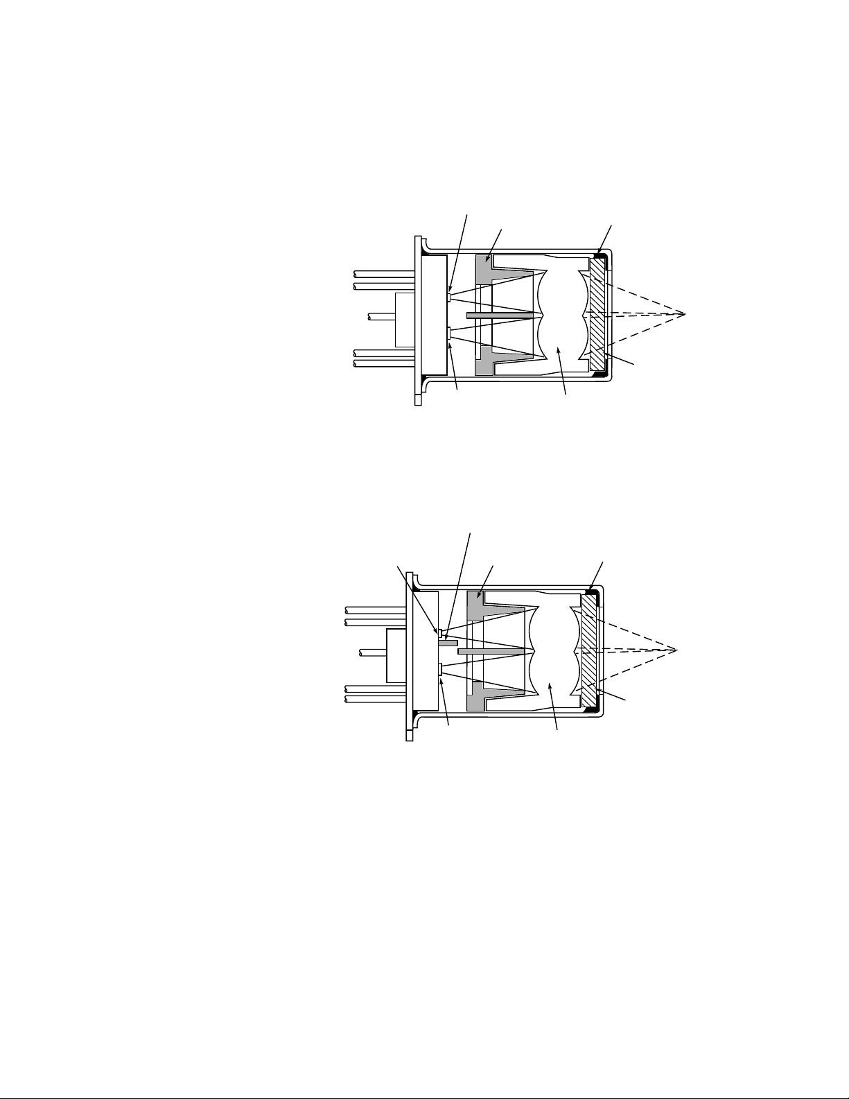
EMITTER
BAFFLE
EPOXY SEAL
SENSING
AREA
GLASS
LENS
DETECTOR
provided by HP for use with these
sensors. The HBCC-15XX sensors
have been characterized for use
only with Hewlett-Packard’s
digitizer IC technology. Use of
these sensors in designs or applications other than those stated is
at the customer’s risk.
Mechanical Considerations
The HBCC-15XX series are
packaged in a high profile 8 pin
TO-5 metal can with a glass
window. The LED and photodiode
are mounted on a header at the
base of the package. Positioned
above these active elements is a
bifurcated aspheric acrylic lens
that focuses them to the same
point.
The sensor can be rigidly secured
by commercially available TO-5
style heat sinks or 8 pin 0.200 inch
diameter pin circle sockets. These
fixtures provide a stable reference
platform for affixing the HBCC15XX sensors to a circuit board.
HBCC-1570, 1580 Optical System
HBCC-1590 Optical System
SILICON
BAFFLE
EMITTER
0.089 mm DIA. JUNCTION
OPTICAL
APERTURE
BAFFLE
EPOXY SEAL
SENSING
AREA
In applications requiring contact
scanning (such as bar code
reading), protective focusing tips
are available. Focusing tips are
available in either metal or polycarbonate packages using a
sapphire ball as the contact
surface. The Hewlett-Packard part
numbers are HBCS-2999, HBCS4999, HBCS-A998, and
HBCS-A999.
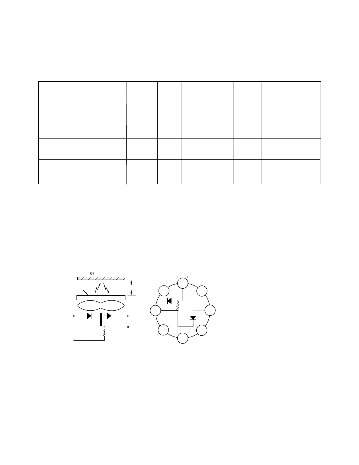
Electrical Operation
The sensor detector is a pn
photodiode. The LED cathode is
physically and electrically connected to the case-substrate of the
sensor.
4-8
DETECTOR
0.406 mm SQUARE
The HBCC-15XX sensors are
characterized for use with HewlettPackard’s low current digitizer
ICs. The digitizer IC part numbers
are HBCC-0500 and HBCC-0600.
Data Sheets including circuit
diagrams are available.
GLASS
LENS
Absolute Maximum Ratings
TA = 25°C unless specified otherwise (unless specified separately, data applies to all sensors)
Parameter Symbol Min. Max. Units Notes
Storage Temperature T
Operating Temperature T
S
A
Lead Soldering Temperature 260 °C1
(1.6 mm from Seating Plane) (for 10 seconds)
Average LED Forward Current I
Peak LED Forward Current I
Reverse LED Input Voltage V
Photodiode Bias V
Notes:
1. CAUTION: The thermal constraints of the acrylic lens will not permit conventional wave soldering procedures. The typical
preheat and post-soldering cleaning procedures and dwell times can subject lens to thermal stresses beyond the absolute
maximum ratings and can cause it to defocus.
2. These sensors are specified for use with the drive conditions provided by the HBCC-0500 and HBCC-0600 Digitizer IC ONLY.
3. When used with HBCC-0500 or HBCC-0600 digitizer ICs.
4. At all combinations of pulse width and duty cycle.
5. Voltage differential between Pin 1 and Pin 8 with Pin 8 taken as reference. Exceeding maximum conditions may cause permanent
damage to photodiode or to chip metallization.
f
fp
r
d
-40 +75 °C
-20 +75 °C
2
125 mA 3 (HBCC-1570)
100 mA 3 (HBCC-1580)
40 mA 4 (HBCC-1590)
5.0 V
2.5 V HBCC-1590 Only
-0.3 6.0 V 5
REFERENCE
PLANE
6
2
REFLECTOR
Z
LED
CASE, SUBSTRATE
SCHEMATIC DIAGRAM CONNECTION DIAGRAM
D
ps
R
s
Rs = CHARACTERISTIC NOT DEFINED
1
8
1
2
3
8
D
ps
R
s
+
4
TOP VIEW
7
LED
5
PIN#
1
6
2
6
8
FUNCTION
PHOTODIODE CATHODE
HEADER GROUND
LED ANODE
PHOTODIODE ANODE
4-9

HBCC-1570 and HBCC-1580: Electrical and Optical Characteristics
TA = 25°C
Parameter Symbol Min. Typ. Max. Units Conditions Note Figure
Reflected (see Bin Table) nA If = 70 mA 6,7 1,2A,
Photocurrent peak 4A, 4B, 5
Quality Factor <Q> 0.82 0.95 1.0 – If = 70 mA 6,8
Maximum Signal Z 4.11 4.27 4.42 mm If = 70 mA 6,9 1, 4A, 4B
Point (MSP) (0.162) (0.168) (0.174) (in.) peak
LED Forward V
Voltage
LED Reverse BVR 5.0 – – V Ir = 100 µA
Breakdown Voltage
Photodiode I
Dark Current
Photodiode C
Capacitance 60 – pF Vd = 1 V
LED Peak λ – 650 670 nm If = 35 mA DC 6A
Wavelength
Ipr Temperature K
Coefficient
System Optical d – 0.268 – mm 4.27 mm 11 7A
Step Response (0.0106) (in.) (Target from
(OSR) sensor)
HBCC-1570
(OSR) d – 0.154 – mm 4.27 mm 11 7B
HBCC-1580 (0.0061) (in.) (Target from
I
pr
peak
f
d
d
e
1.5 1.75 2.0 V If = 70 mA 3
– 60 1000 pA Vd = 5 V
– 100 – pF Vd = 0 V
– -0.006 – 1/°CI
= 35 mA DC 10
f
sensor)
Notes:
6. Measured from a reflector coated with 99% diffuse reflective white paint (Kodak 6080) positioned 4.27 mm (0.168 in.) from the
reference plane. Measured physically is the total photocurrent, Ipt, which consists of a signal (reflected from target) component,
Ipr, and a component induced by reflections internal to the sensor (stray), Ips. Ipt = Ipr + Ips. Specified is the reflected signal
component, Ipr.
7. See Bin Table
8. <Q> = Ipr/Ipt
9. Measured from reference plane (R.P.) of sensor.
10. Photocurrent variation with temperature varies with LED output which follows a natural exponential law:
Ip(T) = Ip(To)*exp[Ke(T-To)]
11. OSR is defined as the distance for a 10%-90% “step” response of Ipr as the sensor moves over an abrupt black-white edge, or from
opaque white to free space (no reflection).
4-10

HBCC-1590: Electrical and Optical Characteristics
TA = 25°C
Parameter Symbol Min. Typ. Max. Units Conditions Note Figure
Reflected (see Bin Table) nA If = 30 mA 6,7 1,2B,
Photocurrent peak 4C, 5
Quality Factor <Q> 0.82 0.95 1.0 – If = 30 mA 6,8
Maximum Signal Z 4.01 4.27 4.62 mm If = 30 mA 6,9 1, 4C
Point (MSP) (0.158) (0.168) (0.182) (in.) peak
LED Forward V
Voltage
LED Reverse BVR 2.5 – – V Ir = 100 µA
Breakdown Voltage
Photodiode I
Dark Current
Photodiode C
Capacitance 60 pF Vd = 1 V
LED Peak λ 805 820 835 nm If = 35 mA DC 6B
Wavelength
Ipr Temperature K
Coefficient
System Optical d – 0.140 – mm 4.27 mm 11 7C
Step Response – (0.0055) – (in.) (Target from
(OSR) sensor)
I
pr
peak
f
d
d
e
1.3 1.45 1.8 V If = 30 mA 3
– 60 1000 pA Vd = 5 V
– 100 – pF Vd = 0 V
– -0.005 – 1/°CI
= 35 mA DC 10
f
REFLECTOR
REFERENCE
PLANE
+V
f
6
LED
I
f
2
CASE, SUBSTRATE
Figure 1. Photocurrent Test Circuit.
Z
I
pt
D
ps
R
s
1
8
nA-METER
4-11

Bin Table
Ipr Limits (nA)
Bin# Min. Max.
1 160 225
2 215 270
3 255 313
4 300 375
5 360 440
6 430 555
Product Marking
The photocurrent binning of the
sensor is incorporated as part of
the product marking format. The
Bin # is represented as the last
number (N) on the last line of
marking.
HP
HBCC-15XX
XXXXXXXN
N = bin number
Bin Availability
The entire available distribution of
parts, appropriately marked, will
be shipped. Requests for individual bin selections cannot be
honored.
conditions and temperature. LED
degradation is minimized by the
drive conditions generated by both
the HBCC-0500 and HBCC-0600,
(when used as specified).
Warranty and Service
HP Optical Reflective Sensors are
warranted for a period of one year
after purchase covering defects in
material and workmanship.
Hewlett-Packard will repair or, at
its option, replace products that
prove to be defective in material or
workmanship under proper use
during the warranty period.
NO OTHER WARRANTIES ARE
EXPRESSED OR IMPLIED,
INCLUDING BUT NOT LIMITED
TO THE IMPLIED WARRANTIES
OF MERCHANT ABILITY AND
FITNESS FOR A PARTICULAR
PURPOSE. HEWLETT-PACKARD
IS NOT LIABLE FOR CONSEQUENTIAL DAMAGES.
For additional warranty or service
information please contact your
local Hewlett-Packard sales
representative or authorized
distributor.
Binning and Temperature Effects
Test algorithm bins units to the
lower bin number if a unit is in the
bin overlap region. Such units can
cross bin boundaries as temperature changes. (Ambient temperature affects LED efficiency slightly
and may cause several percentage
changes in Ipr.) Bin numbers are
for “reference only” and do not
constitute an absolute guarantee.
The output of all LEDs degrades
with time, depending on drive
4-12

1.6
1.4
1.2
1.0
0.8
– 70mA, 25°C
0.6
f
I
HBCC-1580
0.4
0.2
PHOTOCURRENT NORMALIZED AT
0
0 102030405060708090
HBCC-1570
If – FORWARD LED CURRENT, mA
Figure 2A. Typical Reflected
Photocurrent.
1.4
1.2
1.0
0.8
0.6
– 30mA, 25°C
f
I
0.4
0.2
PHOTOCURRENT NORMALIZED AT
100
0
0102030
If – FORWARD LED CURRENT, mA
Figure 2B. Typical HBCC-1590
Reflected Photocurrent.
2.0
1.8
1.6
HBCC-1580
1.4
1.2
1.0
– FORWARD VOLTAGE, V
f
V
0.8
0.6
40
HBCC-1570
HBCC-1590
0.1
0.01
0.001
If – FORWARD CURRENT, mA
1
Figure 3. Typical LED Forward Voltage
vs. Forward Current.
100
10
100
MIN MSP
80
60
40
PERCENT MSP SIGNAL
20
0
3.5
3.0
DISTANCE FROM SENSOR, mm
4.0
MEAN MSP
4.5
Figure 4A. HBCC-1570 Signal vs.
Distance from Sensor.
1.0
HBCC 1570
HBCC 1580
0.8
0.6
0.4
NORMALIZED TO PEAK
0.2
RESPONSE AT GIVEN WAVELENGTH
0
500
550
TYP. PEAK RESPONSIVITY
Po =0.34 AMPS/WATT
HBCC 1590
LOW-PASS FILTERING OF
AMBIENT LIGHT CAUSED
BY RED LENS
650
600 700 800
WAVELENGTH, nm
750 850
Figure 5. Relative Spectral
Response of Sensors.
MAX MSP
5.0
100
MIN MSP
80
60
40
PERCENT MSP SIGNAL
20
5.5
0
3.5
3.0
DISTANCE FROM SENSOR, mm
Figure 4B. HBCC-1580 Signal vs.
Distance from Sensor.
1.75
1.50
1.25
1.00
0.75
0.50
0.25
0
LIGHT OUTPUT, NORMALIZED TO 25°C VALUE
600
900
620 640 680
WAVELENGTH, nm
Figure 6A. Typical Spectral
Distribution of 655 nm LED.
4.0
4.5
-20°C
660
0°C
25°C
MEAN MSP
MAX MSP
5.0
70°C
100
MIN MSP
80
60
40
PERCENT MSP SIGNAL
20
5.5
0
3.0
4.0
3.5
DISTANCE FROM SENSOR, mm
Figure 4C. HBCC-1590 Signal vs.
Distance from Sensor.
1.4
1.2
1.0
0.8
0.6
0.4
0.2
0
LIGHT OUTPUT, NORMALIZED TO 25°C VALUE
700
740
780 820
WAVELENGTH, nm
Figure 6B. Typical Spectral
Distribution of 820 nm LED.
-40°C
4.5
25°C
860
MEAN MSP
MAX MSP
5.0
85°C
5.5
900
4-13

1.0
WHITE
0.8
0.6
0.4
d — SYSTEM RESPONSE — mm
0.2
PREFERRED ORIENTATION
0
3.0
NON-PREFERRED ORIENTATION
3.5
4.0
DISTANCE FROM SENSOR — mm
100%
90%
d
10%
0
NORMALIZED SIGNAL
4.5 5.0
BLACK
5.5
Figure 7A. HBCC-1570, System Optical Step Response Variation with Distance.
1.0
WHITE
100%
90%
0.8
d
Preferred Orientation
At maximum signal point (MSP)
when the sensor is in focus, the
orientation of the sensor is unimportant. However, as one moves
away from MSP (either by distance
or angle), the preferred orientation
indicated above is recommended to
maintain a higher resolution spot
size.
0.6
0.4
d — SYSTEM RESPONSE — mm
0.2
PREFERRED ORIENTATION
0
3.0
3.5
4.0
DISTANCE FROM SENSOR — mm
10%
0
NORMALIZED SIGNAL
NON-PREFERRED ORIENTATION
4.5 5.0
BLACK
5.5
Figure 7B. HBCC-1580, System Optical Step Response Variation with Distance.
1.0
WHITE
100%
0.8
0.6
0.4
d — SYSTEM RESPONSE — mm
0.2
PREFERRED ORIENTATION
NON-PREFERRED ORIENTATION
90%
d
10%
0
NORMALIZED SIGNAL
BLACK
0
3.0
3.5
4.0
DISTANCE FROM SENSOR — mm
4.5 5.0
5.5
Figure 7C. HBCC-1590, System Optical Step Response Variation with Distance.
4-14
 Loading...