

Page 1

Page 2

TM 11-6625-2941-14&P
TECHNICAL MANUAL
OPERATOR’S, ORGANIZATIONAL, DIRECT SUPPORT,
AND GENERAL SUPPORT MAINTENANCE MANUAL
INCLUDING REPAIR PARTS AND SPECIAL TOOLS LIST
FOR
COUNTER, ELECTRONIC, DIGITAL READOUT
AN/USM-459
(HEWLETT-PACKARD MODEL 5328A/E42)
(NSN 6625-01-061-8928)
HEADQUARTERS, DEPARTMENT OF THE ARMY
MARCH 1979
Page 3

Page 4

This manual contains copyright material reproduced by permission of the
Hewlett-Packard Company.
TM 11-6625-2941-14 + P
Technical Manual
No. 11-6625-2941-14 + P
OPERATOR’S, ORGANIZATIONAL, DIRECT SUPPORT, AND
GENERAL SUPPORT MAINTENANCE MANUAL INCLUDING
REPAIR PARTS AND SPECIAL TOOLS LIST
COUNTER, ELECTRONIC, DIGITAL READOUT
You can improve this manual by recommending improvements using
DA Form 2028-2
tear out the self-addressed form, fill it out as shown on the
sample, fold it where shown, and drop it in the mail.
If there are no blank DA Forms 2028-2
your manual, use the standard DA Form 2028 (Recommended Changes to
Publications and Blank Forms) and forward to the Commander, US
Army Communications and Electronics Materiel Readiness Command,
ATTN:
DRSEL-ME-MQ, Fort Monmouth, New Jersey 07703.
HEADQUARTERS,
DEPARTMENT OF THE ARMY
Washington, DC 28 March 1979
FOR
AN/USM-459
(HEWLETT-PACKARD MODEL 5328A/E42)
(NSN 6625-01-061-8928)
REPORTING OF ERRORS
located in the back of the manual.
simply
in the back of
In either case a reply will be furnished direct to you.
s
This manual is an authentication of the manufacturer
commercial literature
which, through usage, has been found to cover the data required to operate
and maintain this equipment.
The manual was not prepared in accordance with
military specifications; therefore, the format has not been structured to
consider categories of maintenance.
TABLE OF CONTENTS
Section
0
INTRODUCTION
Page
0-1 Scope . . . . . . . . . . . . . . . . . . . . . . . . . . . . . . . . . . . . . . . . . . . . . . . 0-1
0-2 Indexes of Publications . . . . . . . . . . . . . . . . . . . . . . . . . . . . . . . 0-1
0-3 Forms and Records . . . . . . . . . . . . . . . . . . . . . . . . . . . . . . . . . . . . . 0-1
0-4 Reporting Equipment Improvement Recommendations (EIR) . . 0-1
0-5 Administrative Storage . . . . . . . . . . . . . . . . . . . . . . . . . . . . . . . . 0-1
0-6 Destruction of Army Electronics Material . . . . . . . . . . . . . . . . . . . . . . . 0-1
i/ii (blank)
Page 5

Page 6

TABLE OF CONTENTS
Model 5328A
Table of Contents
Section
I
II INSTALLATION
Ill
GENERAL INFORMATION
1-1.
1-4.
1-6.
1-8.
1-16. Equipment Supplied and Accessories Available
1-18. Specifications
2-1.
2-3.
2-5.
2-6.
2-8.
2-10.
2-13.
2-15.
2-17.
2-19. Packaging for Shipment
2-20.
2-24.
2-26. Storage . . . . . . . . . . . . . . . . . . . . . . . . . . . . . . . . . . . . . . . . . . . . . .
OPERATION (OPERATORS INSTRUCTIONS)
3-1.
3-3.
3-9.
3-13. Time Interval Measurements
3-20. Ratio Measurements
3-23. Operating Controls
3-26. Function of Controls, Indicators, Inputs, and Outputs
3-27.
3-29.
3-31.
3-33.
3-35.
3-37.
3-41.
3-44.
3-49.
3-51.
3-53.
3-57.
3-59.
3-61.
3-63.
3-65.
3-68. Programming Operation
3-71. Setting Add dress Switches
3-75. Measurement Output Format
3-77. Bus Commands
3-79. Programming Examples
Scope of Manual . .
Description
Instrument Identification
Applications
Introduction
Unpacking and Inspection
Preparation for Use
Introduction
Frequency Measurements
Period Measurements
Trigger Lights
. . . . . . . . . . . . . . . . . . . . . . . . . . . . . . . . . . . . . . . .
. . . . . . . . . . . . . . . . . . . . . . . . . . . . . . . . . . . . . . . .
. . . . . . . . . . . . . . . . . . . . . . . . . . . . . . . . . . . . . . . . . . . . . . .
. . . . . . . . . . . . . . . . . . . . . . . . . . . . . . . . . . .
. . . . . . . . . . . . . . . . . . . . . . . . . . . . . . . . . . . . . . . . . . . . . .
. . . . . . . . . . . . . .
. . . . . . . . . . . . . . . . . . . . . . . . . . . . . . . . . . . . . . . . . . . . .
. . . . . . . . . . . . . . . . . . . . . . . . . . . . . . . . . . . . . . . . . . . . . . . . . .
. . . . . . . . . . . . . . . . . . . . . . . . . . . . . . . . . . . . . . . . . .
. . . . . . . . . . . . . . . . . . . . . . . . . . . . . . . . .
. . . . . . . . . . . . . . . . . . . . . . . . . . . . . . . . . . . . . . . .
Power Requirements
Fuse Replacement and Installation
Power Cables . .
Operating Environment
Bench Operation
Rack Mounting
Original Packaging
Other Packaging Methods
. . . . . . . . . . . . . . . . . . . . . . . . . . . . . . . . . . . . . . . . . . . . .
Display
Power (Line)
Reset
Sample Rate Control
Arming
Frequency Resoluton, N Switch
Input Channel Section
A and B Channel Signal Conditioning
Channel C Input
“C’’ Channel Overload Indicator . . . . . . . . . . . . . . . . . . . . . . . .
Hysteresis Band of Trigger Levels
External Frequency Standard Input. . . . . . . . . . . . . . . . . . . . . . . .
Marker Outputs
Gate/Marker Out . .
1 MHz and 10 MHz Frequency Standard Outputs
. . . . . . . . . . . . . . . . . . . . . . . . . . . . . . . . . . . . . . . . . . . . . . . . .
. . . . . . . . . . . . . . . . . . . . . . . . . . . . . . . . . . . . . . . . . . . .
. . . . . . . . . . . . . . . . . . . . . . . . . . . . . . . . . . . . . . . . . . . . . . . . . . .
. . . . . . . . . . . . . . . . . . . . . . . . . . . . . . . . . . . . . . . . . . . . . . . . .
. . . . . . . .
. . . . . . . . . . . . . . . . . . . . . . . . . . . . . . . . . . . . . . . . . . .
. . . . . . . . . . . . . . . . . . . . . . . . . . . . . . . . . . . .
. . . . . . . . . . . . . . . . . . . . . . . .
. . . . . . . . . . . . . . . . . . . . . . . . . . . . . . . . . . . . . . . . .
. . . . . . . . . . . . . . . . . . . . . . . . . . . . . . . . . .
. . . . . . . . . . . . . . . . . . . . . . . . . . . . . . . . . . . . . . . .
. . . . . . . . . . . . . . . . . . . . . . . . . . . . . . . . . . . . . . . . .
. . . . . . . . . . . . . . . . . . . . . . . . . . . . . . . . . . . .
. . . . . . . . . . . . . . . . . . . . . . . . . . . . . . . . . . . . . .
. . . . . . . . . . . . . . . . . . . . . . . . . . . . . . .
. . . . . . . . . . . . . . . . . . . . . .
. . . . . . . . . . . . . . . . . . . . . . . . . . . . . . . . . .
. . . . . . . . . . . . . . . . . . . . . . . . . . . . . . . . . . . . .
. . . . . . . . . . . . . . . . . . . . . . . . . . . . . . .
. . . . . . . . . . . . . . . . . . . . . . . . . . . . . . . . . . . .
. . . . . . . . . . . . . . . . . . . . . . . . . . . . . . . . . . . . . . . .
. . . . . . . .
. . . . . . . . . . . . . . . . . . . . . . . . . . . . . . . . . . . .
. . . . . . . . . . . . . . . . . . . . . . . .
. . . . . . . . . . . . . . . . . . . . . . . . . . . . . . . . . .
. . . . . . . . . . . . . . . . . . .
. . . . . . . . . . . . . . . . . . . . . . . . . . . . . . . . . . . . . . . .
. . . . . . . . . . . . . . . . . . . . . . . . .
. . . . . . . . . . . . . . . . . . . . . . . . . . . . . . . . . . . . . . . . .
. . . . . . . . . . . . . . . . . . . . . . . . . . . . . . . . . . . . .
. . . . . . . . . .
. . . . . . . . . . . . . . . . . . . . . . . . . . . . . . . . . . .
. . . . . . . . . . . . . . . . . . . . . . . . . . . . . . . . . . .
. . . . . . . . . . . . . . . . . . . . . . . . . . . . . . . . . .
. . . . . . . . . . . . . . . . . . . . . . . . . . . . . .
. . . . . . . . . . . . . . . . . . . . . . . . . . . . . . . . . . . .
Page
1-1
1-1
1-1
1-1
1-2
1-2
1-2
2-1
2-1
2-1
2-1
2-1
2-1
2-1
2-2
2-2
2-2
2-2
2-2
2-3
2-3
3-1
3-1
3-1
3-2
3-3
3-4
3-4
3-8
3-8
3-8
3-8
3-8
3-8
3-9
3-10
3-10
3-12
3-12
3-12
3-12
3-13
3-13
3-13
3-13
3-13
3-13
3-16
3-16
3-18
iii
Page 7

Model 5328A
Table of Contents
TABLE OF CONTENTS (Continued)
Section
IV
Page
THEORY OF OPERATION . . . . . . . . . . . . . . . . . . . . . . . . . . . . . . . . . . . . . . . 4-1
4-1.
4-3.
4-5.
4-7.
4-15.
4-18.
4-20.
4-22.
4-24.
4-27.
4-34.
4-36.
4-41.
4-43.
4-48.
4-52.
4-57.
4-60.
4-62.
4-64.
4-67.
4-69.
4-17.
4-73.
4-75.
4-79.
4-83.
4-85.
4-89.
4-91.
4-94.
4-96.
4-99.
4-103. A16 Display Assembly . . . . . . . . . . . . . . . . . . . . . . . . . . . . . . . . . .
4-107. Remote Controllable (Programmable) Input Block
4-115. Remote Controllable (Programmable) Input
4-117.
4-122.
4-127.
4-147.
4-156.
4-162. HP interface Bus Theory
4-173. HP-lB A15 Interface Operation
4-178.
4-181.
4-183.
4-185.
4-187.
Introduction . . . . . . . . . . . . . . . . . . . . . . . . . . . . . . . . . . . . . . . . . . . . .
Overall Description . . . . . . . . . . . . . . . . . . . . . . . . . . . . . . . . . . . . . . . 4-1
Basic Counter Operation . . . . . . . . . . . . . . . . . . . . . . . . . . . . . . . . . 4-1
Frequency . . . . . . . . . . . . . . . . . . . . . . . . . . . . . . . . . . . . . . . . . . . . . 4-1
Period . . . . . . . . . . . . . . . . . . . . . . . . . . . . . . . . . . . . . . . . . . . . . . . . .
Ratio . . . . . . . . . . . . . . . . . . . . . . . . . . . . . . . . . . . . . . . . . . . . . . . . . . 4-3
Time Interval . . . . . . . . . . . . . . . . . . . . . . . . . . . . . . . . . . . . . . . . . . 4-3
Time interval, Resolution, and Averaging Techniques . . . . . . .
Resolution . . . . . . . . . . . . . . . . . . . . . . . . . . . . . . . . . . . . . . . . . . . . . 4-4
Time Interval Averaging . . . . . . . . . . . . . . . . . . . . . . . . . . . . . . . . 4-4
Sources of Measurement Error . . . . . . . . . . . . . . . . . . . . . . . . . . . . 4-5
±1 Count Ambiguity . . . . . .
Time Base Error . . . . . . . . . . . . . . . . . . . . . . . . . . . . . . . . . . . . . . . . 4-6
Trigger Error
5328A Principles of Operation
Main Counter Section
Input Section
Hewlett-Packard Interface Bus (HP-lB) Section . . . . . . . . . . . . 4-9
Al Motherboard . . . . . . . . . . . . . . . . . . . . . . . . . . . . . . . . . . . . . . . . . 4-9
Display Control
State Control . . . . . . . . . . . . . . . . . . . . . . . . . . . . . . . . . . . . . . . . . .
A3 Oscillator Support . . . .
A3 Oscillator Support . . . . . . . . . . . . . . . . . . . . . . . . . . . . . . . . . . .
A3A1 Oscillator (HP 10544A) . . . . . . . . . . . . . . . . . . . . . . . . . . . .
Decade Counting Assembly (DCA) . . . . . . . . . . . . . . . . . . . . . . . . .
Time Base . . . . . . . . . . . . . . . . . . . . . . . . . . . . . . . . . . . . . . . . . . . . . . .
A2 Power Supply
+5V Supply
A4 Function Selector . . . . . . . . . . . . . . . . . . . . . . . . . . . . . . . . . . . . .
High Speed Multiplexer, Main Gate, and 1st Decade . . . . . .
Arming Multiplexer and Arming FF
Time Base Multiplexer and Main Gate FF . . . . . . . . . . . . . . . . .
An Example of Operation
Diagram Description . . . . . .
Schematic Theory . . . . . . . . . . . . . . . . . . . . . . . . . . . . . . . . . . . .
A19 Switch Control Board . . . .
A12 Amplifier Board
A10 Synchronizer Board . . . .
A11 DAC Board . . . . . . . . . . . . .
A8 Channel C lnput
Overall Operation . . . . . . . . . . . . . . . . . . . . . . . . . . . . . . . . . . . . . .
Bus Command Mode . . . . . . . . . . . . . . . . . . . . . . . . . . . . . . . . . . .
Listen Mode . . . . . . . . . . . . . . . .
Talk Mode . . . . . . . . . . . . . . . . .
A15 Circuit Operation
. . . . . . . . . . . . . . . . . . . . . . . . . . . . . . . . . . . . . . . . . . .
. . . . . . . . . . . . . . . . . . . . . . . . . . . . . . . . . . . . . . . . .
. . . . . . . . . . . . . . . . . . . . . . . . . . . . .
. . . . . . . . . . . . . . . . . . . . . . . . . . . . . . . . . . . . . . . . .
. . . . . . . . . . . . . . . . . . . . . . . . . . . . . . . . . . . . . . . . . . . .
. . . . . . . . . . . . . . . . . . . . . . . . . . . . . .
. . . . . . . . . . . . . . . . . . . . . . . . . . . . .
. . . . . . . . . . . . . . . . . . . . . . . . . . . . . . . . . .
. . . . . . . . . . .
. . . . . . . . . . . . . . . . . . . . . . . . . . . . . . . . .
. . . . . . . . . . . . . . . . . . . .
. . . . . . . . . . . . . . . . . . . . . . . . . . . . . . .
. . . . . . . . . . . . . . . . . . . . . . . . . .
. . . . . . . . . . . . . . . . . . . . . . . . .
. . . . . . . . . . . . . . . . . . . . . . . . . . . . . . . . . . . .
. . . . . . . . . . . . . . . . . . . . . . . . . . . .
. . . . . . . . . . . . . . . . . . . . . . . . . . . 4-19
. . . . . . . . . . . . . . . . . . . . . . . . . . . . . . . . . . . .
. . . . . . . . . . . . . . . . . . . . . . . . . . . . . . . . . .
. . . . . . . . . . . . . . . . . . . . . . . . . . . .
. . . . . . . . . . . . . . . . . . . . . . . . . . . 4-22
. . . . . . . . . . . . . . . . . . . . . . . . . . . . 4-22
. . . . . . . . . . . . . . . . . . . . . . . . . . . . . . . . . . 4-22
4-1
4-2
4-3
4-5
4-6
4-7
4-7
4-9
4-10
4-10
4-10
4-10
4-10
4-10
4-11
4-11
4-11
4-12
4-12
4-12
4-13
4-13
4-13
4-14
4-16
4-16
4-16
4-17
4-20
4-20
4-21
4-22
4-22
Page 8

TABLE OF CONTENTS (Continued)
Model 5328A
Table of Contents
Section
V
MAINTENANCE
Introduction . . .
5-1.
Assembly Designations . . . . . . . . . .
5-3.
Test Equipment . . . . . . . . . . . . . . . . . . . . . . . . . . . . . . . . . . . . . . . . . . .
5-5.
Assembly Connection Identification
5-7.
Preventive Maintenance . . . . . . . . . . . . . . . . . . . . . . . . . . . . . . . . . . .
5-9.
5-11.
5-13.
5-15.
5-17. Repair . . . . . . . .
5-18.
5-20.
5-22. Adjustments . . . . . . . . . . . . .
5-25.
5-26.
5-27. Troubleshooting . . . . . . . . . . .
5-29. Troubleshooting Aids . .
5-31.
5-33.
5-35.
5-43. Troubleshooting Input Channels
5-45.
5-54. Removal and Replacement Instructions
5-56.
5-58.
5-60.
Time Interval Module (Assemblies A10 and A19)
A16 Display Assembly Removal and Replacement . . . . . . . . . .
. . . . . . . . . . . . . . . . . . . . . . . . . . . . . . . . . . . . . . . . . . . . . . . . .
. . . . . . . . . . . . . . . . . . . . . . . . . . . . . . . . . . . . . . . . .
. . . . . . . . . . . . . . . . . . . . . . . .
. . . . . . . . . . . . . . . . . . . . . . . .
Inspection . . .
Cleaning . . . . . . . . . . . . . . . . . . . . . . . . . . . . . . . . . . . . . . . . . . . . . . .
Performance Test . . . . . . . . . . . . . . . . . . . . . . . . . . . . . . . . . . . . . . . .
Printed Circuit Component Replacement . . . . . . . . . . . . . . . . . .
Replacing Integrated Circuits
Sensitivity Adjustments
Adjustment of A3 Oscillator Support . . . . . . . . . . . . . . . . . . . . . .
Extender Board (05328-62016) . . . . . . . . . . . . . . . . . . . . . . . . . . . . .
lC Troubleshooting . . . .
Function Signals . . . . . . .
Local Mode Troubleshooting
Instrument Cover Removal . . . . . . . . . . . . . . . . . . . . . . . . . . . . . . .
Removal Replacement . . . . . . . . . . . . . . . . . . . . . . . . . . . . . . .
. . . . . . . . . . . . . . . . . . . . . . . . . . . . . . . . . . . . . . . . . . .
. . . . . . . . . . . . . . . . . . . . . . . . . . . . . . . . . . . . . . . . . .
. . . . . . . . . . . . . . . . . . . . . . . . . . . . .
. . . . . . . . . . . . . . . . . . . . . . . . . . . . . . . .
. . . . . . . . . . . . . . . . . . . . . . . . . . . . . . . . . .
. . . . . . . . . . . . . . . . . . . . . . . . . . . . . .
. . . . . . . . . . . . . . . . . . . . . . . . . . . . . . . . . . . .
. . . . . . . . . . . . . . . . . . . . . . . . . . . . . . . .
. . . . . . . . . . . . . . . . . . . . . . . . . . . . . . . .
. . . . . . . . . . . . . . . . . . . . . . . . . . . .
. . . . . . . . . . . . . . . . . . . . . . . . . . . .
. . . . . . . . . . . . . . . . . . . . . .
Page
5-1
5-1
5-1
5-1
5-1
5-2
5-3
5-3
5-3
5-3
5-3
5-3
5-19
5-19
5-24
5-24
5-24
5-24
5-26
5-26
5-41
5-41
5-45
5-45
5-45
5-45
VI
Vll
Vlll
APPENDIX A. REFERENCES
REPLACEABLE PARTS . . . . . . . . . . . . . . . . . . . . . . . . . . . . . . . . . . . . . . . . . . . .
Introduction . . . . . . . . . . . . . . . . . . . . . . . . . . . . . . . . . . . . . . . . . . . . . .
6-1.
Ordering Information . . . . . . . . . . . . . . . . . . . . . . . . . . . . . . . . . . . . .
6-3.
HP Part Number Organization . . . . . . . . . . . . . . . . . . . . . . . . . . .
6-5.
6-7.
6-10.
6-12.
6-14. Factory Selected Parts . . . . . . . . . . . . . . . . . . . . . . . . . . . . . . . . . . . . . .
6-16. Part Number to NSN Cross Reference Index . . . . . . . . . . . . . . . . .
MANUAL CHANGES
7-1.
7-3.
SCHEMATIC DIAGRAMS
8-1.
8-3.
8-5.
8-7.
8-9.
8-14. Assembly Locations and Component Locators
8-16. Factor Selected Components
B. COMPONENTS OF END ITEM LIST . . . . . . . . . . . . . . . . . . . .
C.
D.
E.
Component Parts and Materials . . . . . . . . . . . . . . . . . . . . . . . . . .
General Usage Parts
Specific Instrument Parts
Introduction . . . . . . . . . . . . . . . . . . . . . . . . . . . . . . . . . . . . . . . . . . . . . .
Manual Changes Sheet . . . . . . . . . . . . . . . . . . . . . . . . . . . . . . . . . . . .
Introduction . . . . . . . . . . . . . . . . . . . . . . . . . . . . . . . . . . . . . . . . . . . . . .
Schematic Diagrams SymboIs and Reference Designators . . . . .
Reference Designators
Signal Mnemonics
Identification Markings o Printed-Circuit Boards
ADDITIONAL AUTHORIZATION LIST (not applicable)
MAINTENANCE ALLOCATION
EXPENDABLE SUPPLIES AND MATERIALS LIST (not applicable)
. . . . . . . . . . . . . . . . . . . . . . . . . . . . . . . . . . . . .
. . . . . . . . . . . . . . . . . . . . . . . . . . . . . . . . .
. . . . . . . . . . . . . . . . . . . . . . . . . . . . . . . . . . . . . . . . . . . .
. . . . . . . . . . . . . . . . . . . . . . . . . . . . . . . . . . . . . . . . .
. . . . . . . . . . . . . . . . . . . . . . . . . . . . . . . . . . .
. . . . . . . . . . . . . . . . . . . . . . . . . . . . . . . . . . . . . . . . .
. . . . . . . . . . . . .
. . . . . . . . . . . . . . .
. . . . . . . . . . . . . . . . . . . . . . . . . . . . . . .
. . . . . . . . . . . . . . . . . . . . . . . . . . . . . . . ..
. . . . . . . . . . . . . . . . . . . .
6-1
6-1
6-1
6-3
6-3
6-4
6-4
6-4
6-4
7-1
7-1
7-1
8-1
8-1
8-1
8-1
8-1
8-1
8-2
8-2
A-1
B-1
D-1
v
Page 9

Model 5328A
List of Tables
LIST OF TABLES
Table
1-1.
1-2.
1-3.
3-1.
3-2.
3-3.
3-4.
3-5.
3-6.
4-1.
5-1.
5-2.
5-3.
5-4.
5-5.
5-6.
5-7.
5-8.
5-9.
5-1o.
5-11.
5-12.
5-13.
5-14.
5-15.
5-16.
Page
Equipment Supplied . . . . . . . . . . . . . . . . . . . . . . . . . . . . . . . . . . . . . . . . . . . . . . 1-2
Accessories Available . . . . . . . . . . . . . . . . . . . . . . . . . . . . . . . . . . . . . . . . . . . . .
5328A Counter Specifications
Arming Status . .
Frequency Resolution, N Switch Settings and Gate Times
Functions and Resolution Switch Settings
Addressing . .
Program Code Set
American Standard Code for Information interchange (ASCII) . . . . . . .
5328A input Circuit Program Code Set . . . . . . . . . . . . . . . . . . . . . . . . . . . .
5328A Assembly identification . . . . . . . . . . . . . . . . . . . . . . . . . . . . . . . . . . . . .
Recommended Test Equipment . .
Preventive Maintenance . . . . . . . . . . . . . . . . . . . . . . . . . . . . . . . . . . . . . . . . . . . 5-2
Performance Test
lC Troubleshooting, A1 Motherboard . . . . . . . . . . . . . . . . . . . . . . . . . . . . .
5328A Functional Signals
Program Listing . . . . . . . . . . . . . . . . . . . . . . . . . . . . . . . . . . . . . . . . . . . . . . .
Program Description . . . . . .
5328A A15 Qualifiers and Signal Mnemonics
A12 Relay Operation . . . .
Relay Control Logic
Program interface Operation
ROM (A10U7) Input/Output Mode
A11 DAC Logic Levels
A11 DAC Signals
A11 DAC Troubleshooting . . . . . . . . . . . . . . . . . . . . . . . . . . . . . . . . . . . . . . . . 5-44
. . . . . . . . . . . . . . . . . . . . . . . . . . . . . . . . . . . . . . . . . . . . . . . . .
. . . . . . . . . . . . . . . . . . . . . . . . . . . . . . . . . . . . . . . . . . . . . . . . . . .
. . . . . . . . . . . . . . . . . . . . . . . . . . . . . . . . . . . . . . . . . . . . . . .
. . . . . . . . . . . . . . . . . . . . . . . . . . . . . . . . . . . . . . . . . . . . . . . . .
. . . . . . . . . . . . . . . . . . . . . . . . . . . . . . . . . . . . . . . . . . . . . .
. . . . . . . . . . . . . . . . . . . . . . . . . . . . . . . . . . . . . . . . . .
. . . . . . . . . . . . . . . . . . . . . . . . . . . . . . . . . . . . . . . . . . . . . . . .
. . . . . . . . . . . . . . . . . . . . . . . . . . . . . . . . . . . . . .
. . . . . . . . . . . . 3-9
. . . . . . . . . . . . . . . . . . . . . . . . . . .
. . . . . . . . . . . . . . . . . . . . . . . . . . . . . . . .
. . . . . . . . . . . . . . . . . . . . . . . . . . . . . . . . . . . . . . . . .
. . . . . . . . . . . . . . . . . . . . . . . . . . . . . . . . . . . . . . .
. . . . . . . . . . . . . . . . . . . . . . .
. . . . . . . . . . . . . . . . . . . . . . . . . . . . . . . . . . . . . . . . .
. . . . . . . . . . . . . . . . . . . . . . . . . . . . . . . . . . . . .
. . . . . . . . . . . . . . . . . . . . . . . . . . . . . . .
1-2
1-3
3-9
3-9
3-14
3-15
3-17
4-15
5-1
5-2
5-4
5-27
5-30
5-33
5-36
5-39
5-41
5-41
5-43
5-43
5-44
5-44
6-1.
6-2.
6-3.
Figure
1-1.
3-1.
3-2.
3-3.
3-4.
3-5.
3-6.
3-7.
3-8.
3-9.
3-10.
3-11.
3-13.
Replaceable Parts
Manufacturers Code List . . . .
Part Number-NSN Cross Reference Index . . . . . . . . . . . . . .
Model 5328A 500 MHz Universal Frequency Counter . . . . . . . . . . . . . . . 1-0
Measuring Linearity . . . . . . . . . . . . . . . . . . . . . . . . . . . . . . . . . . . . . . . . . . . . . . . 3-2
Tone Burst Measurements . . . . .
Deadtime
Multiple STOP Pulses
Monitoring Marker Outputs . . . . . . . . . . . . . . . . . . . . . . . . . . . . . . . . . . . . . . . 3-4
5328A Front Panel Operation Summary . . . . . . . . . . . .
5328A Rear Panel Controls and Connectors
Programmable Input Switch Configuration for COM A
Slope Switch Settings
Level Control Settings . . . . . . . . .
Hysteresis Band
5328A Measurement Cycle
. . . . . . . . . . . . . . . . . . . . . . . . . . . . . . . . . . . . . . . . . . . . . . . . . . . . . . . .
. . . . . . . . . . . . . . . . . . . . . . . . . . . . . . . . . . . . . . . . . . . . . . .
. . . . . . . . . . . . . . . . . . . . . . . . . . . . . . . . . . . . .
LIST OF FIGURES
. . . . . . . . . . . . . . . . . . . . . . . . . . . . . . . . . . . .
. . . . . . . . . . . . . . . . . . . . . . . . . . . . . . . . . . . . . . . . . .
. . . . . . . . . . . . . . . .
. . . . . . . . . . . . . . . . . . . . . . . . .
. . . . . . . . . . . . .
. . . . . . . . . . . . . . . . . . . . . . . . . . . . . . . . . . . . . .
. . . . . . . . . . . . . . . . . . . . . . . . . . . . . . . . . . .
. . . . . . . . . . . . . . . . . . . . . . . . . . . . . . . . . . . . . . . . . . . . . . .
. . . . . . . . . . . . . . . . . . . . . . . . . . . . . . . . . . . . . .
6-5
6-24
6-25
Page
3-2
3-3
3-5
3-7
3-10
3-11
3-11
3-12
3-18
Page 10

LIST OF FIGURES
Model 5328A
List of Figures
4-1.
4-2.
4-3.
4-4.
4-5.
4-6.
4-7.
4-8.
4-9.
4-10.
5-1.
5-2.
5-3.
5-4.
5-5.
5-6.
5-7.
5-8.
5-8.
5-9.
5-10.
5-10.
5-10.
5-11.
5-11.
5-12.
Basic Elements of the Frequency Counter
Measuring Period . .
Basic Elements of a Time interval Counter . . . . . . . . . . . . . . . . . . . . . . . . . .
Clock Pulses
Synchronizer Operation with Time Interval Averaging
±1 Count Ambiguity
Trigger Error
Block Diagram . . . . . . . . . . . . . . . . . . . . . . . . . . . . . . . . . . . . . . . . . . . . . . . . . . .
Remote Controllable (Programmable) Input Block Diagram
ASM Oscillator Timing Diagram . .
10 MHz Oscillator Frequency Check
DAC Adjustment Equipment Connectors
DAC Adjustment Oscilloscope Readout and Adjustment Locations . .
Hookup for A3 Oscillator Support Adjustment
A3 Jitter Adjustment . . . .
System Configuration
Sample Printout
Hookup for
Hookup for Test Described in Table 5-8B and C . . . . . . . . . . . . . . . . . . . .
Triangular Pulse Observed in Steps 5 and 7, Table 5-8B
Assembly Flowchart (Sheet 1 of 3) . .
Assembly Flowchart (Sheet 2 of 3)
Assembly Flowchart (Sheet 3 of 3) . .
Local Troubleshooting Flowchart (Sheet 1 of 2) . . . . . . . . . . . . . . . . . . . . .
Local Troubleshooting Flowchart (Sheet 2 of 2) . . . . . . . . . . . . . . . . . . . . .
Address Switch Troubleshooting Flowchart
. . . . . . . . . . . . . . . . . . . . . . . . . . . . . . . . . . . . . . . . . . . . . . .
. . . . . . . . . . . . . . . . . . . . . . . . . . . . . . . . . . . . . . . . . . . . . . . . . . . . .
. . . . . . . . . . . . . . . . . . . . . . . . . . . . . . . . . . . . . . . . . . . . . .
. . . . . . . . . . . . . . . . . . . . . . . . . . . . . . . . . . . . . . . . . . . . . . . . . . . . .
. . . . . . . . . . . . . . . . . . . . . . . . . . . . . . . . .
. . . . . . . . . . . . . . . . . . . . . . . . . . . . . . . . . . . . . . . . .
. . . . . . . . . . . . . . . . . . . . . . . . . . . . . . . . . . . . . . . . . . . .
. . . . . . . . . . . . . . . . . . . . . . . . . . . . . . . . . . . . . . . . . . . . . . . . .
. . . . . . . . . . . . . . . . . . . . . . . . . . . . . . . . .
. . . . . . . . . . . . . . . . . . . . . . . . . . .
. . . . . . . . . . . . . . .
. . . . . . . . .
. . . . . . . . . . . . . . . . . . . . . . . . . . . . . .
. . . . . . . . . . . . . . . . . . . . . . . . . .
. . . . . . . . . . . . . . . . . . . . .
. . . . . . . . . . . . .
. . . . . . . . . . . . . . . . . . . . . . . . . . . . . . .
. . . . . . . . . . . . . . . . . . . . . . . . . . . . . . .
. . . . . . . . . . . . . . . . . . . . . . . .
4-1
4-2
4-3
4-3
4-5
4-5
4-7
4-8
4-14
4-24
5-19
5-22
5-23
5-24
5-25
5-31
5-32
5-36
5-38
5-47
5-49
5-51
5-52
5-53
5-54
8-1.
8-2.
8-3.
8-4.
8-5.
8-6.
8-7.
8-7.
8-8.
8-9.
8-10.
8-11.
8-12.
8-13.
8-14.
8-15.
8-16.
8-17.
8-18.
8-19.
8-20.
8-21.
8-22.
8-23.
8-24.
8-25.
Schematic Diagram Notes . .
5328A Front View
5328A Rear View
5328A Top View
5328A Bottom View
A1 Motherboard . . . . . . . . . . . . . . . . . . . . . . . . . . . . . . . . . . . . . . . . . . . . . . . .
A1 Motherboard Schematic and Components (Sheet 1 of 2) . . . . . . . . .
A1 Motherboard Schematic and Components (Sheet 2 of 2)
A2 Power Supply Block Diagram . .
A2 Power Supply Schematic and Components . . . . . . . . . . . . . . . . . . . . . .
A3/A3A1 Oscillator Support Schematic and Components . . . . . . . . . . . . . 8-21
A4 Function Selector Block Diagram
A4 Function Selector Schematic and Components . . . . . . . . . . . . . . . . . .
A8 Channel “C” Block Diagram . . . . . . .
A8 Channel “C” Schematic and Components
A10 Synchronizer Block Diagram
A10 Synchronizer Schematic and Components
A11 Digital-to-Analog Converter Block Diagram . . . . . . . . . . . . . . . . . . . .
A11 Digital-to-Analog Converter Schematic and Components
A12 “A-B” Channel Block Diagram
A12 “A-B” Channel Schematic and Components . . . . . . . . . . . . . . . . . . .
A15 HP-IB Interface Block Diagram
A15 HP-IB Interface Schematic and Components
A16 Display Block Diagram . . . . . . . . . . .
A16 Display Schematic and Components
A19 Switch/Attenuator Schematic and Components
. . . . . . . . . . . . . . . . . . . . . . . . . . . . . . . . . . . . . . . . . . . . . . . . .
. . . . . . . . . . . . . . . . . . . . . . . . . . . . . . . . . . . . . . . . . . . . . . . . .
. . . . . . . . . . . . . . . . . . . . . . . . . . . . . . . . . . . . . . . . . . . . . . . . . .
. . . . . . . . . . . . . . . . . . . . . . . . . . . . . . . . . . . . . . . . . . . . . . .
. . . . . . . . . . . . . . . . . . . . . . . . . . . . . . . . . . . . . . .
. . . . . . . . .
. . . . . . . . . . . . . . . . . . . . . . . . . . . . . . . .
. . . . . . . . . . . . . . . . . . . . . . . . . . . . . .
. . . . . . . . . . . . . . . . . . . . . . . . . . . .
. . . . . . . . . . . . . . . . . . . . . .
. . . . . . . . . . . . . . . . . . . . . . . . . . . . . . . . . .
. . . . . . . . . . . . . . . . . . . . .
. . . . . . .
. . . . . . . . . . . . . . . . . . . . . . . . . . . . . . . .
. . . . . . . . . . . . . . . . . . . . . . . . . . . . . .
. . . . . . . . . . . . . . . . . . .
. . . . . . . . . . . . . . . . . . . . . . . . . . . .
. . . . . . . . . . . . . . . . . . . . . . . . . .
. . . . . . . . . . . . . . . .
8-3
8-7
8-7
8-8
8-9
8-11
8-17
8-19
8-18
8-19
8-23
8-25
8-26
8-27
8-28
8-29
8-30
8-31
8-32
8-33
8-35
8-37
8-39
8-41
8-43
vii
Page 11

Model 5328A
Safety Considerations
GENERAL
This is a Safety Class I instrument. This instrument has been designed and tested according to
IEC Publication 348, “Safety Requirements for Electronic Measuring Apparatus.”
OPERATION
BEFORE APPLYING POWER verify that the power transformer primary is matched to the
available line voltage and the correct fuse is installed (see Section II). Make sure that only
fuses with the required rated current and of the specified type (normal blow, time delay, etc.) are
used for replacement. The use of repaired fuses and the short-circuiting of fuseholders must
be avoided.
SERVICE
Although this instrument has been designed in accordance with international safety standards,
this manual contains information, cautions, and warnings which must be followed to ensure
safe operation and to retain the instrument in safe condition. Service and adjustments should
be performed only by qualified service personnel.
SAFETY CONSIDERATIONS
Any adjustment, maintenance, and repair of the opened instrument under voltage should be
avoided as much as possible and, when inevitable, should be carried out only by a skilled person
who is aware of the hazard involved.
Capacitors inside the instrument may still be charged even if the instrument has been discon-
nected from its source of supply.
Whenever it is likely that the protection has been impaired, the instrument must be made in-
operative and be secured against any unintended operation.
viii
Page 12

Safety Considerations
WARNING
IF THIS INSTRUMENT IS TO BE ENERGIZED VIA AN AUTOTRANS-
FORMER (FOR VOLTAGE REDUCTION] MAKE SURE THE COMMON
TERMINAL IS CONNECTED TO THE EARTHED POLE OF THE POWER
SOURCE.
WARNING
BEFORE SWITCHING ON THE INSTRUMENT, THE PROTECTIVE EARTH
TERMINALS OF THE INSTRUMENT MUST BE CONNECTED TO THE
PROTECTIVE CONDUCTOR OF THE (MAINS) POWER CORD. THE
MAINS PLUG SHALL ONLY BE INSERTED IN A SOCKET OUTLET PROVIDED WITH A PROTECTIVE EARTH CONTACT. THE PROTECTIVE
ACTION MUST NOT BE NEGATED BY THE USE OF AN EXTENSION
CORD (POWER CABLE) WITHOUT A PROTECTIVE CONDUCTOR
(GROUNDING).
WARNING
Model 5328A
THE SERVICE INFORMATION FOUND IN THIS MANUAL IS OFTEN
USED WITH POWER SUPPLIED AND PROTECTIVE COVERS REMOVED
FROM THE INSTRUMENT. ENERGY AVAILABLE AT MANY POINTS
MAY, IF CONTACTED, RESULT IN PERSONAL INJURY.
CAUTION
BEFORE SWITCHING ON THIS INSTRUMENT:
1.
MAKE SURE THE INSTRUMENT IS SET
THE POWER SOURCE.
2.
ENSURE THAT ALL DEVICES CONNECTED TO THIS INSTRUMENT ARE CONNECTED TO THE PROTECTIVE (EARTH) GROUND.
ENSURE THAT THE LINE POWER (MAINS) PLUG IS CONNEC-
3.
TED TO A THREE-CONDUCTOR LINE POWER OUTLET THAT HAS
A PROTECTIVE (EARTH) GROUND. (GROUNDING ONE CONDUCTOR OF A TWO-CONDUCTOR OUTLET IS NOT SUFFICIENT.)
4.
MAKE SURE THAT ONLY FUSES WITH THE REQUIRED RATED
CURRENT AND OF THE SPECIFIED TYPE (NORMAL BLOW,
TIME DELAY, ETC.) ARE USED FOR REPLACEMENT. THE USE
OF REPAIRED FUSES AND THE SHORT-CIRCUITING OF FUSE
HOLDERS MUST BE AVOIDED.
TO THE VOLTAGE OF
ix
Page 13
Model 5328A
General Information
Figure 1-1. Model 5328A 500 MHz Universal Frequency Counter
0
Page 14

TM 11-6625-2941-14&P
SECTION O
INTRODUCTION
0-1. SCOPE
This manual describes Counter, Electronic, Digital Readout AN/USM-459 and
provides instructions for operation and maintenance. Throughout this manual,
the AN/USM-459 is referred to as Hewlett-Packard Model 5328A Counter.
0-2.
whether there are new editions,
ing to the equipment.
modification work orders (MWO's) pertaining to the equipment.
0-3.
forms, records,
all maintenance levels are listed in and prescribed by TM 38-750.
DD Form 6 (Packaging Improvement Report) as prescribed in AR 700-58/NAVSUPINST
4030.29/AFR 71-13/MCO P4030.29A and DLAR 4145.8.
ward Discrepancy in Shipment Report (DISREP) (SF 361) as prescribed in AR
55-38/NAVSUPINST 4610.33B/AFR 75-18/MCO P4610.19C and DLAR 4500.15.
0-4.
INDEXES OF PUBLICATIONS
DA Pam 310-4. Refer to the latest issue of DA Pam 310-4 to determine
a.
changes, or additional publications pertain-
DA Pam 310-7.
b.
FORMS AND RECORDS
a. Reports of Maintenance and Unsatisfactory Equipment. Maintenance
and reports which are to be used by maintenance personnel at
Report of Packaging and Handling Deficiencies. Fill out and forward
b.
Discrepancy in Shipment Report (DISREP) (SF 361). Fill out and for-
c.
REPORTING EQUIPMENT IMPROVEMENT RECOMMENDATIONS (EIR)
Refer to DA Pam 310-7 to determine whether there are
EIR’s will be prepared using Standard Form 368 (Quality Deficiency Report).
Instructions for preparing EIR’s are provided in TM 38-750, The Army Maintenance Management System. EIR’s should be mailed direct to Commander, US Army
Communications and Electronics Materiel Readiness Command, ATTN: DRSEL-ME-MQ,
Fort Monmouth, NJ 07703.
0-5.
shall be in accordance with paragraph 2-26.
0-6.
accordance with TM 750-244-2
ADMINISTRATIVE STORAGE
Administrative storage of equipment issued to and used by Army activities
DESTRUCTION OF ARMY ELECTRONICS MATERIEL
Destruction of Army electronics materiel to prevent enemy use shall be in
A reply will be furnished direct to you.
0-1
Page 15

Page 16

Model 5320A
General Information
SECTION I
GENERAL INFORMATION
1-1. SCOPE OF MANUAL
1-2. This manual provides operating and service information for the Hewlett-Packard Model
5328A/H42 500 MHz Universal Frequency Counter. (In this manual its name will be abbreviated
to “5328A” or “counter”.) A separate operators booklet contains condensed operator instructions.
1-3. This manual is divided into eight sections as listed and described below:
Section I
GENERAL INFORMATION —
items supplied, lists items required, but not supplied, describes applications,
and lists recommended maintenance and test equipment.
Describes the counter, lists specifications, lists
Section II
Section Ill
Section IV
Section V
Section VI
Section VII
Section Vlll
1-4. DESCRIPTION
1-5. The 5328A counter can be used to measure frequency, period, period average, time
interval, time interval average, and ratio. The 5328A provides a 9-digit LED display, display
storage, and leading zero blanking. Decimal point and unit readouts are displayed automatically.
Two independent selectable input channels are provided for time interval measurements. Each
input channel has an attenuator, trigger slope selector, level control, ac or dc coupling, and an
oscilloscope marker output. Rear panel connectors provide a gate output, one- and 10-megahertz output, and an input for an external frequency standard. An ARM switch on the rear panel
allows arming by the signal being measured (switch OFF) or by another input signal (switch ON).
INSTALLATION —
ation for use, preparation for reshipment, and preparation for storage.
OPERATION —
ment of input signal: time period, time period average, time interval, time
interval average, and ratio between frequencies of two input signals.
THEORY OF OPERATION —
principles of the counter with reference to block and schematic diagrams
of each assembly.
MAINTENANCE — Contains maintenance and service information, including
a list of assemblies, recommended test equipment, performance checks, and
adjustment. Troubleshooting procedures and flowcharts are included in this
section.
REPLACEABLE PARTS —
parts ordering information.
MANUAL CHANGES —
CIRCUIT DIAGRAMS —
cating illustrations.
Provides instructions for unpacking, inspection, prepar-
Provides operator instructions including frequency, measure-
Covers a. description of the general operating
Provides a complete list of replaceable parts and
Contains information on manual changes.
Contains schematic diagrams and component lo-
1-6. INSTRUMENT IDENTIFICATION
1-7. Hewlett-Packard instruments have a 2-section, 10-character serial number (0000A00000),
which is located on the rear panel. The 4-digit serial prefix identifies instrument changes. If
the serial prefix of your instrument differs from that listed on the title page of this manual, there
are differences between this manual and your instrument. Instruments having higher serial
prefixes are covered with a “Manual Changes” sheet included with this manual.
1-1
Page 17

Model 5328A
General Information
1-8. APPLICATIONS
1-9. Specific applications information is provided in Section III of this manual. The general
application features of the 5328A are described in the following paragraphs.
1-10. The high sensitivity, frequency range, and signal conditioning controls (see Table 7-3)
make the 5328A suited for a wide range of applications.
1-11. The rear panel controlled “ARM” feature of the 5328A is useful in applications such as
burst frequency measurements, and pulse ampltiude measurements.
1-12. The 5328A single-shot resolution of 100 ns meets the requirements for applications
such as mechanical and electromechanical device (relays) timing, time of flight measurements
(ballistics), sonar ranging, radio ranging, and navigation.
1-13. Using time interval averaging, time intervals as short as 100 picosecond, with resolution
to 10 picosecond may be measured. Applications include coaxial cable length measurements,
phase measurements, logic timing measurements, and integrated circuit propagation delay
measurement.
1-14. Full bandwidth, sensitivity, and signal conditioning of the Channel A, B, and C input
amplifiers is provided for ratio and totalizing measurements.
1-15. The 5328A HP-IB Interface is able to output measurement data and be controlled (fully
programmed) via the Hewlett-Packard Interface Bus (HP-16). The 5328A may be interfaced
to HP-IB compatible instruments, calculators, or computers by interconnecting with an HP-IB
cable.
1-16. EQUIPMENT SUPPLIED AND ACCESSORIES AVAILABLE
1-17. Table 7-7 lists equipment supplied with the 5328A and Table 7-2 lists accessories available, The Service Kits listed in Table 1-2 are described in Section III.
Table 1-1. Equipment Supplied
DESCRIPTION
Detachable Power Cord 231 cm (71/2 ft.) long
Extender Board, 18 pin
Table 1-2. Accessories Available
DESCRIPTION HP PART NUMBER
HP Interface Bus Interconnect Cable 10631A, 914 mm (3 ft. long)
Front Handle Kit
Rack Flange Kit (for instruments without handles)
Rack and Handle Kit (installation instructions included
with above kits)
Service Kit:
Function Selector and ROM Kit
HP PART NUMBER
8120-1348
05328-62016
10631B, 1828 mm (6 ft. long)
10631C, 3656 mm (12 ft. long)
10631D, 0.5 m (11/2 ft. long)
5061-0088
5061-0076
5061-0082
05328-82004
1-2
1-18. SPECIFICATIONS
1-19. Table 1-3 lists detailed specifications for the 5328AF/096.
Page 18
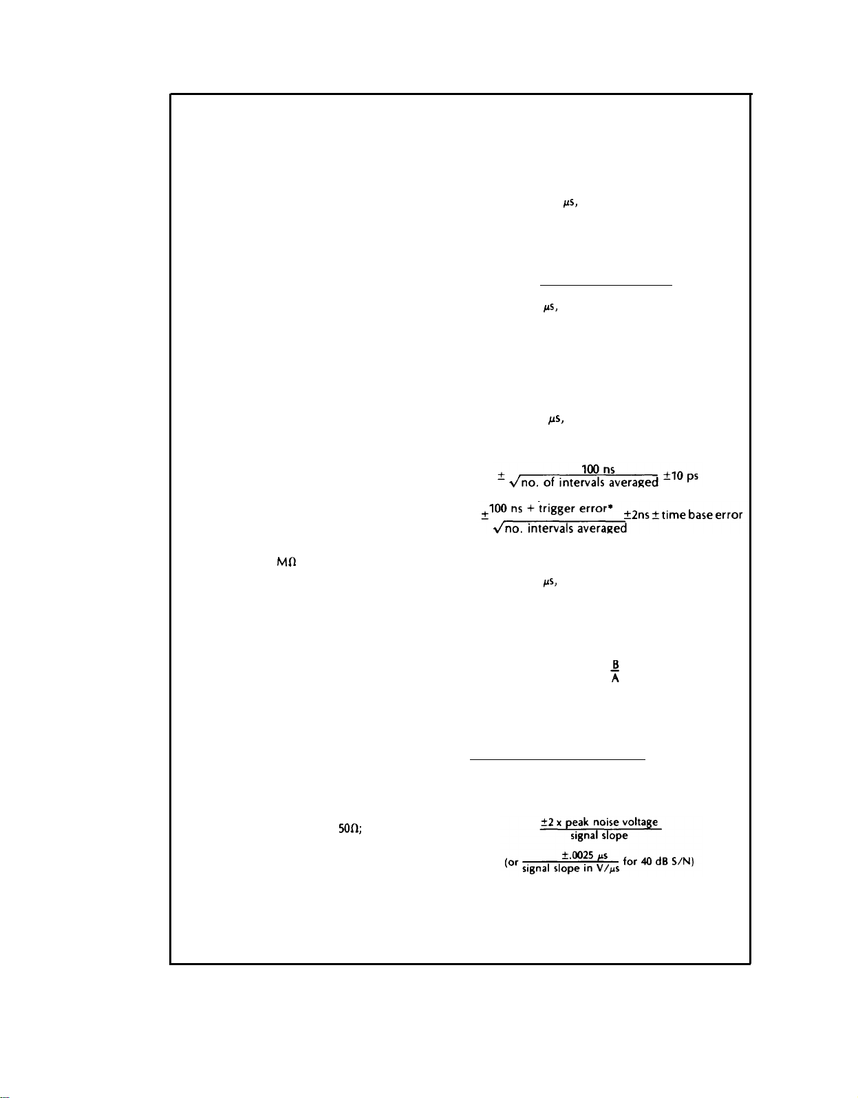
Table 1-3. 5328A Counter Specifications
Model 5328A
General Information
Power Requirements:
400 Hz ac.
Display:
Sample Rate:
seconds to HOLD.
Arming:
Refer to operation for details.
Blanking:
significant-digit are suppressed.
Hold:
HOLDS count between samples.
Trigger Light:
level.
PROGRAMMABLE OPERATION
Includes independent selection of coupling,
trigger slope, trigger level, and attenuator for
each channel. Separate/Common A switch is
programmable. Also, an invert feature switches
Channels A and B; useful in all functions except
Ratio B/A.
Trigger level is programmable in 10 mV steps
in X1; 100 mV in X10; IV in X100.
Trigger level accuracy under remote control:
X1:
±35 mV
X10:
±350 mV +2% of trigger level
X100:
±3.5V +2% of trigger level
Input Characteristics
Sensitivity:
20 Hz—35 MHz (ac coupled)
50 mV rms, 35 MHz—100 MHz
Minimum pulse width 5 ns, 140 mV p-p.
Coupling:
Impedance: 1 MO
Trigger Level:
attenuator setting with 0 volt preset position.
Trigger Slope:
- slope.
Attenuators:
Dynamic Range:
attenuator setting, 0—35 MHz; 50 mV rms
times attenuator setting, 35 MHz to 100 MHz
Maximum Input:
dc coupled, X1:
1.25 x 10⁷V rms/freq., 50 kHz—2.5 MHz
5V rms, 2.5 MHz—100 MHz.
dc coupled, X10 and X100:
MHz 1.25 x 10⁹V rms/freq., 5—100 MHz
ac coupled:
0-20 Hz; same as dc coupled above 20 Hz.
Channel Input:
Marker Outputs:
trigger outputs available on front panel;
0 to 300 mV levels into
Frequency Measurements
Frequency A
Range:
Resolution:
Accuracy:
Display: Hz, kHz, MHz.
GENERAL
Nine-digit LED.
Variable from less than 2 milli-
Rear panel ARM (ON-OFF) switch.
Unwanted zeros to left of most-
Indicates input is above trigger
(CHANNELS A AND B)
15 mV rms, 0—35 MHz (decoupled
ac or dc switch selectable.
X1, X10, X100.
0—100 MHz direct count.
1 MHz to 0.1 Hz in decade steps.
±1 count ± time base error.
115 or 230 volts 60 or
II <70 pF.
Variable over ±2.5 volts times
Independent selection of + or
25 mV to 1V rms times
250V rms, dc — SO kHz
250V rms, dc 5
200V (peak ac + dc),
Separate or Common A.
A and B channel Schmidt
50Q;
<20 ns delay.
Period Measurements
Time Interval Measurements
Ratio Measurement
Period A
Range:
Resolution:
Accuracy:
Display:
Period Average A
Range:
Resolution:
Accuracy:
error
Display:
Time Interval A to B
Range:
Resolution:
Accuracy:
Display:
Time Interval Average A to B
Range:
Resolution:
Accuracy:
Minimum Dead Time:
Maximum Repetition Rate:
Display:
Ratio B/A, or C/A
Range:
Range:
Range:
Resolution:
Accuracy: ±1 count of B or C ± trigger
* Trigger error is <0.3% of one period for sine waves
of 40 dB S/N or better and amplitude equal to
sensitivity of counter. For any wave shape, trigger
error is than then:
0—10 MHz
10 ns to 0.1s in decade steps.
±trigger error*
steps.
± trigger error*
STOP to next START
error* of A times frequency of B or C (N>1)
For N=1, add 12 ns times frequency of
B or C.
±1 count ± time base error
ns,
ps,
ms.
0—10 MHz
100 ns—.01 ps in decade steps.
±1 count displayed ± time base
trigger error*
±
no. of periods averaged
Ps,
ns
100 ns to 108 seconds
100 ns to 1-second in decade
±1 count ± time base error
ps,
ms, s.
0.1 ns to 10 seconds
150 ns from one
Ps,
ns.
A: 0—10 MHz
B: 0—100 MHz
C: 30—500 MHz
1 part in ~ x N
10 MHz.
1-3
Page 19

Model 5328A
General Information
Table 7-3. 5328A Counter Specifications (Continued)
CHANNEL C
Input Characteristics
Range:
Sensitivity:
Trigger level:
Impedance:
Maximum Input:
Input protection:
overload Indicator:
Resolution:
Accuracy:
Display: Hz, kHz, MHz
30 MHz to 500 MHz direct count
15 mV rms, 30 MHz—500 MHz
0 volts
50fl
nominal
5 volts rms
from front panel. protected to 200 volts peak.
of potential overload conditions.
Input BNC fused; accessible
flashing indicator warns
1 MHz to 0.1 Hz in decade steps
±1 count ± time base error
TIME BASE
Outputs:
Output level:
External Input:
Oscillator Aging Rate:
1 MHz and 10 MHz available at rear
panel BNC in standby and operate modes
1 volts rms into
Operates from 1, 2.5, 5, and 10
MHz inputs at 1V rms.
Input impedance 1
Counter automatically switches to
external mode when external input is
present.
24-hour warmup. Oscillator oven is
energized when power cable is connected
to line voltage.
50f)
K~l<30
pF
<5x10¹⁰/day after
1-4
Page 20

Model 5328A
Installation
SECTION II
INSTALLATION
2-1. INTRODUCTION
2-2. This section provides instructions for unpacking, inspection, preparation for use, shipment, and storage.
2-3. UNPACKING AND INSPECTION
2-4. If the shipping carton is damaged, inspect the counter for visible damage (scratches,
dents, etc.). If the counter is damaged, notify the carrier and the nearest Hewlett-Packard
Sales and Service Office immediately (offices are listed at the back of this manual). Keep the ship-
ping carton and packing material for the carrier’s inspection.
2-5. PREPARATION FOR USE
CAUTION
Before connecting this instrument to an ac power line, be sure that
the 115—230-volt line selector switch on the rear panel is set to the
proper position and proper line fuse is installed (see below).
2-6. Power Requirements
2-7. This instrument can be operated on single phase 115 or 230 (-10%. +5%) volts ac. Power
required is approximately 100 VA maximum. To avoid instrument damage, the rear panel line
selector switch must be set to the correct position and the correct fuse (as labeled on the rear
panel) must be installed. See Section
III for rear panel features photograph. When shipped, the
switch is set to 115-volt ac operation.
2-8. Fuse Replacement and Installation
2-9. Two fuses are supplied with the instrument. The instrument is shipped with a 2.0 ampere
fuse installed for 115- volt operation. To change the instrument for 230-volt operation disconnect the ac power cable, set the line selector switch and install the 1.0 ampere fuse.
2-10. Power Cables
WARNING
TO PROTECT OPERATING AND SERVICING PERSONNEL, THIS
INSTRUMENT IS EQUIPPED WITH A THREE-PIN POWER RECEP-
TACLE. THE CENTER PIN OF THE RECEPTACLE CONNECTS THE
INSTRUMENT CHASSIS AND PANELS TO EARTH GROUND WHEN
USED WITH A PROPERLY WIRED THREE CONDUCTOR OUTLET
AND POWER CABLE. IMPROPERLY GROUNDED EQUIPMENT CAN
RESULT IN HAZARDOUS POTENTIALS BETWEEN EQUIPMENTS.
2-1
Page 21

Model 5328A
Installation
2-11. To accommodate the different power receptacles used throughout the world, this instrument is supplied with one of the power cables shown in Figure 2-7. The cable supplied for use
in the United States meets the specifications established by the International Electrotechnical
Commission (lEC). The male connector of this cable is a NEMA type and the female connector
is a C.E.E. type.
2-12. Connect the power cable to a power source receptacle that has a grounded third con-
ductor. If the line power receptacle is a two-pin type instead of a three-pin receptacle, use a
two- to three-pin adapter (HP Part No. 1251-0048 for USA applications) and connect the green
lead on the adapter to earth ground. See warning above. If counter is to be operated with 230V ac
line power, an Underwriters Laboratories listed connector should be used to connect power.
2-13. Operating Environment
2-14. Maximum and minimum allowable operating temperatures are listed in Table 1-3. If
these limits are exceeded at the installation site, auxiliary cooling or heating should be used to
keep the environment within limits. A l-inch space above the counter should be clear to allow
cooling air circulation. The cooling fan exhaust port at rear is to be kept clear.
2-15. Bench Operation
2-16. The instrument cabinet has plastic feet and the large tilt carrying handle will fold under
for convenient bench operation. The tilt handle permits inclining the instrument for ease in
using front-panel controls and indicators.
NOTE
The tilt carrying handle may be secured in any position by tightening
the knurled side screws.
2-17. Rack Mounting
2-18. The counter is ready for bench operation as shipped from the factory. To mount the
counter in a rack, it is necessary to order and install the rack flange kit listed in Table 7-2.
CAUTION
Ambient temperature in rack during operation should not exceed 112°F
(50°C). Be sure instrument position in rack permits adequate air circulation and that nearby equipment does not discharge hot air directly on
the instrument.
2-19. PACKAGING FOR RESHIPMENT
2-20. Original Packaging
2-21. The same containers and materials used in factory packaging can be obtained through
the Hewlett-Packard Sales and Service Offices listed at the rear of this manual.
2-22. If the counter is being returned to Hewlett-Packard for service, attach a tag indicating
the type of service required, return address, model number, and full serial number. Mark the
container FRAGILE to assure careful handling.
2-2
2-23. In any correspondence refer to the counter by model number and full serial number.
Page 22

Model 5328A
Installation
2-24. Other Packaging Methods
2-25. If factory packaging is not available, good commercial packing should be used. Contract
packaging companies in many cities can provide dependable custom packaging on short notice.
The following general instructions should be followed when repackaging with commercially
available materials.
a.
If shipping to a Hewlett-Packard Service Office or Service Center, attach a tag indi-
cating the type of service required, return address, model number, and full serial number.
b. Wrap the counter in heavy paper or plastic.
c.
Use a strong shipping container. A double-wall carton made of 350-pound test material
is normally adequate for shipments inside the U.S.
d. Use enough shock-absorbing material (3-to 4-inch layer) around all sides of the counter
to provide a firm cushion and prevent movement inside the container. Protect the con-
trol panel with cardboard.
e.
Seal the shipping container securely.
2-26. STORAGE
2-27. If the counter is to be stored for an extended period of time, it should be enclosed in a
clean, dry, sealed container. See specifications in Section I for storage environmental limitations.
2-3
Page 23

Page 24

Model 5328A
SECTION Ill
OPERATION
(OPERATORS INSTRUCTIONS)
3-1. INTRODUCTION
3-2. This section contains information necessary to understand how to control and use the
counter. Specific details and examples are provided for making measurements of frequency,
period, period average, time interval and time interval average, and ratio. How to use the external frequency standard input is described. Programming information for use with the HP-IB
Interface and the Programmable Input Module is provided. Front and rear panel controls, connectors, and indicators are described.
3-3. FREQUENCY MEASUREMENTS
3-4. To make a frequency measurement on a CW signal below 100 MHz, select FREQ A function, select the appropriate input signal conditioning, and apply the signal to A input. The
RESOLUTION switch determines the resolution of the measurement. Since the 5328A is a conventional counter, 1 Hz resolution is obtained in 1-second of measurement time (e.g., .1Hz
10 seconds). The .1 Hz best case frequency resolution limits the low frequency measurement
accuracy. In practice, low frequencies are measured by making a period or period average
measurement and inverting the result to obtain frequency.
Operation
3-5. To make a frequency measurement on a CW signal in the range of 30 to 500 MHz, select
FREQ C function and apply the signal to the Channel C input. Make sure that the amplitude
does not exceed 5V rms. The trigger level for the Channel C is fixed at 0V dc. If pulse waveforms are being measured, they must cross through 0 volts dc by at least 25 mV. Pulse widths
down to 1 ns can be counted.
CAUTION
DO NOT exceed 5 volts rms at “C” channel input. Circuits in this
channel may be damaged by higher voltages.
3-6. The A, B, and C input modules are direct count modules. Direct count allows greater resolution per-second of measurement time than prescaling techniques and is important in making
frequency measurements on pulse bursts since the allowable measurement time is fixed (it
must be less than the width of the burst).
3-7. When the 5328A is in FREQ A or FREQ C function and the rear panel ARM switch is OFF,
a measurement cycle is initiated (i.e., arms the counter) upon the first trigger level crossing at
the A (or C) input. This means that pulsed signals are measured as easily as CW if the measurement time (determined by the RESOLUTION switch) is less than the width of the pulse.
3-8. With the ARM switch ON, FREQ A and FREQ C are armed by a trigger event at the B input. This mode is useful whenever it is desired to have real time control over when a measurement is to begin. Useful applications include measuring frequency variations along a frequency
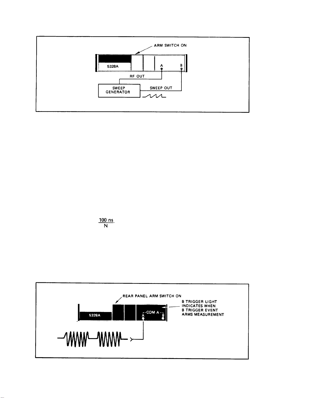
burst and linearity testing of sweep generators. Figure 3-7 illustrates the setup for measuring
the linearity of a sweep generator. The Channel B Trigger level is adjusted to trigger (and thereby arm the counter) at various points along the sweep out waveform. By plotting the B trigger
levels and the corresponding frequency measurements made at those levels, the linearity of the
generator may be determined.
3-1
Page 25
Model 5328A
Operation
3-9. PERIOD MEASUREMENTS
3-10. The PERIOD and PERIOD AVG functions allow single period measurement or multiple
period averages to be made on input signals into Channel A for frequencies up to 10 MHz. These
modes are useful for making low frequency measurements where maximum resolution is
desired.
Figure 3-1. Measuring Linearity
3-11. To make a PERIOD or PERIOD AVG measurement, select the desired function, select
appropriate input signal conditioning, and apply the signal to the A input. For single period
measurements, the RESOLUTION switch scales the time base frequency which determines the
resolution of the measurement. For optimum resolution, select N=1. Other N values may be
desirable to prevent display overflow or to get rid of unstable digits. For PERIOD AVG measurements, the RESOLUTION switch selects the number of periods over which the period average
measurement is made (the time base is 10 MHz for this case). the PERIOD AVG mode gives
increased resolution and accuracy. Trigger error is decreased by N and the resolution is in-
creased by N (resolution =
3-12. In PERIOD and PERIOD AVG with the rear panel ARM switch OFF, the measurement
cycle is initiated by the SAMPLE RATE control and the input signal. With the ARM switch ON,
PERIOD and PERIOD AVG are armed by a trigger event at the B input. To measure the frequency of a tone burst signal, use arming and the PERIOD AVG (for increased resolution over
a low frequency measurement) as shown in Figure 3-2. Select N equal to or less than the
number of periods in the tone burst and adjust Channel B trigger level to trigger on the first
cycle of the input signal.
~.
The measurement time is equal to the period times N.
3-2
Figure 3-2. Tone Burst Measurement
Page 26
Model 5328A
Operation
3-13. TIME INTERVAL MEASUREMENTS
3-14. One of two time interval functions can be selected, time interval or time interval average.
These functions measure the time interval between a START signal at the Channel A input and
STOP signal at the Channel B input. If both the START and the STOP signals are derived from
the same signal, place the COM A-SEP in COM A position. Separate slope and level controls
for each channel allow variable triggering on either positive or negative going slope.
3–15. In single-shot time interval measurements, Channel A opens the main gate and Channel
B closes the main gate. While the main gate is open, 10 MHz is divided by the setting of the
RESOLUTION switch and totalized by the counter. For optimum resolution, select N=1. Other N
values may be chosen to prevent display overflow (e.g., long time intervals) or to get rid of
unstable digits. In time interval average measurements, the main gate is open for the number
of time intervals selected by the RESOLUTION switch. The 5328A 10 MHz clock is totalized only
during the individual time intervals. The resolution of the measurement is improved by the
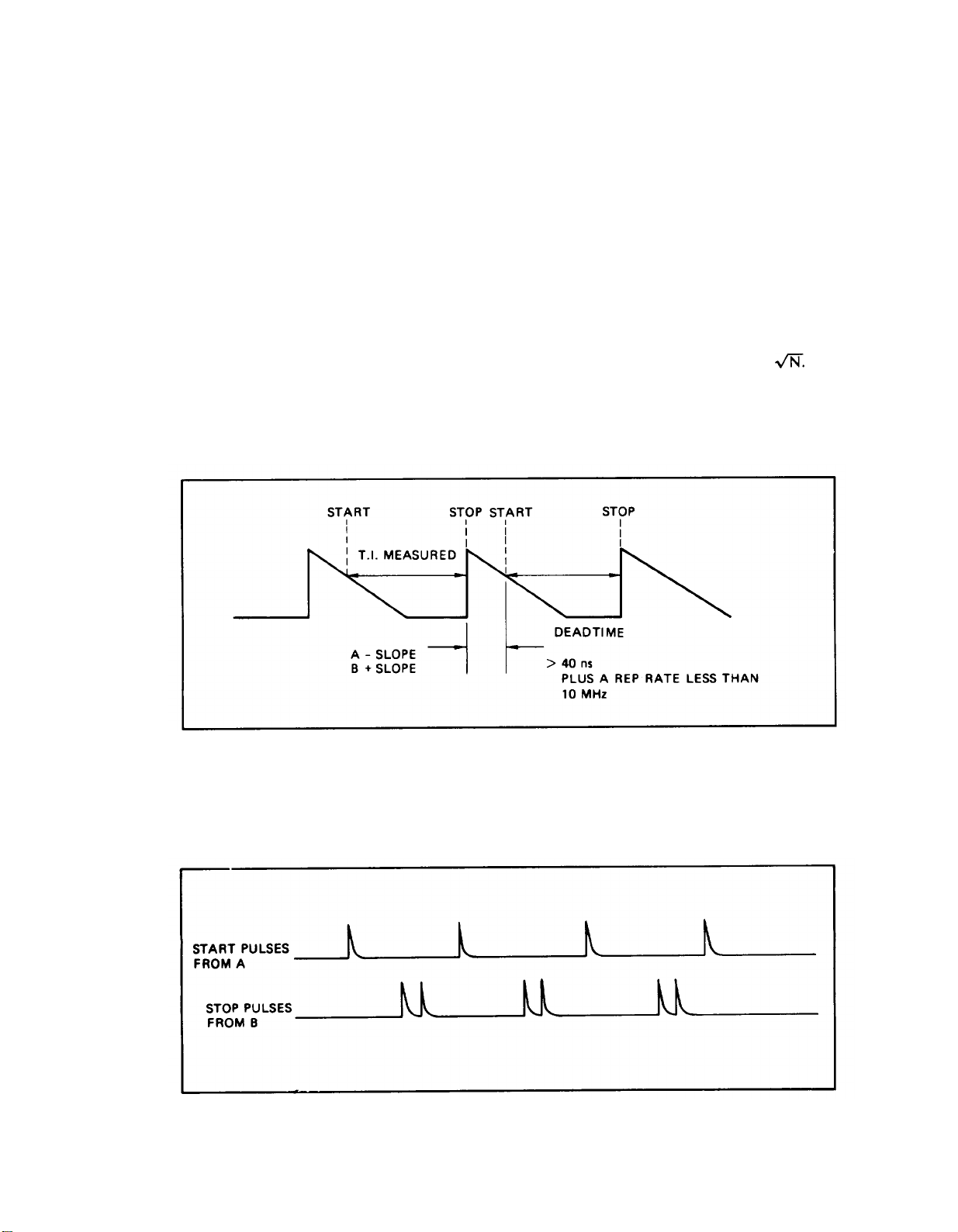
3-16. In order to allow the synchronizers time to reset during time interval averaging, there
must be at least 40 ns deadtime (and the additional constraint that the repetition rate be less
than 10 MHz). Deadtime is the time between the preceding time interval stop event and the
current time interval start event as shown in Figure 3-3.
fi.
Figure 3-3. Deadtime
3-17. During a time interval average, there must be only one stop pulse for each start pulse.
Extraneous stop pulses which occur before the next start pulse are accumulated and give erroneous readings. For example, the case illustrated in Figure 3-4 would result in a reading equal
to one-half of the desired time interval.
Figure 3-4. Multiple STOP Pukes
3-3
Page 27
Model 5328A
Operation
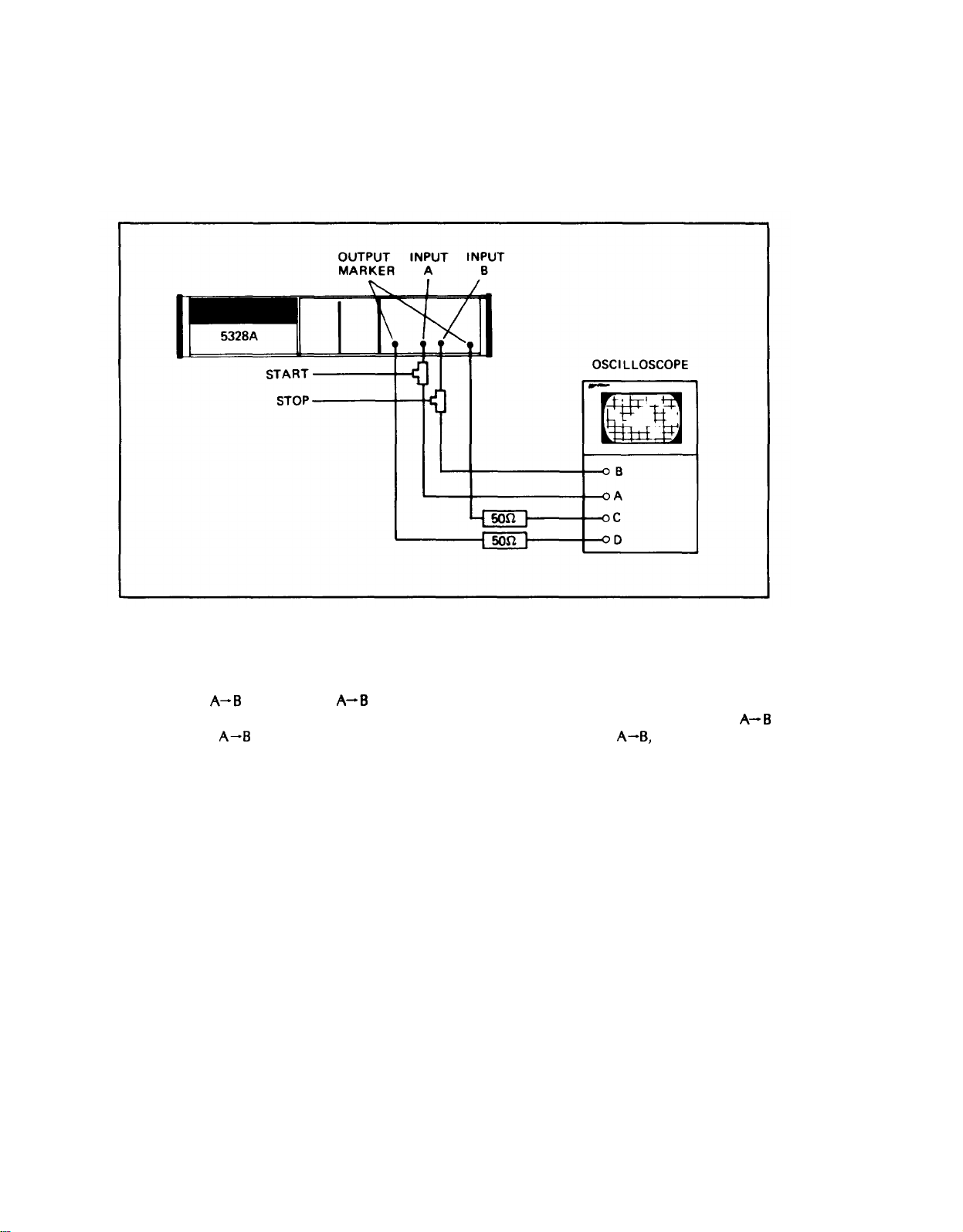
3–18. To set up a time interval measurement, the marker outputs may be monitored on an
oscilloscope (see Figure 3-5) to indicate where the channels are triggering with relation to the time
interval of interest. The GATE/MARKER OUT is high during the time interval being measured.
Figure 3-5. Monitoring Marker Outputs
A-B
3–19. In T.I.
by the run down of the SAMPLE RATE control. With the rear panel ARM switch ON, T.I.
and T.I. AVG
signal is required per average measurement (i.e., the counter doesn’t need to be armed prior
to each individual time interval in the time interval measurement).
3-20. RATIO MEASUREMENTS
3-21. For ratio measurements, the 5328A has wide bandwidth, good sensitivity, and complete
signal conditioning of the Channel A, B, and C input amplifiers.
3–22. Two ratio functions are available: B/A and C/A. The ratio of the frequency at B (or C)
to the frequency at A is measured for N counts of A where N is selected by the RESOLUTION
switch. The resolution of the measurement improves with increasing N and is given by 1 part
in B/A x N (or C/A x N). Since the range of A is 0-10 MHz while B is 0-100 MHz, the lower
frequency is normally applied to the A input although there is no restriction that this be the
case (i.e., ratios less than 1 may be measured). If B/A is greater than 1, the measurement reso-
lution is better than switching the inputs for a ratio <1, provided the value of N remains the same.
3-23. OPERATING CONTROLS
and T.I. AVG
A-B
are armed by an event at the C input. For T.I. AVG
A-B
with the rear panel ARM switch OFF, the counter is armed
A-B,
only one arming
A-B
3-4
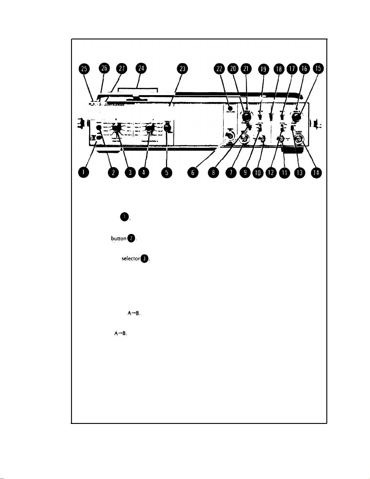
3–24. All of the front and rear panel operating controls are shown and described in Figures
3-6 and 3-7.
Page 28
Model 5328A
Operation
1.
LINE switch0.In STBY position with light on, supplies power to oven of the high stability
time base to maintain a constant temperature for the crystal. In OPER position, supplies normal
operating power to the instrument.
2.
RESET
lights all segments of the LED display and all annunciator LED’s for LED test. Returns 5328A
to LOCAL CONTROL when HP-IB Interface is in use.
3.
FUNCTION
a.
b.
c.
d.
e.
f.
g.
h.
i.
j.
button~.
FREQ A. Sets counter to measure frequency at Channel A.
FREQ C. Sets counter to measure the frequency of the signal at the Channel C input.
PER A. Sets counter to measure period at Channel A.
PER AVG A. Sets counter to make a period average measurement of the signal at Chan-
nel A. The number of periods over which the average measurement is made is determined by N, selected by the RESOLUTION switch.
T.I. AVG
interval from A to B. The number of time intervals over which the average measurement
is made is determined by N, selected by the RESOLUTION switch.
T.I.
A-B.
Channel A and the stop signal is applied to Channel B.
CHECK. Applies 10 MHz to decade counting assemblies. Verifies operation of SAMPLE
RATE control, RESOLUTION switch, and RESET.
RATIO C/A. Sets counter to measure the ratio of the signal frequency at Channel C to
the signal frequency at Channel A.
RATlO B/A. Sets counter to measure the ratio of the frequency at Channel B to the fre-
quency at Channel A.
Top blank position has no function.
Resets display and internal count to zero. When continuously depressed,
selector~.
A-B.
Sets counter to make a time interval measurement. Start signal is applied to
Selects mode of operation.
Sets counter to make a time interval average measurement of the time
Figure 3-6. 5328A Front Panel Operation Summary
3-5
Page 29
Model 5328A
Operation
3-6
Figure 3-6. 5328A Front Panel Operation Summary (Continued)
Page 30
Model 5328A
Operation
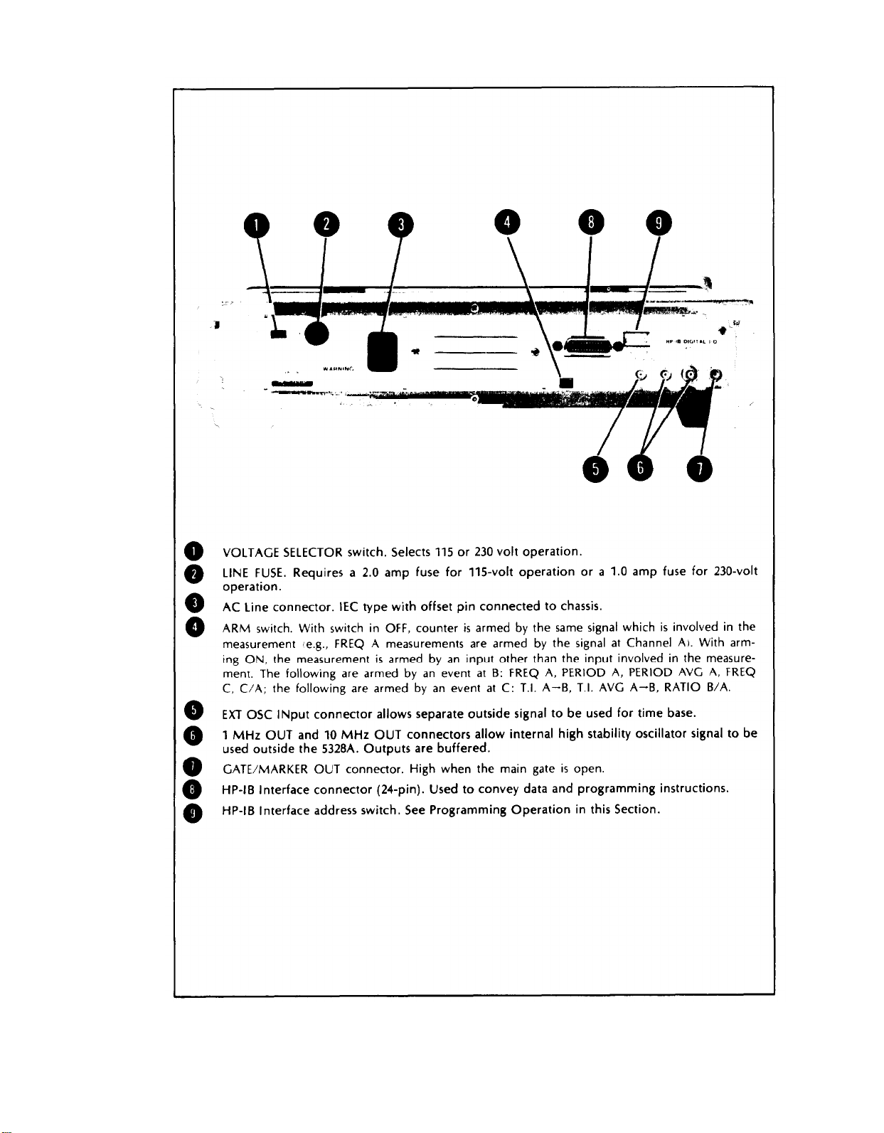
Figure 3-7. 5328A Rear Panel Controls and Connectors
3-7
Page 31

Model 5328A
Operation
3-25. FUNCTION OF CONTROLS, INDICATORS, INPUTS, AND OUTPUTS
3-26. The following paragraphs provide a detailed description of the function of controls, indi-
cators, and connectors.
3-27. Display
3-28. The 5328A counter display consists of nine-digit, seven-segment LED display and annun-
ciators for indicating the measurement units of Hz, s, as well as multiplier indicators (K, m,
n). These display units and multipliers are automatically displayed along with the correct decimal point location. Overflow (OVFL) indicates that left-most-significant digits have overflowed
the display. Remote (RMT) indicates that the counter (HP-IB interface) is under remote program
control. A GATE lamp indicates that the counter has been armed and that a measurement is
in process.
3-29. Power (Line)
3-30. The LINE switch puts the counter in OPER (operate) or STBY (standby). The STBY
position with STBY light on turns off some but not all the power supply voltages. This circuit
arrangement allows the high stability oscillator to operate continuously. Therfore, the input
to main power transformer (T1) plus the unregulated dc voltage to the oscillator oven is always
energized whenever power is connected even with the line switch in STBY.
~,
3-31. Reset
3–32. The RESET pushbutton resets the display and internal count to zero and also initiates
single measurements when the SAMPLE RATE control is in the HOLD mode, The HP-IB interface,
provides remote control capability, pushing the RESET button restores the counter to local control (when not remotely locked out by the HP-IB Local Lockout universal command). Refer to
programming in this section.
3-33. Sample Rate Control
3–34. The SAMPLE RATE control sets the minimum time between samples, The time is con-
tinuously variable from less than 2 milliseconds between measurements to HOLD, which holds
the display indefinitely.
NOTE
The counter will internally (self) arm (via the SAMPLE RATE control)
only when ARMing is OFF and the FUNCTION selected is at other
than FREQ A, FREQ C, and RATlO C/A.
3-35. Arming
3-36. The counter may be armed internally (i.e., made ready to start a measurement) by the
SAMPLE RATE control, or externally by the input signal itself, (arming off) or by a signal not
directly involved in the measurement (arming on). Table 3-7 is an arming status table. A rear
ps
panel switch turns ARMing either ON or OFF. The counter is armed within 1
ps
at the B arming input and is armed within 10
after the event of the C arming input.
after the event
3-8
Page 32

Model 5328A
Table 3-1. Arming Status
3-37. Frequency Resolution, N Switch
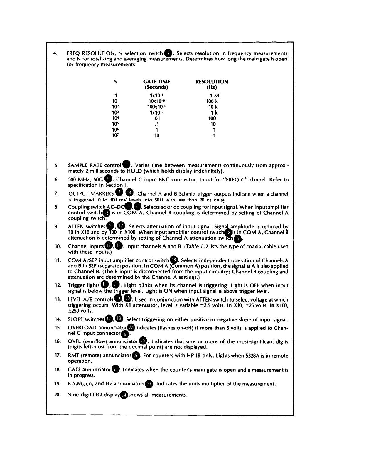
3-38. The FREQUENCY RESOLUTION, N switch determines the amount of time that the
counter’s main gate is open for a particular measurement when the Main Gate FF (refer to
Section IV) determines the gate time. Depending on the measurement, this time results in a
certain measurement resolution (e.g., frequency measurements), a number of intervals averaged (e.g., T.1. AVG measurements), or a scaling factor by which the time base is divided (e. g.,
period measurements). Table 3-2 shows the setting of the RESOLUTION switch and the corresponding time the main gate is open.
Operation
Table 3-2. Frequency Resolution, N Switch Settings and Gate Times
3-39. Table 3-3 summarizes the FUNCTIONS
FREQUENCY RESOLUTION, N switch setting.
Table 3-3. Functions and Resolution Switch Settings
and the corresponding interpretation of the
3-9
Page 33

Model 5328A
Operation
3-40. Input Channel Section
3-41. Two separate inputs are provided on the right side of the panel. The A and B inputs are
identical in specification and identical controls are provided for each input to allow maximum
versatility and accuracy.
3-42. HP-IB PROGRAMMABLE INPUT CONTROLS. In COM A position, the output of the
Channel B attenutor is disconnected. The output of the Channel A attenuator is routed to the A
and B input amplifiers as shown in Figure 3-8. In COM A the Channel B AC-DC, X1, X10, X100
Attenuator relays are disabled. The Channel A AC-DC, X1, X10, X100 Attenuator determine the
coupling for the Channel B amplifier.
3-10
Figure 3-8. Programmable Input Switch Configuration for COM A
3-43. The A and B input amplifiers have independent LEVEL and SLOPE controls regardless
of the mode of operation (SEP or COM A).
3-44. A and B Channel Signal Conditioning
3-45. AC-DC SWITCH. The AC-DC switch controls the coupling of the external signal to the
attenuator-amplifier by switching a capacitor in series in the AC position or by direct coupling
in the DC position. The advantage of AC coupling is to provide a DC block for signals with a
DC component. DC has the disadvantage of being unable to pass low frequency signals. A
distinct advantage of having DC coupling cover the full bandwidth (DC-100 MHz) is that
extremely accurate time interval or pulse measurements can be achieved even though pulse
widths or repetition rates vary since the trigger point is independent of the duty cycle of the input
signal.
3-46. ATTENUATOR. The attenuator (ATTEN) connects the input signal directly to the
amplifier (in X1) or through a 10:1 attenuator (X10) or a 100:1 attenuator (X100) to increase the
voltage range by 10 or 100 times to allow measurement of high level signals that would otherwise be impossible without external attenuation.
Page 34

Model 5328A
Operation
3-47. SLOPE SWITCH. The ±SLOPE switch (provided for each channel) determines which slope
of the input signal will trigger the counter. As a simple example, (Figure 3-9) if the pulse width of a
positive pulse is to be measured, the A channel slope switch would be set to “+” and the B channel would be set to “-” (for time interval measurements the A channel always begins the measurement and the B channel ends the measurement).
NOTE
A simple pulse width measurement is achieved with the use of the
+SLOPE setting for Channel A and the -SLOPE setting for Channel B.
Figure 3–9. Slope Switch Settings
3-48. LEVEL CONTROL. The LEVEL control for each channel is adjustable over the range of
±2.5V dc with the attenuator for that channel in the X1 position. A typical use of the LEVEL controls is shown in Figure 3-10.
NOTE
Simple measurement of a time interval, the LEVEL control of the A
and B input channels were used to set the trigger LEVEL of A and B.
Figure 3-10. Level Control Settings
3-11
Page 35

Model 5328A
Operation
3-49. Channel C Input
3-50. The CHANNEL C 500 MHz
A and B input channel range (0 to 100 MHz).
3-51. “C” Channel Overload lndicator
3-52. The OVERLOAD (CHANNEL C) indicator will flash on and off if the voltage maximum
is exceeded at the “C” channel input.
3-53. Hysteresis Band of Trigger Levels
3-54. The width of the trigger level hysteresis band, shown in Figure 3-77 is determined by the
sensitivity of the counter. For frequencies below 40 MHz, it is typically less than 25 mV peak-topeak. At frequencies from 40 MHz to 100 MHz, it is typically less than 70 MHz peak-to-peak. The
signal must pass through the entire hysteresis band before a trigger pulse is generated. If the
SLOPE switch is set to “+”, the trigger pulse occurs at the top of the hysteresis band. If the SLOPE
switch is set to “-”, the trigger pulse “occurs at the bottom” of the hysteresis band.
500
input is useful for higher frequency signals out of the
CAUTION
The “C” channel input signal should be limited to 5 volts maximum.
If this limit is exceeded the inline fuse may open (blow).
3-12
Figure 3–11 Hysteresis Band
3-55. Since trigger level measurements indicate the center of the hysteresis band, a better
value for the actual trigger level may be obtained by subtracting one-half the hysteresis band
(“-” slope) or adding one-half the hysteresis band (“+” slope). A typical value for the width of
the hysteresis band is 30 mv peak-to-peak.
3-56 The value to use for the hysteresis band depends on the frequency; or, for pulses, it de-
pends on the rise time.
3-57. External Frequency Standard Input
3-58. The rear panel external frequency standard (EXT OSC IN) input is useful for locking
the counter to a high stability external frequency standard. This external standard must be 1,
2.5,5, or 10 MHz, with an amplitude of >1V rms into 1
kfl
(maximum input of 5 volts peak-to-peak).
Page 36

Model 5320A
Operation
3-59. Marker Outputs
3-60. Two marker output connectors are mounted on the front panel. These outputs represent
the Channel A and Channel B Schmitt triggers. The outputs provide 0 to 300 mV levels into
50Q
delayed by less than 20 ns. These outputs are useful for oscilloscope monitoring, Time
interval measurement setups are simplified if the time interval of interest and the marker outputs can be simultaneously displayed on oscilloscope traces. Frequency measurements on noisy
signals can be made with more confidence since the markers can indicate the presence of noise
triggering. These outputs are protected from inadvertently applied voltage to ±5V dc.
3-61. Gate/Maker Out
3-62. the GATE/MARKER OUT rear panel connector supplies a TTL level which is high when
the counter’s main gate is open and low when it is closed. Monitoring the GATE OUT on an
oscilloscope can provide this information for applications where the markers do not give the
desired information.
3-63. 1 MHz and 10 MHz Frequency Standard Outputs
3-64. The 1 MHz OUT and 10 MHz OUT connectors are on the rear panel. When terminated
in 50 ohms, the output is a square wave of approximately l-volt amplitude.
3-65. Trigger Lights
3-66. A trigger light is provided for each (A and B) input channel to enable the user to know
not only if the channel is triggering, but also in which direction the trigger level must be ad-
justed to cause triggering. The light is ON when input is above the trigger level; OFF when in-
put is below the trigger level; BLINKING when channel is triggering. The trigger lights are
operative over the full frequency range of dc to 100 MHz.
3-67. The trigger lights can be used with a 10:1 oscilloscope probe to provide a logic probe
function. By adjusting the trigger level to one-tenth (since using 10:1 divider probes) of the
threshold voltage for the logic family under investigation (e.g., .14 volts for TTL), the light indicates the logic state of circuit points which are contacted with the probe. When the trigger
level light is ON, the circuit node is a high (i.e., above the threshold voltage). If the light is OFF,
the node is a logical low. If the light blinks, then pulses (up to 100 MHz rep rate) are present at
the node. The trigger lights can also detect the polarity of low rep rate pulses down to 5 ns pulse
width. Positive pulses cause the light to blink on while negative pulses cause the light to blink
off.
3-68. PROGRAMMING OPERATION
3-69. The 5328AF/096/H42 Universal Counter is fully compatible with the Hewlett-Packard
Interface Bus (HP-1B) IEEE Standard 488-1975 Appendix C.
3–70. Procedures for verification of proper operation of the 5328AF/096/H42 in the remote
mode are contained in paragraphs 5–37 through 5-42.
3-71. SETTING ADDRESS SWITCHES
3-72 To use the 5328A in an HP-IB based system the first step is to set the rear panel address
switches shown in Table 3-4. The left-most switch sets the counter to ADDRESSABLE or TALK
ONLY mode. ADDRESSABLE mode is used whenever a calculator or other controller is used
within the system. TALK ONLY mode is used when the counter will be controlled manually but
will output results to another device on the bus such as a printer or D/A converter.
3-13
Page 37

Model 5328A
Operation
3-73. The five right-hand switches, AS through A1, set the talk and listen addresses to the
5328A when it is used in the ADDRESSABLE mode. Table 3-4 shows the possible address settings
and the corresponding ASCII codes for talk and listen addresses.
Table 3-4. Addresssing
3-14
Page 38

Model 5320A
Operation
3–74. Table 3–5 gives the program code set for the 5328AF/096\H42. All Function, Frequency
Resolution, N and Channel A/B Signal Conditioning are analogous to the corresponding frontpanel operations described previously.
Table 3-5. Program Code Set
3-15
Page 39

Model 5328A
Operation
3-75. MEASUREMENT OUTPUT FORMAT
3-76. The 5328AF/096/H42 transmits the following string of characters to output a measurement:
3-77. BUS COMMANDS
3-78. The 5328AF/096/H42 obeys the following HP-1 B Universal Commands and Addressed
Commands (ASCII codes shown in
a. Universal Commands:
LLO Local Lockout (ASCII DC1)
Disables all programmable front panel controls including reset. Go To
Local (GTL) must be programmed to return to manual control.
DCL Device Clear (ASCII DC4)
Resets the programmed state of the counter to the codes shown in bold
face in the program code set. Has the same effect as the program code
“P”.
SPE Serial Poll Enable (ASCII CAN)
Sets the counter to the serial poll mode. When addressed to talk during
the serial poll mode, the 5328A produces a status byte to indicate its
condition. If the counter has completed a measurement and it requesting
service, the status byte contains a “1” in bit 7 (decimal value 64). If the
counter has not requested service, the status byte will be “0” in all bits.
When addressed to talk in the serial poll mode, the counter will
immediately stop requesting service.
SPD Serial Poll Disable (ASCII EM)
Terminates the serial poll mode. The 5328A can resume its normal data
output mode.
parenthesis and in Table 3-6).
3-16
Page 40
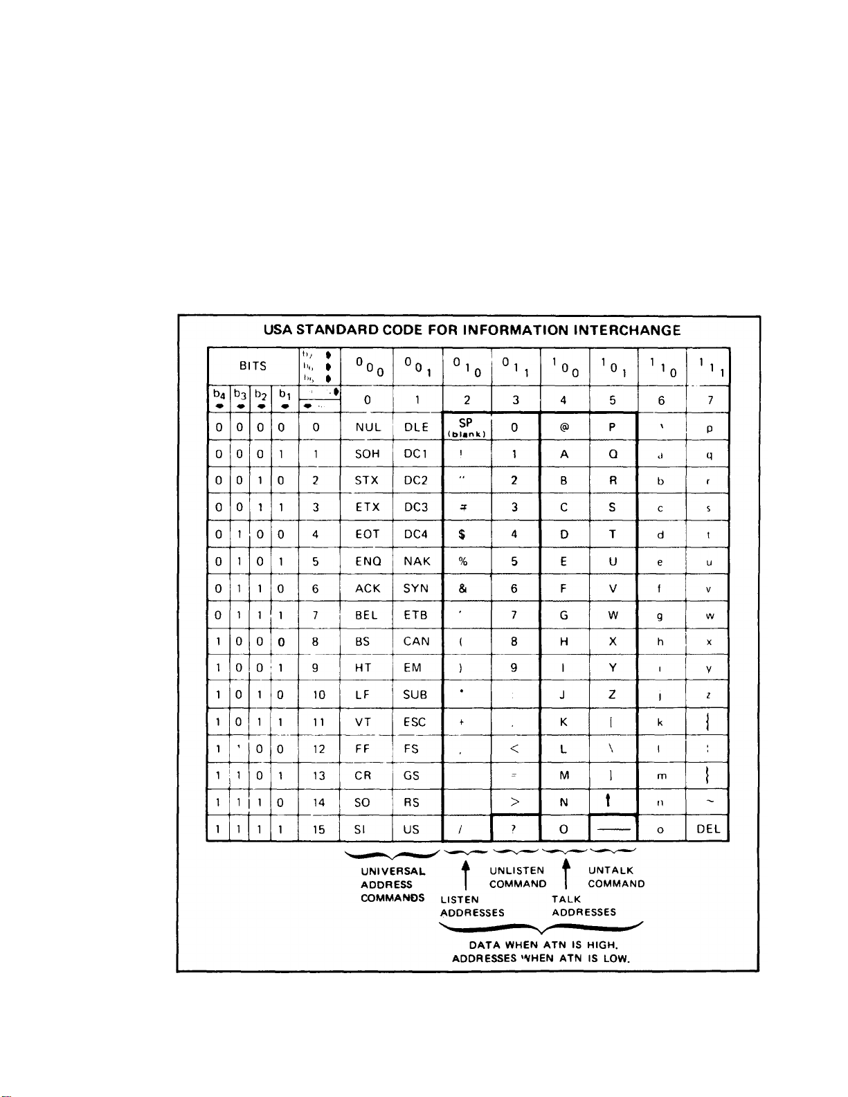
b. Addressed Commands:
GTL Go To Local (ASCII SOH)
Returns the 5328A to local (manual) control from remote control.
SDC Selected Device Clear (ASCII EOT)
Responds as with Device Clear or program code “P”.
GET Group Execute Trigger (ASCII BS)
Starts a measurement. This command provides the quickest method to
start a measurement cycle.
Table 3-6. American Standard Code for Information Interchange (ASCII)
Model 5328A
Operation
3-17
Page 41

Model 5328A
Operation
3-79. PROGRAM EXAMPLES
3-80. The following examples illustrate the programming capability of the 5328AF/096/H42,
using the HP9825A Desktop Computer as a computing controller.
3-81. Example 1
3-82. This program sets the 5328AFA/096/H42 into its CHECK mode, with 1 Hz resolution.
The program takes a measurement (trg 701) and reads it into the A register of the HP9825A.
After waiting 500 ms, the program loops back to line 1 for the next trigger.
3-18
Page 42
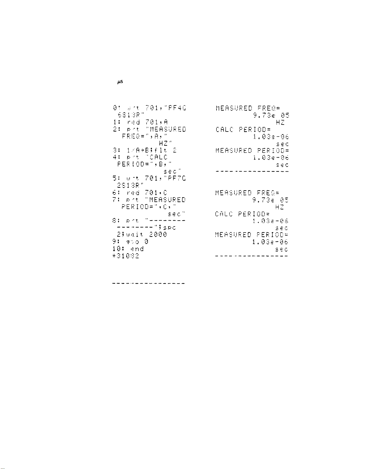
Model 5328A
Operation
3-83. Example 2
3-84. This program sets the 5328AF/096/H42 into its Frequency mode with 1Hz resolution.
The program takes a frequency measurement, reads it into the A register of the HP9825A,
and prints the results. The calculator computes the period from the frequency measurement
and prints the calculated period. The program then sets the 5328AF/096/H42 into its PERIOD
+
mode with 10
HP9825A and printed. After waiting 2 sec, the program loops back to line 0 for the next trigger.
resolution. A period measurement is made, read into the C register of the
3-19
Page 43

Page 44

Model 5328A
Theory of Operation
SECTION IV
THEORY OF OPERATION
4-1. INTRODUCTION
4-2. This section contains a description of the operating principles of the counter in reference
to an overall block diagram in this section and to individual block and schematic diagrams in
Section Vlll.
4-3. OVERALL DESCRIPTION
4-4. The 5328A is a 500 MHz universal frequency counter with the following capabilities.
Frequency —
Period —
Period Average — 10 MHz clock
Time Interval — 100 ns single-shot resolution
Time Interval Average
Ratio —
Check
4-5.
4-6. The operation of the frequency counter is best understood by describing how the counter
performs a frequency measurement. If n is the number of cycles of a signal that occurs in a time
period, t, the average frequency, f, of that signal over the time period, t, is given by
4-7. Frequency
4-8. The counter measures the frequency, f, by accumulating the number of cycles, n, of the
input signal that occurs over the time period, t. The basic counter elements necessary to per-
form this measurement are shown in Figure 4-1.
BASIC COUNTER OPERATION
100 and 500 MHz direct count
100 ns resolution
100 MHz/10 MHz
(1)
Figure 4-1. Basic Elements of the Frequency Counter
4-1
Page 45

Model 5328A
Theory of Operation
4-9. INPUT AMPLIFIER AND TRIGGER — essentially conditions the input signal to a form
that is compatible with the internal circuitry of the counter. As Figure 4-7 indicates, the output
of the amplifier/trigger is a pulse train where each pulse corresponds to one cycle or event of the
input signal.
4-10. TIME BASE OSCILLATOR —
equation (1) is derived. From equation (1) it may be seen that the accuracy with which t is
determined has a significant effect on the measurement accuracy of the frequency, f. The 5328A
employs a 10 MHz temperature-controlled (oven-regulated) precision, crystal oscillator as the
time base element.
4-11. DECADE DIVIDERS —
an output a pulse train whose frequency is variable in decade steps. The operator can control
this frequency with the FREQ RESOLUTION, N switch. The time, t, of equation (1) is determined by the period of this pulse train.
4-12. MAIN GATE —
amplifier/trigger are allowed to pass through. The opening and closing of the main gate is controlled by the decade divider output to the main gate flip-flop.
4-13. DECADE COUNTING ASSEMBLIES —
displays this total after the gate is closed. If, for example, the gate is open for precisely 1 second,
the decade counting assemblies (DCA’s) display the frequency, in Hertz, of the input signal.
4-14. Other basic measurements the counter can perform are described in the following
paragraphs.
4-15. Period
4-16. Period, the inverse of frequency, can be measured with the counter by reversing the
inputs to the main gate. Now the input signal controls the duration over which the main gate
is open and the decade divider output is counted by the DCA’s. The duration of the count is, of
course, one cycle or period of the input signal (see Figure 4-2).
is the heart of the counter. When this gate is opened, pulses from the
is that element of the counter from which the time, t, of
take the time base oscillator signal as the input and provide as
totalizes the output pulses from the main gate and
4-17. Unused decades in the decade divider chain can be used to divide the amplifier/trigger
output so that the gate remains open for decade steps of the input period rather than a single
period. The is the basis for multiple period averaging. Period and period averaging techniques
are used to increase measurement accuracy on low frequency measurements.
Figure 4-2. Measuring Period
NOTE
The roles of the amplifer/trigger and decade divider outputs are reversed in measuring the period. This same configuration also serves
for ratio measurements with the second input replacing the time base
oscillator.
4-2
Page 46
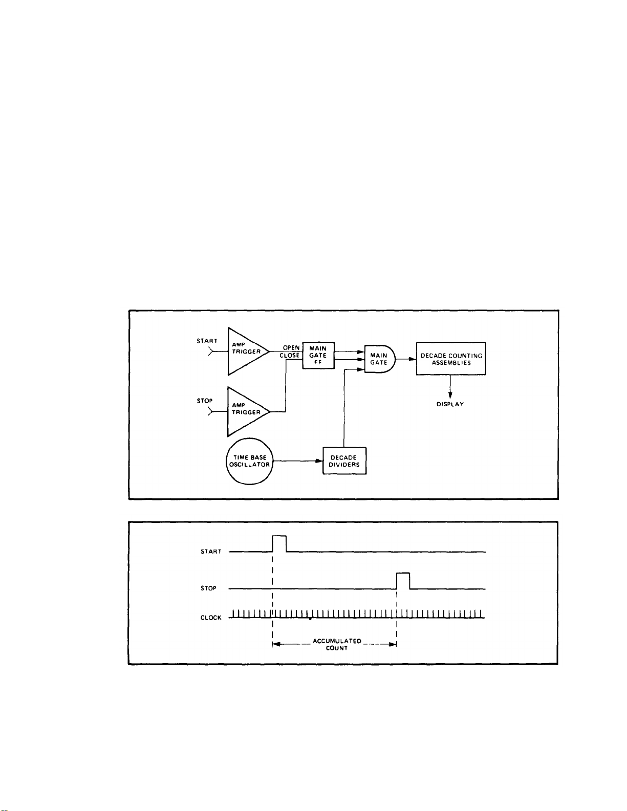
4-18. Ratio
Model 5328A
Theory of Operation
4-19. By replacing the time base with a second input of frequency, f
as in Figure 4-2 can be used to measure the ratio f
/f. For higher resolution the signal at fre-
2
; the same configuration
2
quency f can be divided in decade steps in a manner identical to multiple period averaging.
4-20. Time Interval
4-21. Figure 4-3 shows the configuration for the measurement of time between two events or
time interval. The main gate is now opened by the START input and closed by the STOP. The
decade divider output is again counted and the display shows the elapsed time between START
and STOP signals. The measurement of time interval is considered in more detail in paragraph 4-22.
4-22. TIME INTERVAL, RESOLUTION, AND AVERAGING TECHNIQUES
4-23. Time interval, the measurement of the time between two events, is shown in the block
diagram shown in Figure 4-3. The main gate is now controlled by two independent inputs, the
START input opening the gate and the STOP input closing it. Clock pulses are accumulated for
START and STOP. This is shown in Figure 4-4.
Figure 4-3. Basic Elements of a Time Interval Counter
Figure 4-4. Clock Pulses
NOTE
In a time interval measurement, clock pulses are accumulated for the
duration the main gate is open, The gate is opened by one event,
START and closed by the other, STOP.
4-3
Page 47

Model 5328A
Theory of Operation
4-24. Resolution
4-25. The resolution of the measurement is determined by the frequency of the counted clock
(e.g., a 10 MHz clock provides 100 ns resolution). The elements within the time interval counter
(input amplifier, main gate, DCA’s) must operate at speeds consistent with the clock frequency,
otherwise the instrument’s resolution would be meaningless. The 5328A counts a 10 MHz clock.
4-26. Clock frequencies of 1, 10, 100 MHz, and other 10n frequencies, are preferred since the
accumulated count, with the appropriate placement of decimal point, gives a direct readout of
time interval. This explains why the conventional time interval counter is at present limited to
10 nanoseconds, a clock frequency of 100 MHz. 1 GHz is beyond reach and a clock frequency of
200 MHz would require some arithmetic processing of the accumulated count in the DCA’s to
enable time to be displayed directly.
4-27. Time Interval Averaging
4-28. This technique is based on the fact that if the ±1 count error is truly random it can be
reduced by averaging a number of measurements. The words “truly random” are significant.
For time interval averaging to work, the time interval must (1) be repetitive, and (2) have a
repetition frequency which is a synchronous to the instrument’s clock. Under these conditions
the resolution of the measurement is:
where N = number of time intervals averaged
4-29. With averaging, resolution of a time interval measurement is limited only by the noise
inherent in the instrument. Ten picosecond resolution can be obtained with the 5328A. Most
time interval averaging suffers one severe limitation; the minimum measurable time interval
is limited to the period of the clock. This limitation is removed by circuits known as synchro-
nizers which are used in the 5328A to measure intervals as short as 100 picosecond.
4-30. The 5328A synchronizers operate as shown in Figure 4-5. The top waveshape shows a
repetitive time interval which is asynchronous to the square wave clock. When these signals are
applied to the main gate, an output similar to the third waveform results (no synchronizers).
Note that much of this output results in transitions of shorter duration than the clock pulses.
DCA’s designed to count at the clock frequency are unable to accept pulses of shorter duration
than the clock. The counts accumulated in the DCA’s will therefore approximate those shown
in the fourth trace
duration pulses actually counted by the DCA’s cannot be known. Since the time interval to be
measured is slightly greater than the clock period, the fourth waveshape shows that the average
answer will be in error, having been biased, usually low, because of the DCA’s requirement of
having a full clock pulse to be counted.
4-31. This problem is alleviated by the synchronizers which are designed to detect leading
edges of the clock pulses that occur while the gate is open. The waveshape applied to the DCA’s,
when synchronizers are used, is shown by the fifth waveform. The leading edges are detected
and reconstructed, such that the pulses applied to the DCA’s are of the same duration as the clock.
— the exact number of counts is indeterminant since the number of short
4-4
4-32. Synchronizers are a necessary part of time interval averaging; without them the averaged answered is biased. In addition, it may easily be seen that with synchronizers involved,
time intervals of much less than the period of the clock can be measured, This technique is only
as good as the synchronizers, however. The 5328A high-speed synchronizers enable intervals
as small as 100 picosecond to be measured.
Page 48

Model 5328A
Theory of Operation
Figure 4-5, Synchronizer Operation with Time Interval Averaging
4-33. There are occasional situations where time interval averaging cannot be performed on
a periodic signal. This problem occurs when the input time interval repetition rate is synchro-
nous with the internal clock.
4-34. SOURCES OF MEASUREMENT ERROR
4-35. The major sources of measurement error are the ±1 count ambiguity, the time base error
and trigger error. These are discussed in the following paragraphs.
4-36. ±1 Count Ambiguity
4-37. Since the signal input to the main gate of the counter and the clock input are not coherent,
an inherent ±1 count ambiguity exists in the count accumulated in the decade counting assem-
blies. This is illustrated by Figure 4-6.
Figure 4-6. ±1 Count Ambiguity
NOTE
The main gate is open for the same time, tm, in both cases. incoher-
ence between the clock and the input signal can result in two different
counts which for this example is one for case A and two for case B.
4-5
Page 49

Model 5328A
Theory of Operation
4-38. FREQUENCY MEASUREMENT ERROR. The error caused by the ambiguity is in absolute terms, ±1 of the accumulated count. For a frequency measurement the signal counted is
the input signal of frequency, f
4-39. PERIOD MEASUREMENT ERROR. For period measurement, the signal counted is the
internal time base clock of period t
4-40. MAIN GATE REQUIREMENTS. The ±1 count error described above assumes the main
gate itself does not contribute any error. As with any gate, however, the main gate does exhibit
propagation delays and takes finite times to both switch on and off. Any differential between the
times taken for the main gate to switch on and off show up as uncertainties in the length of time
the gate is open. This uncertainty in turn translates into a measurement error that increase the
±1 count. However, the uncertainty in the main gate of the 5328A is substantially less than the
period of the highest frequency counted, so this error is not appreciable.
. Thus the relative error is given by:
in
±1 count error, relative frequency measurement error
. Hence the relative error becomes:
c
±1 count error; relative period measurement error
(2)
(3)
4-41. Time Base Error
4-42. Any error in the time base oscillator directly translates itself into a measurement error.
Thus, if the total of all the oscillator errors amount to 1 x 10
time base in the measurement of a 10 MHz signal is 1 x 10
measurement of a 100-millisecond period, the error would be 1 x 10
-6
, the total error contributed by the
-6
x 107 = 10 Hz. Similarly, for the
-6
x 10
-1
= 1 x 10
-7
or 100
nanoseconds.
4-43. Trigger Error
4-44. Noise on the input signal will cause uncertainties in the point at whit} the Schmitt trigger switches. Provided the noise is not large enough to cause false triggering (i.e., cross both
limits of the hysteresis band which would produce more pulses out of the Schmitt trigger than
input cycles to it) no significant error is introduced in a frequency measurement.
4-45. For period measurements, however, this uncertainty produces like error in the time the
gate is open, since it is this signal that controls the gate. It can be shown that with essentially low
frequency noise and a signal-to-noise ratio of 40 dB, the resultant worst case trigger error is .32%
of the period. Thus, the trigger error in the measurement of the period of a 1 kHz signal is 3.2x
-3
-3
x 10
10
= 3.2 microseconds, worst case. For 60 dB signal-to-noise ratio, worst case error
is .032%; while for a 20 dB signal-to-noise ratio signal it is 3.2%.
4-46. For an arbitrary wave shape (but constant slew rate through the hysteresis band), the
trigger error takes on a different expression. In Figure 4-7, it is shown that for this case, the
trigger error is:
4-6
Page 50

Model 5328A
Theory of Operation
4--47. For time interval measurements, trigger error is generally negligible when compared
to the systematic error introduced by the uncertainty in the setting of trigger levels. For an uncertainty in trigger level of ±10 millivolt and a peak noise voltage of one millivolt, trigger error
is a factor of five less than the error caused by trigger level uncertainty, regardless of signal
slew rate. For example, trigger level uncertainty of ±10 millivolt on a 100 millivoIt/nanosecond
signal introduces an error in the time interval measurement of ±0.1 nanosecond. The trigger
error for such a signal, with 1 millivolt peak noise, is less than ±.02 nanosecond, a factor of five less.
Averaging reduces the trigger error still further (but not the trigger level uncertainty error). The
~N
error is reduced by
for time interval averaging and by N for period averaging.
Figure 4-7. Trigger Error
4-48. 5328A PRINCIPLES OF OPERATION
4-49. The 5328A is organized into four main operating sections (refer to Figure 4-8):
• The main counter section
Ž The input section
• The power supply section
• The Hewlett-Packard Interface Bus (HP-IB) section
4-50. Each section operates relatively independently and communicates to the other through an
internal bus system. The two-way bus consists of 90 lines.
4-51. The power supply provides regulated dc voltage for the other operating sections of the
instrument. The main on-off switch of the instrument operates only the central power supply
regulator; the main ac power line is never broken. Unregulated dc is constantly fed to the oven
oscillator eliminating the need for time base warmup. The fan is dc powered.
4-52. Main Counter Section
4-53. The main counter section on A1 Motherboard contains all of the functional subunits of
a standard counter with the exception of input signal conditioning and special logic, which are
contained in the input section. The decade counting assembly contains eight decades of BCD
counting logic, latches, and output multiplexing logic. The time base assembly contains eight
4-7
Page 51

Model 5328A
Theory of Operation
4-8
Figure 4-8. Block Diagram
Page 52

Model 5328A
Theory of Operation
counting decades, output multiplexing logic, and synchronizers to generate precise timing
signals for the main gate. The oscillator section contains the input/output logic to accept an
external signal via the rear panel or an internal signal from the oven-regulated crystal oscillator.
4-54. The sample rate circuit controls the instrument display cycle.
Inhibit, reset, main gate,
transfer, and sample rate signals are generated in this circuit, as is the BCD digit address code
for the strobed display. Generation of decimal point and annunciators and decoding of BCD
data are accomplished by the display control circuits. Data out of the decade counting assembly
or the input modules is decoded and displayed on the nine-digit LED display.
4-55. The A4 Function Selector serves as the main signal switch of the instrument. It routes
input signals through multiplexer to the decade counting assembly and/or the time base. At
the same time, it interacts with the display control circuits to determine the beginning and end
of the display cycle. The precision main gate signal is created on the function selector through
interaction with the time base assembly. The function selector also has extensive interaction
with the input modules. It is the main receiver of the high-speed data from the modules and
the originator and receiver of module arming pulses.
4–56. The flexibility of the 5328A comes from the ability of all these operating subsections to
accept diverse data from input modules. This is accomplished through the use of a 4000-bit
read-only memory (ROM) as the master control of the instrument. Located in the main counter
section of the instrument, the ROM accepts the four-bit function code and the three-bit time
base code from the front-panel switches or the HP-IB remote programming board. The ROM
generates 32 bits of output data which are transmitted throughout the instrument to set-up each
subsection for the particular measurement situation.
4-57. Input Section
4-58. The input modules are the main interface between the instrument and the outside elec-
tronic environment. They accept input signals and convert them into the proper form to be
handled by the main counter circuits.
4-59. The middle area of the input module section provides the 5328A with extended frequency capability (Channel C). A
50fl fuse-protected 500 MHz amplifier and Schmitt trigger
feed the 500 MHz decade. Latches in this section strobe the ninth (least-significant) digit from
the module onto the data bus and into the display. In functions not requiring an input from this
module, ROM lines deactivate the output strobing circuitry and the ninth digit on the display
goes blank.
4-60. Hewlett-Packard Interface Bus (HP-US) Section
4-61. The fourth section of the instrument, the HP-IB assembly provides for control of the
counter by the HP-IB. Connected to the main instrument bus through a ribbon cable, the
internally-mounted HP-IB board controls function, time base, cycle rate, arming, and other
controls in the instrument.
4-62. A1 MOTHERBOARD
4-63. The A1 Motherboard consists of five sections, as follows:
Display control.
a.
b. State control.
c. Oscillator.
d. Decade Counting Assembly.
Time Base.
e.
4-9
Page 53

Model 5328A
Theory of Operation
4-64. Display Control
4-65. The display control section on Al Motherboard acts as an interface between the A16
Display board and the other circuits of the counter.
4-66. The outputs of the A16 Display Board FUNCTION and RESOLUTION switches go to the
ROM (A1U37). The outputs of the ROM position the decimal point and annunciators in the display and provide control functions for other circuits of the counter. Data from the data bus is
translated from BCD to seven-segment form in decoder U41 and sent to the display which is
strobed by U39. U39 decodes the digit address code from BCD to one of 10 forms. Leading zero
blanking is provided by the latch comprised of U32B and U40B. Latches U25, U26, U27, and
U31 provide outputs related to function and time base codes for use in other sections of the
instrument.
4-67. State Control
4-68. The state control section is comprised of circuits U1, U2, U3, U4, and US. Decade Counter
U1 generates the digit select strobe code for the display. Circuit U4 receives the Sample Rate
signal and generates the main Reset, Transfer, and Inhibit signals.
4-69. A3 OSCILLATOR SUPPORT
4-70. An oven-temperature-regulated crystal oscillator (A3A1) supplies the precision 10 MHz
time base signal in the 5328A. The A3A1 crystal oscillator (also designated HP Model 10544A)
is in rectangular metal enclosure which plugs into the A3 Oscillator Support. The A3 Oscillator
Support in turn plugs in the A1 Motherboard.
4-71. A3 Oscillator Support
4-72. On the A3 Oscillator Support five separate functional circuits are provided: a voltage
regulator, an external signal detector, and amplifier-multiplier, a multiplexer, and a 10:1 divider.
Integrated circuit U3 is a voltage regulator which regulates the 25-volt power at about 13 volts
for the oscillator. External signal detector U4C will detect if an external signal (1, 5, or 10 MHz)
is applied to the 5328A rear panel EXT OSC IN connector and send a signal, U4C(13), to control
the U2 multiplexer. If an external oscillator signal is applied, the multiplexer selects the external
signal for the 5328A time base. If only the A3A1 10 MHz signal is available, it is used for the
time base. U4A and B produce a 10 MHz output, U4B(5), with either 1, 5, or 10 MHz input. The
A3A1 10 MHz is divided to 1 MHz by U1 for the rear panel 1 MHz OUT connector.
NOTE
The rear panel 10 MHz OUT and 1 MHz OUT are both always derived
from the 10544A, A3A1 Oscillator.
4-73. A3A1 Oscillator (HP 10544A)
4-74. The oscillator specifications are given in Table 7-3. This oscillator is a factory-serviced
assembly. No circuit description is given here.
4-10
4-75. DECADE COUNTING ASSEMBLY (DCA)
4-76. The 5328A DCA is comprised of Decade Counter/Latches (U10 and U12) on the A1
Motherboard and U1A, U3, and U4B on A4 Function Selector Board, The Motherboard contains
output enable circuitry (U6, U7, and U9) for controlling the counters output data, signal overflow indication, and circuitry for strobing data into the display (U41). The data output of each
Decade Counter in the DCA corresponds to a digit on the display. The first Decade Counter in
the sequence of operation corresponds ‘to the least-significant-digit and the last to the most-
significant-digit. Digits 0 through 5 are processed by U12, digit 6 by U10, and digit 7 by U11.
Page 54

Model 5328A
Theory of Operation
4-77. All measurements performed by the 5328A result in pulses being counted in the DCA.
Pulses are admitted to the DCA by way of the Main Gate FF on A4 which is either controlled
by a Gate Out signal from the Time Base (A1U19) or held open by the HOPN signal from A1U25.
4-78. Data strobe signals, transfer pulses, reset pulses, and an output disabling signal are
routed to the DCA via the 5328A State Control Circuitry. These signals are processed in the
DCA and are used to control transfer of the counter’s output data to the latch outputs, strobe
this data onto the Data Bus, disable the outputs that feed into the Data Bus, and reset the
counters after a measurement cycle is over.
4-79. TIME BASE
4-80. The 5328A Time Base circuit is comprised of an 8-decade divider U21, shaping flip-flop
U19A, and Synchronization flip-flop U19B. The Time Base input, depending on the particular
measurement being made, is either the 10 MHz system clock or the Channel A or B input signal.
These signals are routed to the Time Base input via the ROM-controlled Time Base Multiplexer,
U10 on the A4 Function Selector board.
4-81. The Time Base circuit has two modes of operation consistent with the two types of mea-
surements performed by the 5328A. For frequency and time interval type measurements, the
Time Base circuit generates a gate during which either oscillator or input pulses are counted.
For totalize type measurements, the Time Base circuit divides its input by N as set on the
RESOLUTION, N switch on the front panel and outputs the divided signal to be counted in the
DCA. The outputs of the Time Base circuit, corresponding to both operating modes, are generated simultaneously. Regardless of the type of measurement being performed, these outputs
are made available to the A4 Function Selector which selects the proper signal to perform the
function.
4-82. The length of the gate time generated by the Time Base circuit and the scale factor of
the Time Base Input is determined by the Time Base code. The 5328A Mainframe ROM reads
the codes of both the Time Base (RESOLUTION, N) and FUNCTION switches and outputs the
proper code to the Time Base such that measurement resolution and scale factor agree with
the information in the various (RESOLUTION, N) switch positions.
4-83. A2 POWER SUPPLY
4-84. The power supply has five output voltages: +5, -5.2, +15, -15, and +3.5 volts, dc. The
+5V and -5.2V circuits are essentially the same as are the +15V and -15V sections, so only the
positive voltage sections will be described.
4-85. +5V Supply
4-86. The +5V supply is a switching regulator that has greater efficiency than a linear regu-
lator of the same output, When the output voltage is below its nominal level, comparator U1 sees
its + input being above its which in turn turns on Q3 and Q1. The voltage at the collector of Q1 now goes high (greater than
17V) and current starts to build up through L1, charging the output capacitor and increasing
the output voltage. At the same time positive feedback is provided via resistor R11 to maintain
the situation until the output goes slightly above +5V. When the voltage reaches this point the
comparator output voltage starts to fall turning off transistors Q5, Q3, and Q1 causing the voltage at the collector of Q1 to fall. This provides positive feedback via resistor R11 to reinforce
the charge. As a result, transistors Q5, Q3, and Q1 are turned off hard, and the voltage at the
collector of Q1 goes negative, except for diode CR3 which clamps the voltage to ground. During
this part of the cylce, current flows through diode CR3 and coil L1 allowing the energy which
has been stored in the field of L1 to go into the load. This goes on until the output voltage again
goes low enough to overcome the offset at the input of comparator U1 and turn transistor Q1
on again.
input and hence its output goes positive turning on transistor Q5
4-11
Page 55

Model 5328A
Theory of Operation
4-87. +15V FAN POWER. The +15V supply is a simple linear regulator using transistor Q7 as
the pass transistor. Transistor Q2 provides level shifting and current gain while U3 is used as
comparator and gain block. The 5328A cooling fan motor receives power from A20. A20 is a
sealed unit which produces an alternating current from +15 volts input.
4-88. The +3.5V supply is also a simple linear regulator with the operational amplifier section
of U5 being used as a comparator and gain block. Resistor R32 provides overcurrent limiting to
protect against shorts.
4-89. A4 FUNCTION SELECTOR
4-90. The A4 Function Selector serves as the main high-speed switching module of the 5328A.
It receives high-speed differential ECL data from the Main Bus (from the modules that process
the signal input) and routes that data to either the Time Base or the DCA. In addition, the Main
Gate FF, the Arming Multiplexer and Arming FF, and the First Decade of the DCA are on the
A4 Function Selector assembly.
NOTE
Refer to Table 8-7 for definitions of mnemonics.
4-91. High Speed Multiplexer, Main Gate, and 1st Decade
4-92. High speed multiplexer U6 serves as the main multiplexer and routes the following
signals to the 1st decade of the DCA: A, B, GATES OSC (GOSC), C, DVM, TIME BASE OUT
(TBO), and OSCILLATOR (OSC). ROM lines IA, IB, and IC control the active address of the
multiplexer. Pin 2 (enable) of the multiplexer serves as the Main Gate. The Low Time Interval
(LTIF), Low Main Gate FF (LMGF), or (LTOTŽLST), signal operating through U8 and enabled
by ROM lines LMGF, LTIF, (LTOTŽLST), respectively control the Main Gate. In addition,
ROM line HOPN can override LTIF or LMGF and lock open Main Gate U6(2) through U8C. Main
Gate status is detected and sent off the A4 Function Selector by ECL-to-TTL translator U2D.
Capacitor C11 and resistor R35 serve to stretch any ECL gate signal present at U2(10) so that
the slower TTL control chip A1U4 and gate light one-shot
properly react. U8D differentially drives bus lines MG and M to operate the remote Main Gate
of Channel C.
4-93. The output of the main multiplexer U6(15) feeds into first binary U1 of the main DCA.
U1A is an ECL High-Speed binary the output of which couples to pins 14 and 15 of ECL-to-TTL
translator U2. The TTL output of U2(13) clocks Schottky quinary U4 and U3. The outputs of the
first decade U3(9), U4(9), U3(5), and U2(13) travel off the A4 Function Selector board to the
DCA on the Al Motherboard where they are latched and the carry feeds into the next decade of
the DCA.
4-94. Arming Multiplexer and Arming FF
4-95. The Arming FF, the second half of U4, serves to inhibit various measurements by en-
abling or disabling Time Base Multiplexer U10 and the synchronizers in the Universal Module.
This action occurs via the High Disables Syncrhonizers (HDS) signal from U4(6). The signal
which sets or enables U4 comes from Arming Multiplexer U5(6). ROM lines control U5(10, 11)
while the remaining address line (pin 9) is controlled by the Low Arm (L ARM) signal from the
rear panel ARM switch. US thus selects either C-ARM, B, B, or free run (+5V) as the signal to
send to U4 as the Arming signal. The A and B signals are derived from ECL-to-TTL translator
U2A and U2B, respectively. Capacitors C4 and C5 and resistors R17 and R18 serve as pulse
stretcher timing elements to enable the narrow ECL pulses on lines
TTL Arming FF U4.
(Q6, U36B, E) can see the pulses and
~
and ~ to be seen by the
4-12
Page 56

Model 5328A
Theory of Operation
4-96. Time Base Multiplexer and Main Gate FF
4-97. Time Base Multiplexer U10 select either A, B, or OSC to send the Time Base Input (TBI)
signal via pin 8 to the Time Base. This same signal is also sent to U1, the Main Gate FF, as a
desynchronizing signal. ROM lines R(HTBA), R(HTBO), and R(HTBB) control the selection of
the Time Base Input signal. The HDS signal to U10(3) or ROM line LTOT to U10(1) serve to
enable or disable U10.
4-98. U1B is a high-speed ECL FF used to generate precise stable gate times for the Main Gate
Multiplexer U8 and the remote gate in the Frequency C module. A TTL replica of the Main
Gate signal (GATE OUT) is generated in the Time Base and sent to U1 via the line Main Gate
Synchronizer on the Motherboard. Resistors R14 and R43B translate this TTL signal down to
ECL levels at U1(10). The output of Time Base Multiplexer U10 via resistors R42 and R43D and
capacitor C16 clocks U1(11) yielding a synchronized fast rise and fall time Main Gate signal
on U1(14).
4-99. An Example of Operation
4-100. To show how the above mentioned function selector circuits operate together an ex-
ample of the measurement of frequency A is given in the following paragraphs.
4-101. Assume the counter is in the middle of its display cycle. Low Inhibit (LINH) is TTL
low, High Reset Time Base (HRTB) has momentarily gone high resetting U1 and U4 and High
Reset Decade (HRD) has momentarily gone high resetting First Decade U1, U4, and U4. The
control chip on the Motherboard releases LINH to go high. U9(13) goes low enabling Arming
Multiplexer US. Assuming that self arm has been selected, A will have been dected by the ROM ,
on pins 9, 10, and 11 of U5. When the first A pulse occurs U4(4) goes low setting U4. U4(5) goes
high turning on transistor Q1 which in turn pulls LINH low again and inhibits another measurement from starting until Reset has occurred. In a frequency measurement, the ROM selects the
Oscillator signal on pin 2 of U10 to be sent into the Time Base. Shortly after the Time Base re-
turns, a high signal on Main Gate Synchronizer drives U1(10) high. On the next Oscillator
signal (through U10) U10(11) gets clocked causing U1(14) to go low. This low signal propagates
through U8(B and C) to U62) opening the Main Gate and initiating the count, Signal A has
been selected on U6 by ROM lines R22, 23, and 24 thus each A event is counted into 1st decade
U1A, U4A, and U3.
4-102. After the appropriate gate time has elapsed (N clock counts into the Time Base) the
Main Gate Syncrhonizer signal goes low and the next Oscillator signal clocks Main Gate FF
U1 closed. U2(10) detects the closing of the Main Gate and sends a TTL signal (LMGF) to U4 in
the State Control section of the Al Motherboard which initiates a new display cycle.
4-103. A16 DISPLAY ASSEMBLY
4-104. The Display Assembly contains the display, as shown in the block diagram in Section
Vlll, in addition to switches S1 (POWER), S2 (RESET), S3 (FUNCTION), S4 (FREQ RESOLUTION, N) and SAMPLE RATE control R6 as shown in the schematic diagram in Section Vlll.
4-105. The display consists of a nine-digit seven-segment LED numeric display (DS1-DS9)
and annunciators for indicating measurement units (DS10-DSI6) in addition to overflow (DS17),
remote (DS18), and gate (DS19). The display digits and annunciators are automatically dis-
played with the correct decimal point.
4-106. The digit address code from A1U39 on the Motherboard is applied to transistors Q1
through Q9 to strobe each digit which receives the seven-segment code from A1U41 through
transistors Q13-Q20. The gate (DS19), remote (DS18), and overflow (DS17) LED’s receive
signals from the Motherboard through transistors Q10, Q11, and Q12, respectively.
4-13
Page 57
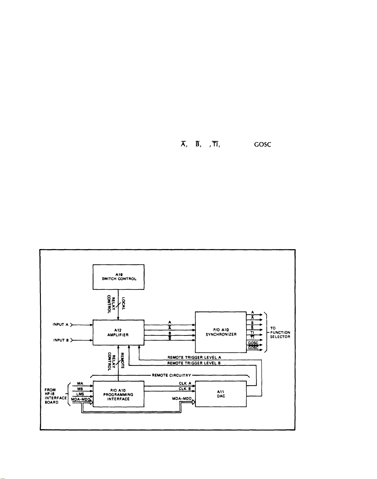
Model 5328A
Theory of Operation
4-107. REMOTE CONTROLLABLE
(PROGRAMMABLE) INPUT BLOCK
DIAGRAM DESCRIPTION
4-108.
I n the local mode, the A19 Switch Control board generates TTL levels that control the
A12 signal conditioning relays. These levels allow front panel control of A and B channel input
signal conditioning. The A19 board accepts inverted A and B channel signals from the A12
board. These signals are routed through pulse stretcher and driver circuits to the A and B chan-
nnel trigger LEDs located on the A19 board. The inverted signals are also translated from ECL to
TTL levels and supplied to the A and B marker outputs.
4-109. Input circuitry for the A and B channels is on the A12 Amplifier board and part of the
A10 Synchronizer board. The A12 board contains the 100 MHz A and B channels with signal
conditioning SLOPE, AC/DC, ATTENUATORS, SEP/COM, amplifiers, and Schmitt triggers.
Signal conditioning circuitry is controlled by relays K1 through K12 synchronizing circuitry for
period and time interval type measurements. The A,
B, ~, TI
,~,
GOSC, and
GOSC
outputs,
~,
from the A10 board, are routed to the A4 Function Selector.
4-110. The programming interface section of A10 board is used to allow remote control of all
input signal conditioning relays. The A11 DAC board contains two identical DACs, A and B
channel, that allow remote control of trigger levels. The outputs of these DACs are supplied to
a relay on the A12 board. In remote, the relay connects these DAC levels to the Schmitt trigger
on the A12 board. There are two modes of accepting remote commands, the non-DAC and DAC
control modes.
4-111. When the 5328A goes into remote, front panel switch control is disabled. At the same
time, the programming interface takes control of the input signal conditioning relays. In the
non-DAC control mode, the interface accepts and decode serial data bytes, stores the infor-
mation in latches, and control signal conditioning via the latched outputs.
4-14
Figure 4-9. Remote Controllable (Programmable) Input Block Diagram
Page 58

Model 5328A
Theory of Operation
4-112. When the interface receives a data byte, for control of trigger levels, it goes into the
DAC control mode. This is a result of the interface receiving a + or - on its input data lines. Once
in the DAC control mode, the programming interface latches disregard the information at their
input. Simultaneously, the information, on the input data lines (MDA-MDD) is accepted by the
A11 DAC board.
4–113. The A11 DAC board shifts the polarity indicator and three following numerical bytes
of information into its shift registers. Following the polarity indicator and the three numerical
data bytes, an asterisk (*) appears on the MDA-MDD lines (see Table 4-7 for proper format).
The asterisk causes the programming interface to revert back to the non-DAC control mode.
In this mode, the All board stops accepting data, and the programming interface latches again
accept the input data.
Table 4-1. 5328A Input Circuit Program Code Set
Programming is accomplished as detailed in Section Ill with the additions below. Codes
shown underlined are start up conditions. These conditions are set by the code “P”, Remote
Programm Initialize, or by the bus commands Device Clear, or Selected Device Clear.
Commands to A channel are preceded by A
Commands to B channel are preceded by B
Trigger levels are programmed using the following format
±X.Y Z*
Where X is volts
Y is 100 s of mV
Z is 10 x of mV
* is used to terminate inputs to the DAC’s
Control
Coupling
Function
AC
DC
Slope
+
Code
2
3
4
5
Atten
Separate/Corn
Separate
Common A
X1oo
X1o
x1
1
6
7
A8
A9
NOTE
Underlined codes are default conditions.
Invert
Normal
A&B Inverted
B8
B9
The check function overrides all other programming commands for A&B channels.
EXAMPLES:
The instruction:
CMD “?U9”, “PF:G5S137A3579-1.25*B37+1.65*R”
Input circuits related programming information
Will program a 5328A with listen address of 9 to:
Function
Time Interval Avg A to B
Multiplier
103
Channel A
DC Coupled
-Slope X1 Atten
Multiple measurement X1 Atten
Continuous Cycle
Manual sample rate control
Common A
Trigger Level -1.25V
Channel B
DC Coupled
Trig Level +1.65V
+Slope
4-15
Page 59

Model 5328A
Theory of Operation
4-114. The A11 DAC board processes the four serial data bytes, and produces one parallel
BCD output. The BCD output provides the information for generating a square wave train by
using a series of rate multipliers. The square wave train has an average duty cycle proportional
to the input code supplied to the rate multipliers. This square wave train switches on a precision current source that feeds a voltage averager to produce a dc output.
4-115. REMOTE CONTROLLABLE (PROGRAMMABLE)
INPUT SCHEMATIC THEORY
4-116. Theory of operation for the programmable input section is given in the following
paragraphs.
4-117. A19 Switch Control Board
4-118. In local mode, -0.7 volts is applied to switches S1-S8. This potential allows the switches
to control their respective functions by supplying an active low available at each switch. In a
closed switch position, the -0.7 volts will forward-bias the associated diode, pull the anode low,
and cause a low to be sent to the amplifier board through J3.
4-119. In remote mode, the -0.7 volts switches to +5 volts, only allowing the output lines, transmitted through J3, to be high. When a switch is open, the pull-up resistor on the line causes it
to go high. When the switch is closed, the associated diode is reverse biased and the line remains high,
4-120. Trigger LEDs, DS1 and DS2, are driven by the inverted A and B outputs of the Schmitt
trigger (A12U4). These signals enter pins 14 and 10 of ECL-to-TTL translator U1. Feedback
capacitors C8 and C9 stretch the 5 nanosecond ECL pulse to approximately a 25 millisecond
TTL output pulse. This 25 millisecond pulse is of long enough duration to be seen, and is used
to drive the trigger LEDs. Since this pulse stretcher is decoupled to the Schmitt trigger, it functions
like a logic probe with adjustable threshold voltage. When Channel A input is higher than the
trigger level setting, the trigger LED is ON. When the input is lower, the LED is OFF, and whenever it passes through the trigger threshold, the LED flashes on or off depending on the polarity
of the input signal.
4-121. The 5 nanosecond inverted A and B outputs are also applied to pins 2 and 6 respectively
of U1. The signals are translated from ECL to TTL levels and connected to the marker outputs.
4-122. A12 Amplifier Board
4-123, Since both A and B channel circuitry are identical only the A channel will be discussed.
4-124. Input signal A enters A12 through J2 and depending on relay K7 is either ac coupled
through capacitor c30 or dc coupled across relay K7. The signal then enters the three position
attenuator (X1, X10, X100) and is passed from the selected attenuation node through either K2,
K3, or K8 to the input of the FET impedance converter stage. Diodes CR5 and CR6, resistors R39,
R37, and R34, and capacitors C23 and C24 form an overvoltage protection network to limit the
signal sent to FET transistor Q3 and successive circuits to ±2.61 volts maximum, The signal at
the node between resistors R30 and R32 follows closely the signal at the gate of Q3A. A potentiometer is used to adjust any initial offset voltage.
4-16
4-125. SEP/COM A relays, K4 and K5, connect the input of the B channel attenuator to either
the A or B channel inputs. The signal then passes through U4, a dual Schmitt trigger, Trigger
U4B compares the signal at pin 9 to a dc reference between ±2.5 volts on pin 10. This dc reference
is selected by K1 and is supplied by either the A11 DAC board or by the A19Switch Control board.
The output of U4 changes state whenever the input crosses the reference voltage on U4(11).
The output is ECL (=-0.8 to -1.6V) and drives both the A trigger LED circuit on the A19 board
Page 60

Model 5328A
Theory of Operation
and the exclusive OR gate U2. Schmitt trigger U4 has approximately 15 mV peak-to-peak
hysteresis at its input. Exclusive OR gate U2 is used to select the desired slope of the input
waveform. When pin 7 of U2 is held to an ECL high level (SLOPE switch in + position), U2 acts
as an inverter. When pin 7 goes low (SLOPE switch in the - position), U2 does not invert the
signal passing through it.
4-126. Input signal conditioning control is accomplished by inverters U1 and U3 and relays
K1-K12. This control is supplied from either the A10Synchronizer board or the A19Switch Control board. When the 5328A is in remote, relay control is received through J1 from the A10 board,
In the local mode, relay control arrives via P2 from the A19 board. Since all of the relay control
lines contain inverters, relay activation is caused by a high at the input.
4-127. A10 Synchronizer Board
4-128. The differential A channel outputs from A12U2 feedthrough connector P2 pins 7 and
8 respectively to U1. Circuit U4 is a one-shot that only triggers on a negative edge, and therefore,
passes only trigger events that occur on the slope selected by A12U2. The output of U4 pin 15
is an ECL pulse of approximately 5-10 nanoseconds width. In the FREQ A check mode, the
oscillator signal from U1(2), (either 10 MHz or 100 MHz as selected by S1) is injected via U5B
to U10(13). The normal A input entering U10(12) is disabled at A12U4 by LCHK being low. The
oscillator signal at U10(13) is passed through U10C and U10D to U11 a dual 4 to 1 multiplexer.
In a noninverting mode, multiplexer U11 always routes the A channel signal to the start synchronizer U6A. In a period function, U11 routes the A channel signal to the stop synchronizer
U6B. For time interval measurements, the B channel signal is supplied to stop synchronizer U6B.
ROM line R6 controls the stop synchronizer input switching. In remote, HINV, from U11(7)
allows the A and B channel outputs of U11 to be inverted. The outputs of U11A feed U12A
which drives the A and A outputs to the A4 Function Selector.
4-129. In Tl, TI AVG, PER, and PER AVG functions, U5, U6, U12, and U13 are used to generate synchronized time interval and gated oscillator pulses for the mainframe. After a reset pulse
arrives on the HDS line, the RS FFs US and U12 and D FFs U6A and U6B are reset. At the same
time, the and GOSC outputs are at an ECL high. When a start event enters U5D pin 12, it sets
the U5A output to U6A pin 7 high. The next clock pulse to U6(6) will cause U6A pin 3 to go low.
This pulls the output low, signaling to the function selector that the time interval has started,
When TI goes low, GOSC (U13B) starts to output oscillator pulses. When a stop event occurs
at U5(10), the output of U12C goes high. This, synchronous to the next clock pulse, sets U16(15)
high. When U16(15) goes high, the TI and GOSC outputs go high stopping the time interval
measurement. The Q output of U6B through U13C, U14B, and U14A resets all FFs and thus
prepares them for the next measurement.
4-130. ROM line RL6(HC), connected to U14(11) by R6, is used in period measurements. This
line is set low in period, and holds the stop FF (U5C and U12C) off until the start synchronizer
U6A clocks a high to its Q output.
4-131. In a PER AVG function where time base scaling takes place, ROM line RL5(T10) is
driven high. This TTL high is converted to an ECL high, by resistors R18 and R21, and applied
through U14D to U12(1)). This causes the stop synchronizer flip-flop (U5C and U12C) to remain
in a reset condition.
4-132. The programming interface has two operational modes, the non-DAC and DAC control
modes. These modes refer to the operation of the interface with respect to incoming data.
When the incoming data is for control of signal conditioning (not trigger level) the interface
will be in the non-DAC mode. The interface will be in the DAC control mode when incoming data
is for DAC (trigger level) control.
4-17
Page 61

Model 5328A
Theory of Operation
4-133. When the 5328A goes into remote, LEXT goes low. The low, on LEXT, causes the output
of A1 Motherboard switch control circuit to go from -0.7 volts to +5 volts. This change, disables
front panel switch control on the A16 and the A19 boards. When LEXT is low, U17(4) connected
to tri-state buffers U2 pin 1 and U9 pines 1 and 15 is also low. This low, returns the outputs of
tri-state buffers, U2 and U9, to their active state. With the outputs of U2 and U9 enabled, the
outputs of addressable latches, U8 and U15, control the A12 signal conditioning relays.
4-134. The interface is reset by a high on the HRPR line. This high is generated by the A15
HP-IB Interface Board when it receives an ASCII “P”.
4-135. When the interface is reset it defaults to the non-DAC control mode. The reset causes
the latched outputs of U8 and U15 to go low. This sets U17 pins 9 and 10 low, giving a low at
U17(8), The low at U17(8) is connected to U7(14), where it causes the interface to be in the nonDAC mode. The low at U17(8) is also connected to clock multiplexer U16(1) where it causes U16
to route clock (LMS) pulses to only U8 or U15.
4-136. Clock multiplexer U16 decodes the MA and MB lines, from the A15 board, to determine
whether the input data byte, on MDA-MDD, is A or B channel information. It then routes the
clock pulse to U8(14) for A channel information, or to U15(14) for B channel information. The
clock pulse, latches the information into the intended latch.
4-137. After reset, the interface defaults to all of the underlined functions in Table 3-5 Pro-
gram Code Set. To change one of the signal conditioning controls it is necessary to program
that function.
4-138. As an example, assume a Channel A function setting of X1 is desired. This means that
an “A7” must be included in the data string sent by the system controller to the 5328A. When the
“A” is decoded by the A15 HP-IB interface, it causes the MA line to be high and the MB line to
be low. The MA and MB lines are decoded by U6 and it routes the following clock pulses to U8.
4-139. When the “7” is sent, 1110 appears at the input of ROM U7 on MDA-MDD respectively.
As shown in Table 5-28, the 1110 at the input causes an output of 000011 on U7 pins 1-6.
4-140. The clock pulse arrives at U8(14) and latches the high on U8(13) to U8(5). The high on
U8(5) is buffered by U9 and appears at pin 13 of its output. The high at U9(13) is inverted on the
same function as Channel A.
4-141. All non-DAC information is latched in the same manner. B channel information is
latched into the outputs of U15. it has the same code into U7, and thus the same code out of U7,
for the same function as Channel A.
4-142. Refer to Table 3-5 Program Code Set for the proper format to program a trigger level.
The proper format is ±X.YZ*, and follows an A and B which indicates to which channel it
applies.
4-143. For the following discussion, assume a trigger level is programmed, following the
proper format, and preceeded by an “A”,
A15 board receives an ASCII “P” from the system controller. When the A15 board receives the
“A”, the MA line is set high and the MB line is set low. U16 decodes the MA and MB lines, in the
non-DAC mode, and clocks the A channel latch U8.
The interface resets to the non-DAC mode when the
4-18
4-144. When a + or - appears on the MDA-MDD lines, a high is latched into U8(12), Latching
occurs on the positive clock pulse transition from U16. The high at U8(12), will cause U17(8) to
go high. U17(8) is connected to U7(14), where the high changes the input address to ROM U7,
and locks the interface into the DAC control mode. The high at U17(8) is also connected to
U16(1). A high at U16(1) causes U16 to supply clock pulses to either the A or B channel DAC.
Page 62

Model 5328A
Theory of Operation
Since the condition of the MA and MB lines remains the same, the Channel A DAC receives
the clock pulses. On the negative transition of the clock pulse, the + or - is shifted into the A
channel DAC shift registers A10U7 and U11.
4-145. Following the format, the next data byte on MDA-MDD will be a number. The MDAMDD lines supplied to U7 are also connected to the A11 DAC board shift registers. Since the
interface is in the DAC mode, neither U8 or U15 are clocked and thus disregard data on MDAMDD. The number is clocked into the A channel DAC shift registers. The condition of the MA
and MB lines, determines which DAC is clocked and accepts the number. Following the first
number, a decimal appears at the input to ROM U7. When U7 decodes the decimal, it sends
U7(5) high. This high, applied to U2(15), causes U2 to block the clock pulse associated with the
decimal data byte.
In this manner, the DAC disregards the decimal.
4-146. Following the format, two more numbers are input, serially, and each clocked into the
A channel DAC shift registers. The final character in the string, an asterisk (*), appears on the
input data lines to U7. When U7 decodes the asterisk, U7(5) goes high, again blocking the
positive clock pulse transition to the A channel DAC. This causes the A channel DAC to disregard the *. Simultaneously U7(6) goes low, allowing the negative transition of the clock pulse
to latch the low at U8(13) into U8(12). The low at U8(12) causes U17(8) to go low, returning the
interface to the non-DAC control mode.
4-147. A11 DAC Board
4-148. Since the DAC board contains two identical DACs only the Channel A DAC will be
discussed. For the following description assume the Channel A DAC is programmed for a
+2.22V trigger level. Refer to Program Code Set, Table 3-5, for an explanation of the format.
4-149. The first data byte, a +, appears on the input data lines MDA-MDD. This data byte is
supplied to the inputs of shift registers U7 and U11. An LMS clock pulse routed through A10U6,
applied to U7 pin 1, shifts the + into U7 and U11. The next three data bytes, all two’s, are shifted
into U7 and U11 in the same manner.
4-150. With the + and the three numerals shifted into U7 and U11, the shift registers provide
a parallel BCD output. This parallel output is static until the A channel DAC is reprogrammed.
The parallel output is supplied to the input of rate multiplier chain U8, U9, and U10.
4-151. Circuit USC and related components are configured as an oscillator. The oscillator
output is coupled through Q7 to the clock input of rate multipliers U8, U9, and U10. The clock
signal is also supplied through inverter U5D to D-FF U2A, which is used as a synchronizer and
wave shaper.
4-152. With 1000 pulses entering pin 9 of each rate multiplier, the output at U10(6) will be
222 pulses, These pulses are supplied through level shifter and inverter U5B to U2(12), The in-
put pulese are synchronized and shaped by U2A, The Q and Q outputs, from U2A, supply level
shifter networks composed of resistors R31, R34, and R36, R38, and R39. The pulse outputs
from the level shifter networks arrive at the cathode of CR6 and the anode of CR8.
4-153. The + shifted into U11, causes U6 pins 2 and 6 to go high, The highs, on pins 2 and 6,
cause pins 1 and 7 to go low. The low at U6(1), causes CR11 to be forward biased. Forward bias-
ing CR11 causes U6A to sink all of the current from the positive current source, This disables
the positive current source U3A and Q3. With U6(7) low, CR12 is reverse biased enabling the
negative current source U3B and Q4.
4-154. The signal at the anode of CR8 is the inverted output from the rate multipliers. When
the anode of CR8 is low, CR8 is reverse biased, and current flows through CR10 into U4(2), When
the anode of CR8 is high, CR8 is forward biased and current flows from Q4 through CR8
4-19
Page 63

Model 5328A
Theory of Operation
4-155. Averager U4 converts the current pulses supplied via CR10 into a dc output voltage.
The averager generates the output voltage proportional to the duty cycle of the input current
pulses.
4-156. A8 Channel C Input
4-157, The A8 board contains circuitry to amplify and detect input signals up to 500 MHz, a
divide-by-10 counting chain, a high-speed gate, and circuitry to drive the least-significantdigit in the display.
4-158, The input signal enters J1 and continues through a fuse (F1) into a limiter circuit composed of diodes CR2-5 and a 50-ohm termination. Diodes CR2-5 have 70V reverse breakdown
voltage and limit the signals below that value to approximately ±600 mV to protect amplifier
U1. Fuse (F1) is rated at 125 mA and blows when the input voltage reaches about =7 volts. The
signal passes through amplifier U1 (with a single ended gain of =4) and drives U2 (a combination
amplifier/Schmitt trigger) differentially. The Schmitt trigger output (U2 pin 13) is a logic level
from 0 volts to approximately -600 mV. The now digital (square wave) signal passes through
U3 where it branches to drive a binary (U4) and a detector. The detector circuit senses the
presence of an input signal and sends a TTL “C ARM” command to the A4 Function Selector,
as described in the following paragraph.
4-159. During normal operation (in the frequency C function) U4 is originally disabled by a
High logic level at U4 pin 14 (0 volts). When the counter is ready to make a measurement and
it senses that an input signal is present via the “C ARM” line, the main gate opens. Pin 14 on
U4 then goes “low” (to -600 mV) and the input signal passes through U4
lated to ECL levels. A 50-40% duty cycle (for sine wave inputs) signal is sent to the A4 Function
Selector on “C” and
14 goes high and U4 and U5 stop in their present states. Circuit U6 translates the information in
U4–U5 to TTL level and it is shifted into a quad latch (U7) where it is stored for strobing into
the display.
(+5)
where it is trans-
“~”
bus lines, after the time base counts out, the main gate closes, U4 pin
4-160. Circuit U10, Q1, Q2, and various resistors constitute a current source to properly bias
U1 and U2. The circuit draws approximately 16 mA out of pin 3 on each IC and adjusts the current out of pin 6 between 28 and 56 mA until the voltage on pin 3 is approximately +600 to
+900 mV on each IC.
4-161. Resistors R1, R2, R4, and R82 and U9A comprise the offset voltage adjustment circuit.
This circuit also compensates for changes in input bias current into U1 to minimize drift in
offset voltage.
4-162. HP INTERFACE BUS THEORY
4-163. The HP Interface Bus transfers data and commands between the components of an
instrumentation system on 16 signal lines. The interface functions for each system component
are performed within the component so only passive cabling is needed to connect the system.
The cables connect all instruments, controllers, and other components of the system in parallel
to the signal lines.
4-164. Eight of the lines (DIO1—DIO8) are reserved for the transfer of data and other messages
in a byte-serial, bit-parallel manner. Data and message transfer is asynchronous, coordinated
by the three handshake lines (DAV, NRFD, NDAC). The other five lines are for control of bus
activity,
4-165. Devices connected to the bus may be talkers, listeners, or controllers. The controller
dictates the role of each of the other devices by setting the ATN (attention) line low and sending
4-20
Page 64

Model 5328A
Theory of Operation
talk or listen addresses on the data lines (DIO1—DIO8). Addresses are set into each device at
the time of system configuration either by switches built into the device or by jumpers on a
PC board. While the ATN line is low, all devices must listen to the data lines. When the ATN
line is high, only devices that have been addressed will actively send or receive data. All others
ignore the data lines.
4-166. Several listeners can be active simultaneously but only one talker can be active at a
time. Whenever a talk address is put on the data lines (while ATN is low), all other talkers will
be automatically unaddressed.
4-167. Information is transmitted on the data lines under sequential control of the three handshake lines. No step in the sequence can be initiated until the previous step is completed.
Information transfer can proceed as fast as devices can respond, but no faster than allowed by
the slowest device presently addressed as active. This permits several devices to receive the
same message byte concurrently.
4-168. The ATN line is one of the five control lines. When ATN is low, addresses and universal
commands are transmitted on seven of the data lines using the ASCII (American Standard
Code for Information Interchange) code. When ATN is high, any code of 8 bits or less understood by both talker and listener(s) may be used.
4-169. The other control lines are IFC, REN, SRQ, EOI. IFC (interface clear) places the inter-
face system in a known quiescent state. REN (remote enable) is used with other coded mes-
sages to select either local or remote control of each device.
4-170. Any active device can set the SRQ (service request) line low. This indicates to the controller that some device on the bus wants attention, say a counter that has just completed a
time-interval measurement and wants to transmit the reading to a printer.
4-171. EOI (end or identify) is used by a device to indicate the end of a multiple-byte transfer
sequence. When a controller sets both the ATN and EOI lines low, each device capable of a
parallel poll indicates its current status on the DIO line assigned to it.
4-172. For a more detailed description of bus operation, refer to the manual entitled “Con-
densed Description of the Hewlett-Packard Interface Bus”, HP Part No. 59401-90030.
4-173. HP-IB A15 INTERFACE OPERATION
4-174. The 5328A HP-IB Interface is used to remotely program the 5328A and deliver the measurement results to the bus. Thus, the board operates both as a listener and as a talker.
4175. As a listener, the interface is capable of programming most of the controls in the
mainframe and all programmable modules that may be installed. The HP-IB board contains
storage circuits to control the mainframe remotely, and is set up to program the storage circuits
in any programmable module.
4-176. As a talker, the interface is capable of outputting the measurement data in exponential
format with a mantissa of nine digits (leading zeros are output as spaces) and an exponent of
one digit. Overflow and signal information is also contained along with a carriage return (CR),
linefeed (LF) termination ot make it compatible with the standard HP-IB serial data format.
4-177. In addition to being a talker and listener, the HP-IB Interface follows a set of HP-1 B
commands. This includes complete service request capability, The ASCII codes used for addressing and for data are shown in Table 3-7. Address switch information is shown in Table 3-4.
The program code set is shown in Table 3-5.
4-21
Page 65

Model 5328A
Theory of Operation
4-178. Overall Operation
4-179. The heart of the HP-IB Interface is a 256 state algorithmic state machine (ASM) con-
trolled by a 256x16 ROM (U22) as shown in the block diagram. This state machine has two dif-
ferent format states determined by the format (F) bit from U22. One state (F=0) is an output
mode state where the machine will proceed sequentially to the next state (address) after storing
or outputting information. The other state (F=1) is a mode where the machine can either proceed to the next line or perform a conditional jump to a different line in the program. The decision as to which state is chosen is made on the basis of where the qualifier bit from U11A is
low or high. Preset counters U14 and U23 provide presetting to a jump state when F=1 and the
qualifier is low. These counters increment their count in all other cases. Altogether, there are
52 different bits that may be selected as the qualifier for a particular state.
4-180. Qualifier negate circuit U30C can invert the qualifier bit for any given state so that the
machine can branch on the qualifier being low or being high. U7 is added for psuedo subroutine capability. In the output mode, the ASM goes through the same group of states once
for every character being outputted on the bus. U7 is incremented every time so that the ASM
can tell which character it is to output.
4-181. Bus Command Mode
4-182. In this mode (ATN low), the ASM accepts parallel bytes of information and decodes
them into bus commands. This usually requires setting or clearing bits of storage in U19 or U26.
4–183. Listen Mode
8-184. In the listen mode, the listen qualifier of U26 must be low and ATN high. The interface
will then accept 8-bit parallel bytes continuously. When receiving the ASCII characters P, Q,
U, R, or T the counter will act upon the byte immediately (refer to programming in Section Ill).
When receiving the letters F, G, A, B, C, D, or S the interface will then route any ASCII number
or numbers following these letters into particular storage registers. These registers are U28,
U33, and U34 along with any that are contained in any of the optional modules installed in the
mainframe.
4-185. Talk Mode
4-186. The HP-IB Interface will go into the talk mode if the talk qualifier of U26 is low or the
talk always switch is set to talk always and ATN high for both cases. There will be no output in
normal operation unless a completed measurement is present and has not been outputted. The
information to be put on the bus is latched into latches U15 and U24. These drive the high current buffers U5
U10, and U16, Counter U7 is used as a pointer for the ASM to recognize which
)
character in the serial output string the interface is to output.
4-187. A15 Circuit Operation
4-188. The following paragraphs describe the circuit operation of the HP-IB Interface.
4-189. STATE COUNTERS. The state of the ASM ROM (current state and next state) is deter-
mined by State Counters U14 and U23. These counters from an 8-bit presettable binary counter,
When pin 1 of U25 is low, the counters will always increment. When pin 1 of U25 is high, the
counters will preset (jump to another state in the program) if the output of U30C is high. The
preset address is supplied to the State Counters input from the ROM. The program is shown
in the operational flowchart, Figures 5-4, 5-5, and 5-6. The output of U30C is determined by
the “not” bit from the ROM (through U21E) and the output of the Qualifier FF U11A. The preprogrammed state of the “not” bit determines whether a high or low output of the qualifier
FF will result in a jump in the program. (This is shown in the ASM Operational Flowchart, by
4-22
Page 66

Model 5328A
Theory of Operation
the use of the letter “N” in a decision diamond symbol. ) The preset (jump) is synchronous and
only occurs when pin 9 of U14 and U23 is low and when there is a rising edge at pin 2 of U14
and U23. FF U31A synchronizes the reset of the State Counters to occur at the proper time.
4-190. ASM OSCILLATOR. As shown in the ASM Oscillator Timing Diagram, Figure 4-70,
the ASM oscillator circuit provides three separate phases of clock outputs. Schmitt trigger
U18A is the fundamental oscillator element which uses hysteresis to develop oscillation, The
output of U18A (through U13) strobes storage latches U11A and B, U15, U19, U24, U26, U28,
U33, U31B, and U34. The output of U18A is also sent through a delay circuit consisting of resistor R14 and capacitor C4 into U18B to provide another phase of the clock output that deter-
mines the next state of the ASM. In addition, the output of U18A is sent through U30A to provide a third clock phase which is applied to U31A. The output of U31A resets the 8-bit State
Counter synchronously at power up or when the IFC signal occurs. (Synchronous reset prevents
loading the storage latches with erroneous data.) The IFC signal also resets U26 (ASM storage).
The power up reset circuit U18C and U18D clears all storage elements.
4-191. BUS INTERFACE. The bus interface circuit consists of bus line termination resistors,
data output drivers and data input buffers. Resistors R29 and R30 form the line termination networks, U4 is used to buffer the bus line inputs and U5, U10, and U16 are high current drivers
that drive the bus lines output. The ATN signal is sent through U9A and U29D to ensure that
the gates connected to bus lines DIO1—DIO7 and DAV do not output when ATN goes true. The
DAO signal from U24(9) arms the DAC signal through U17B to ensure that DAC goes false
within a few gate delays after ATN goes true. (1 n some cases, the DAC response from the ROM
may be too slow.) After ATN is true, DAO is set to a “0” to allow normal operation of the DAC
line.
4-192. END OF MEASUREMENT. When a measurement has been completed, FF U11B is set.
This FF is clocked by the closing edge of the LMG signal. Diode CR2 and transistor Q3 keep U11B
from going to the “l” state when LRES is low or HRD is high, (During these times the counter
is being reset and noise appears on the LMG line which could trigger UIIB.)
4-193. QUALIFIER MULTIPLEXER. Five 8-to-1 multiplexer are connected to allow 36 lines
to be multiplexed into 1 line. ASM ROM U22 controls multiplexer U3, U6, U8, and U32 to
select individual line qualifiers and U12 to select one of these multiplexer. In addition, U12
checks the output of auxiliary State Counter U7, a 4-bit binary counter that allows the same
sequence of states to be repeated up to 16 times. In the output algorithm, each state represents
an output character. Qualifier FF U11A eliminates erroneous results by ensuring that the State
Counters U14 and U23 are not clocked when a qualifier is changing states. This would cause a
partial preset and partial increment of the State Counters,
4-194. ADDRESSING. Address Comparator U2 monitors the Data Input/Output (DIO) lines
2 through 5 and the address switch (S1) settings. When a comparison occurs between the state
of these DIO lines and the address switch settings, U2 sends qualifier ADDR to multiplexer U8.
The TALK ALWAYS section of the address switch provides a means of setting U6 so that inter-
face is always addressed to talk.
4-195. DATA OUTPUT. The Data Output circuit outputs characters on the bus data lines.
Storage circuit U24 transfers outputs from the ROM to DIO lines 5 through 7. U15 selects data
from either the ROM or the 5328A data bus and transfers it to DIO1—DIO4. The state of the “not”
bit from ROM U22(13) through U21E determines the selection made by U15. A displayed digit
is selected from the 5328A, any other characters (decimal point,
linefeed, etc.) are selected from the ROM.
“E”, carriage return, exponent,
4-196. ASM STORAGE. The internal memory for the ASM operation is in ASM Storage circuits
U19, U26, and U31B. There are 17 information bits that can be set or cleared by these circuits.
This section also includes one-shot U1 which outputs a 2 ms pulse (LRST) to ensure reliable
4-23
Page 67

Model 5328A
Theory of Operation
operation of the state control circuit U4 on the motherboard. Diode CR3 ensures that LINH is
low to inhibit the counter during the time that LRST is low.
4-197. STROBE ENABLE DECODER. Decoder U13 is a 4- to lo-line decoder used to strobe the
various storage latches. Pins 1, 14, and 15 are used to select the device to be strobed and pin 2
is an enable which determines the width of the strobe pulse. The output of U25C disables U13
when the ASM is in the decision state mode. In the decision state mode, the format bit U22(17)
goes high which disables U13.
4-198. REMOTE PROGRAM STORAGE. Storage circuits U28, U33, and U34 are used to program
instrument functions. U28 stores Time Base codes in 3-bit bytes and U34 stores Function codes
in 4-bit bytes. U33 stores 8 bits of information, one-bit at a time. The Sample Rate, Arming,
Storage Off, and Decade Reset can be programmed by U33. In addition, U33(4,5, and 6) control
the manner in which measurements are made and output to the bus. The inputs to the remote
program storage circuits are the Module Data A, B, C, and D lines from DIO lines, 1,2,3, and 4,
respectively.
4-24
Figure 4-10. ASM Oscillator Timing Diagram
Page 68
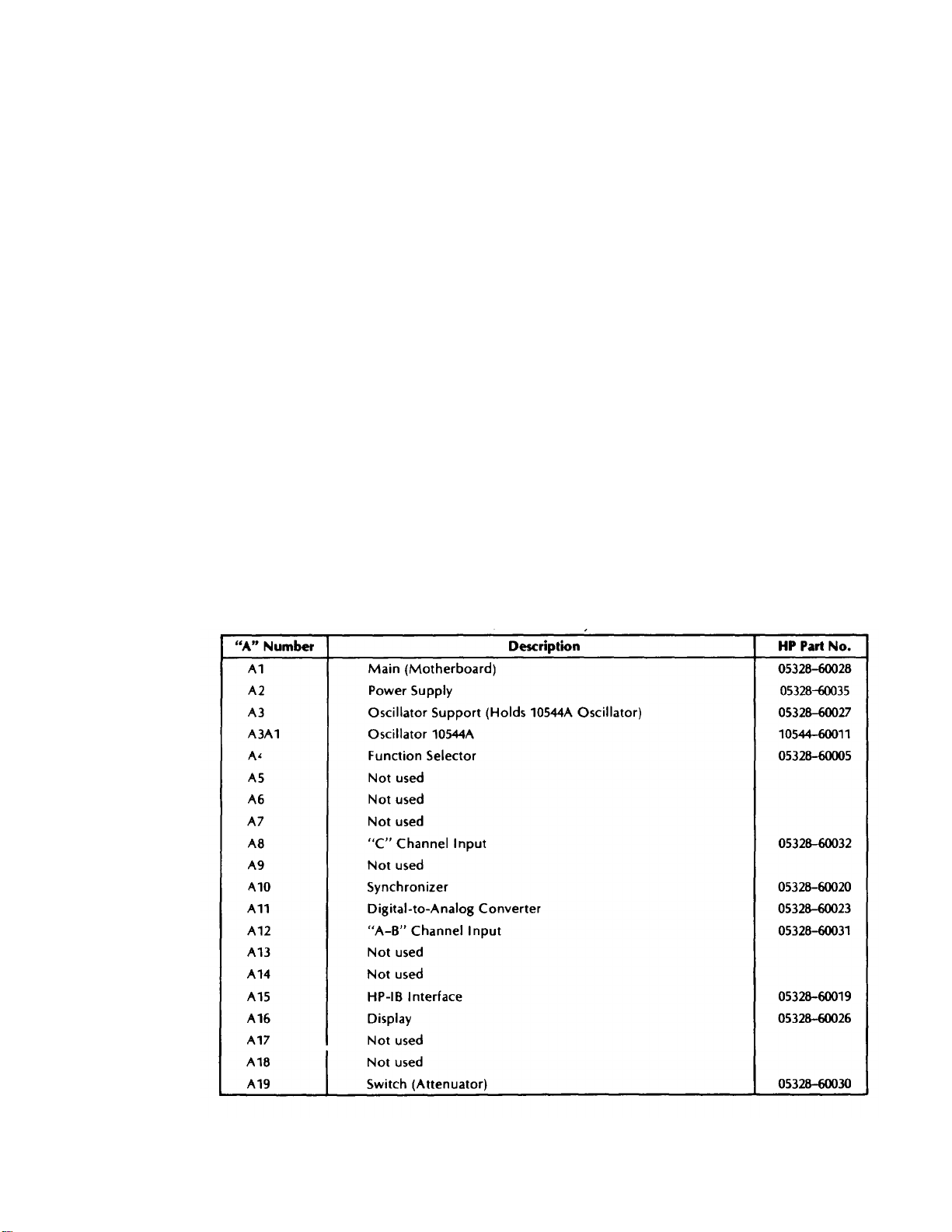
Model 5328A
Maintenance
SECTION V
MAINTENANCE
5-1. INTRODUCTION
5–2. This section gives maintenance and service information. Included is a table of assemblies,
recommended test equipment, a performance test, (which may be used to verify proper counter
operations) and adjustments.
5-3.
5-4.
used
5-5.
5-6.
Table 5-2. Test equipment having equivalent characteristics may be substituted for the equip-
ment listed. Required test equipment is listed in Appendix D, Maintenance
Allocation.
5-7. ASSEMBLY CONNECTION IDENTIFICATION
5-8. Throughout the manual, connections to printed-circuit assemblies are referred to in abbreviated form. For example, connection to A4 pin 10 is A4(10).
ASSEMBLY DESIGNATIONS
Table 5-1 lists the designations, name, and Hewlett-Packard part number of assemblies
in this instrument.
TEST EQUIPMENT
Test equipment recommended for maintaining and checking performance is listed in
Table 5-1. 5328A Assembly Identification
5-1
Page 69
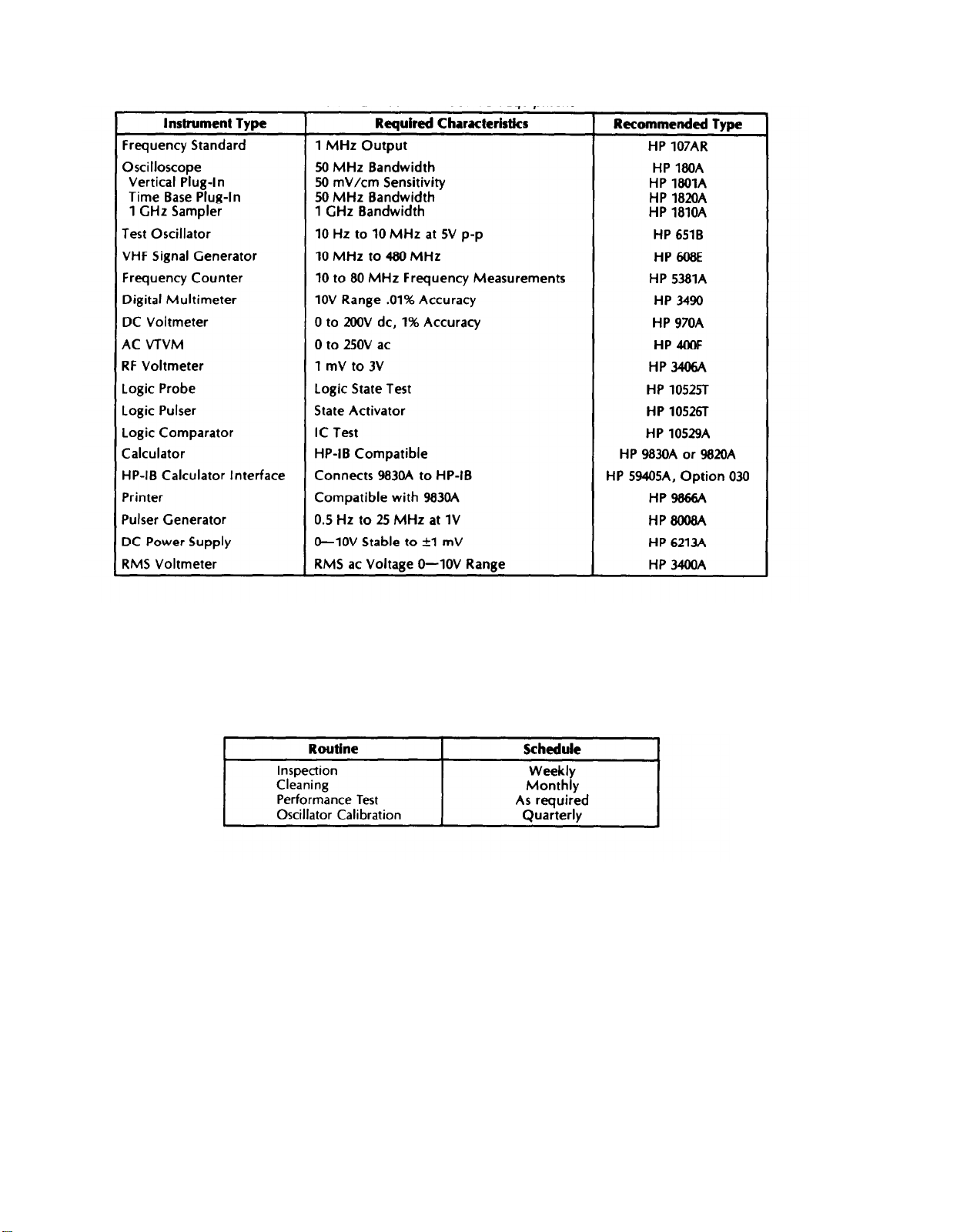
Model 5328A
Maintenance
Table 5-2. Recommended Test Equipment
5-9. PREVENTIVE MAINTENANCE
5-10. Preventive maintenance consists of periodic inspection, cleaning, performance checks,
and oscillator calibration. Table 5-3 lists the recommended schedule of preventive maintenance
routines.
Table 5-3. Preventive Maintenance
5-2
Page 70

Model 5328A
Maintenance
5-11. Inspection
5-12. The 5328A should be inspected for indications of mechanical and electrical defects. Electronic components that show signs of overheating, leakage, frayed insulation, and other signs
of deterioration should be checked and a thorough investigation of the associated circuitry
should be made to verify proper operation. Mechanical parts should be inspected for excessive
wear, looseness, misalignment, corrosion, and other signs of deterioration.
5-13. Cleaning
5-14. The instrument should be kept free of dust, moisture, grease, and foreign matter to
ensure trouble-free operation. A dry clean cloth, a soft bristled brush, or a cloth saturated with
cleaning compound may be used.
WARNING
100/120/220/240 VAC SUPPLY WIRES ARE EXPOSED WHEN
EITHER TOP OR BOTTOM COVER IS REMOVED. USE EXTREME
CAUTION DURING TROUBLESHOOTING, ADJUSTMENT, OR
REPAIR. AVOID DAMAGE TO INSTRUMENT BY REMOVING
POWER BEFORE REMOVING OR REPLACING COVERS, ASSEMBLIES, OR COMPONENTS.
5-15. Performance Test
5-16. GENERAL. The performance test (Table 5-4) and test card sheets that follow the test can
be used to verify and record proper operation of all circuits of the counter and may also be used:
As part of an incoming inspection check of instrument specifications.
a.
b. Periodically, for instruments used in systems where maximum reliability is important.
c.
As part of a procedure to locate defective circuits.
d. After any repairs or adjustments and before returning instrument to regular service.
As a permanent record of instrument maintenance performed, because the test record
e.
pages may be removed.
5-17. REPAIR
5-18. Printed Circuit Component Replacement
5-19. Component lead holes in the circuit boards have plated-through walls to ensure good
electrical contact between conductors on opposite sides of the board. To prevent damage to the
plating and the replacement component, apply heat sparingly, and work carefully.
5-20. Replacing Integrated Circuits
5-21. Following are two recommended methods of replacing integrated circuits:
SOLDER GOBBLER. This is the best method. Solder is removed from board by a solder-
a.
ing iron with a hollow tip connected to a vacuum source,
b. CLIP-OUT. This method should be used as a last resort only. Clip the leads as close to
the base as possible. With a soldering iron and long nose pliers, carefully remove the
wires from each hole. Then clean the holes.
5-3
Page 71
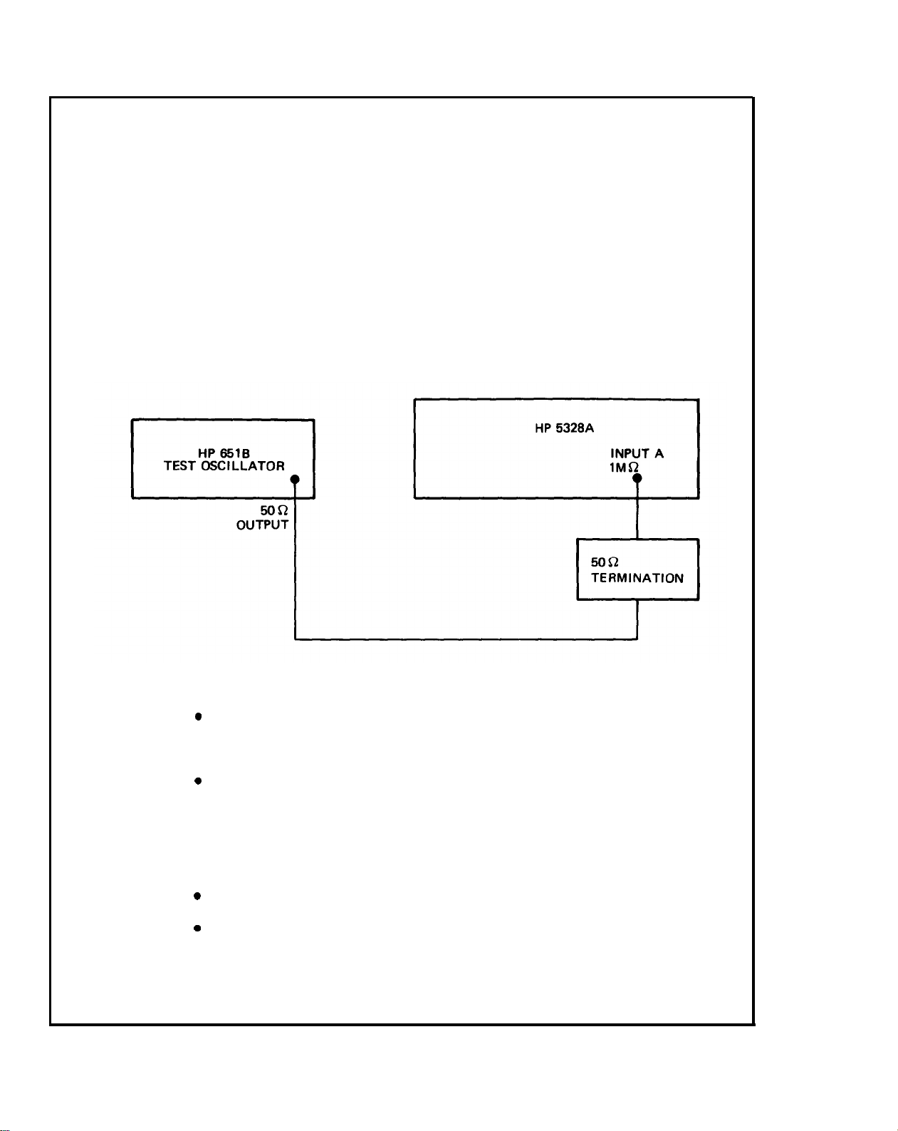
Model 5328A
Maintenance
1. SENSITIVITY - Channel A
Table 5-4. Performance Test
Specification:
15 mV rms, 0-35 MHz (dc coupled)
20 Hz-35 MHz (ac coupled)
50 mV rms, 35 MHz-100 MHz
Description: A signal generator with calibrated output is set to the specified 5328 signal
sensitivity level and varied over the specified frequency range. The counter must display the
correct frequency.
10 Hz to 10 MHz
a.
Setup:
5-4
(1) DC coupled 10 Hz to 10 MHz
l
Set the 5328A to FREQ A, 1 Hz RESOLUTION, SAMPLE RATE fully ccw, Level A
to PRESET, DC COUPLING, ATTEN X1, SEP. Rear panel ARM switch should
be set to OFF.
.
Set the 651B for 15 mV rms. Vary the 651B’s frequency from 10 Hz to 10 MHz
and verify that the 5328A displays the proper frequency. Adjust the 5328 LEVEL
A control as necessary to achieve a stable display. Mark results on performance test record at the end of these procedures.
(2) AC coupled 20 Hz to 10MHz
l
Set the 5328 to AC coupling.
l
Set the 651B for 15 mV rms. Vary the 561B’s frequency from 20 Hz to 10 MHz
and verify that the counter displays the proper frequency. Adjust the 5328
LEVEL A control as necessary to achieve a stable display. Mark results on per-
formance test record at the end of these procedures.
Page 72

Table 5-4. Performance Test (Continued)
10 MHz to 100 MHz
b.
Setup:
(1) DC coupled 10 MHz to 100 MHz
.
Set the 5328A to DC COUPLING.
Model 5328A
Maintenance
.
Set the “8601A for an output level of 15 mV rms as measured on the 3436A
RF voltmeter. Vary the 6601A’s frequency from 10 MHz to 35 MHz and verify
that the counter displays correct frequency readings. Increase the 8601A
output level to 50 mV rms and vary the frequency from 35 MHz to 100 MHz.
Verify that the counter displays correct frequency readings. Adjust 5328A
LEVEL A control as necessary to obtain stable display. Mark results on
performance test record.
(2) AC coupled 10 MHz to 100 MHz
.
Set the 5328A to AC coupling.
l
Set the 8601A for an output level of 15 mV rms and repeat part 2 of step (1.)
above.
2.
SENSITIVITY - Channel B
Specification:
15 mV rms,0-35MHz (dc coupled)
20 Hz-35 MHz (ac coupled)
50 mV rms, 35 MHz-100MHz
Description: A generator with calibrated output drives the B channel of the 5328A under
test. The frequency of the B channel MARKER OUTPUT is measured by a second frequency
counter. The generator is set to the specified 5328A signal sensitivity level and varied over
the specified frequency range. The second counter must display the correct frequency.
Adjustments of the 5328A LEVEL B control may be necessary to achieve a stable count.
5-5
Page 73

Model 5328A
Maintenance
a.
10 Hz to 10 MHz
Setup:
Table 5-4. Performance Test (Continued)
(1) DC coupled 10 Hz to 10 MHz
l
Set counter No. 1 (HP 5328A) to
DC coupling (B channel).
l
Set the 651B to 15 mV rms. Vary the 6516’s frequency from 10 Hz to 10 MHz
and verify that the 5328A Channel B MARKER OUTPUT is the correct frequency
as read by counter No. 2. Adjust the 5328A LEVEL B control as necessary to
achieve a stable display. Mark
(2) AC coupled 20 Hz to 10 MHz
l
Set Counter No. 1 (HP 5328A)
l
With the 651B set to 15 mV rms, vary the frequency from 20 Hz to 10 MHz
and verify that the 5328A Channel B MARKER OUTPUT is the correct frequency
as read by counter No. 2. Adjust the 5328A LEVEL B control as necessary to
achieve a stable display. Mark results on performance test record.
b. 10 MHz to 100 MHz
Setup:
SEP, LEVEL B to PRESET, ATTEN X1 (B channel),
results on performance test record.
to AC coupling (B channel).
5-6
Page 74
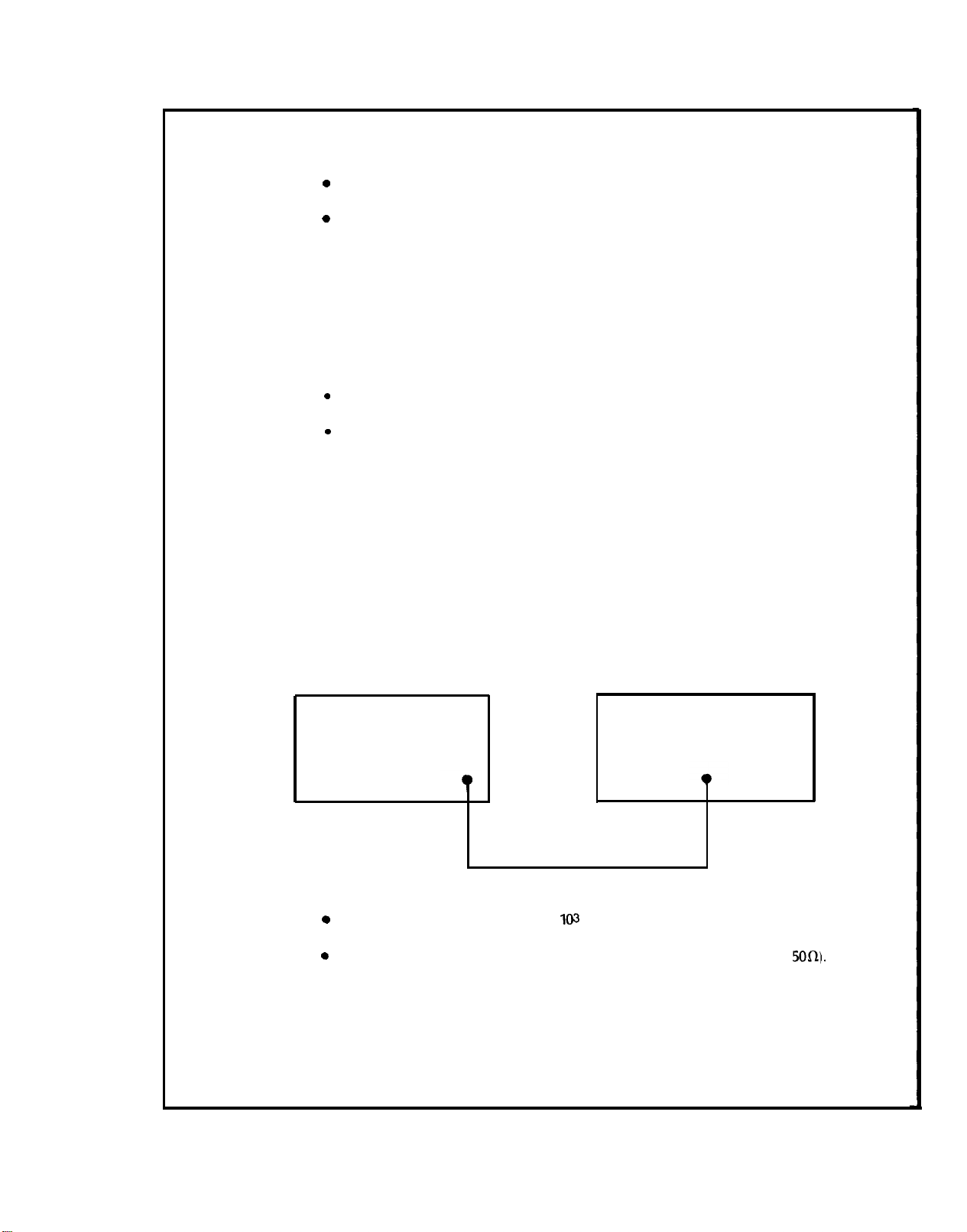
(1) DC coupled 10 MHz to 100 MHz
.
Set Counter No. 1 (HP 5328A] to DC coupling (B channel).
l
Set the 8601A for an output level of 15 mV rms as measured on the 3406A
RF voltmeter. Vary the 8601A’s frequency from 10 MHz to 35 MHz and verify
that the 5328A Channel B MARKER OUTPUT is the correct frequency as read
by counter No. 2. Increase the 8601A output level to 50 mV rms and vary the
frequency from 35 MHz to 100 MHz. Counter No. 2 must continue displaying
the correct input frequency. Adjust the 5328A LEVEL B control as necessary
to achieve a stable display. Mark results on performance test record.
(2) AC coupled 10 MHz to 100 MHz
l
Set Counter No. 1 (HP 5328A) to DC coupling (B channel).
l
Set the 8601A for an output level of 15 mV and repeat part 2 of step (1) above.
3. SENSITIVITY-Channel C
Model 5328A
Maintenance
Table 5-4. Performance Test (Continued)
Specification:
15 mV rms, 30 MHz-500MHz
Description: A signal generator covering the frequency range from 30 MHz to 500 MHz
is set to the specified channel C 5328A signal sensitivity level and varied over the specified
frequency range. The counter must display the correct frequency.
Setup:
HP 8840A
SIGNAL GENERATOR
l
Set the 5328A to FREQ C, 1 kHz,
103
Resolution, SAMPLE RATE midrange.
HP 5328A
CHANNEL C
.
Set the signal generator for an output of 15 mV rms (-24 dBm for
the frequency from 30 MHz to 500 MHz and verify that the counter displays
the proper frequency.
50fl).
Vary
5-7
Page 75

Model 5328A
Maintenance
4. PERIOD AND PERIOD AVERAGE
Specification:
PER A - counter will measure periods of signals to 10 MHz with resolutions from 10 ns to
0.1s in decade steps.
PER AVG A - counter will measure periods of signals to 10 MHz with resolutions from
100 ns to 0.01 ps in decade steps. The number of periods over which the period average
measurement is made can be selected by the FREQ RESOLUTION, N switch.
Description: The 1 MHz time base output from the rear panel of the 5328A drives the A
channel input of the counter.
Table 5-4. Performance Test (Continued)
l
Set 5328A Function switch to PER A; Freq Resolution, N switch to 1 MHz, 1; Level A to
PRESET; AC coupling; X10 ATTEN; SEP. Verify that the counter displays 1.0µsec. Mark
results on performance test record.
l
Set the 5328A Function switch to PER AVG A and the Freq Resolution, N switch to 1 Hz,
I(N.
Verify that the counter displays approximately 999,9XXXX nsec with 0.1 psec reso-
lution. Mark results on performance test record.
5. RATIO B/A, or C/A
Specification:
RATIO B/A, RATIO C/A-Counter will measure the ratio of the frequency at B (0 to
100 MHz) or C (30 to 500 MHz) to the frequency at A (0 to 10 MHz) for N counts of A.
Description: The 1 MHz time base output from the rear panel of the 5328A drives the
A, B or C input channels of the counter.
5-8
Page 76

Setup:
Model 5328A
Maintenance
Table 5-4. Performance Test (Continued)
Set the 5328A Function switch to RATlO B/A: Freq Resolution. N switch to 1 kHz, I@:
Level A and B to PRESET; AC coupling on both channels; X10 ATTEN on both channels;
COM A. Verify that the counter displays 1.000. Mark results on performance test
record.
Set the 5328A Function switch to RATlO C/A; SEP. Disconnect the channel B input and
reconnect it to channel C. Verify that the counter displays 1.000.
6.
TIME INTERVAL AND TIME INTERVAL AVERAGE
Specification:
T.I. A-B - counter measures time intervals (100 ns to
channel A input and a stop signal at the channel B input.
T.I. AVG A-B - counter measures time intervals (0.1 ns to 10 see) between a start signal
at the channel A input and a stop signal at the channel B input. The number of time
intervals over which the time interval average measurement is made can be selected by
the FREQ RESOLUTION, N switch.
Description: A 1 MHz signal drives the A and B channel inputs of the 5328A counter.
108
see) between a start signal at the
5-9
Page 77

Model 5328A
Maintenance
7. GATE/MARKER OUT AND SAMPLE RATE
Table 5-4. Performance Test (Continued)
l
Set the 651B to 1.0 MHz and 500 mV rms.
.
Set the 5328A Function switch to T.I. A-B; Freq Resolution, N switch to 1 MHz, 1; Level A
and B to PRESET; AC coupling on both channels, X1 ATTEN on both channels, COM A.
l
Set the Channel A SLOPE to (+) and the Channel B SLOPE to (–). Verify that the
counter displays 0.5 µs ±0.25 µs. Mark results on performance test record.
l
Set 5328A Function switch to T.I. AVG A+B and Freq Resolution, N switch to 1 Hz,
Verify that the counter displays 500.XXXX ns. Mark results on performance test record.
l
Change Channel A SLOPE to (-) and Channel B SLOPE to (+). Verify that the counter
displays 500.XXXX ns. Mark results on performance test record.
Setup:
I(F.
5-10
l
Set the 5328A to CHECK, 1 kHz, l@ Resolution.
l
Observe the GATE/MARKER OUT signal from the counter. Vary the SAMPLE RATE
control to full ccw. The GATE/MARKER OUT signal must be greater than 2.4 Vdc and
the sample delay (time during which GATE/MARKER OUT is Low) must be less than
2 msec. Mark results on performance test record.
Page 78
Table 5-4. Performance Test (Continued)
8. REMOTE PROGRAMMING TEST
Setup:
Model 5328A
Maintenance
5-11
Page 79
Model 5328A
Maintenance
Table 5-4. Performance Test (Continued)
.
Set the pulse generator for the following output:
a. (-) SLOPE TEST
Execute the following from the 9825A keyboard:
Counter should display 20 µS ±10 µs. Mark results on performance test record.
(+) SLOPE TEST
b.
.
Press RESET button on HP 5328A. Set Channels A and B slope switches to (-).
.
Execute the following from the 9825A keyboard.
wrt 701,
“PF8G1S13A57+000*B57+000*R”
5-12
wrt 701, “PF8G1S13A7+000*B7+000*R”
Page 80

Table 5-4. Performance Test (Continued)
l
Counter should display 20 µS ±10 µs. Mark results on performance test record.
c.
AC/DC TEST
l
Press RESET button on 5328A and set both channels A and B to AC coupling.
l
Execute the following from the 9825A keyboard:
Model 5328A
Maintenance
l
Counter should display 0. µS and the GATE light should be off. Both A and B
channel trigger lights should be lighted (but NOT blinking). Mark results on
performance test record,
SEP/COM A TEST
d.
l
Press RESET on 5328A.
l
Execute the following from the 9825A keyboard:
l
Counter should display 0. µs and the GATE light should be flashing. Both
A and B channel trigger lights should be blinking. Mark results on performance test record.
e.
INVERT TEST
l
Execute the following from the 9825A keyboard:
.
Counter should display 80. µS ±40 µS.
wrt 701, “PF8G1S13A37+000*B37+000*R”
wrt 701, “PF8G1S13A79+000*B7+000*R”
l
Execute:
wrt 701, “B9R”
l
Counter should display 20. µs ±10 µs. Mark results on performance test record.
5-13
Page 81

Model 5328A
Maintenance
f.
ATTEN X1, X10, X100 TEST
Setup:
.
Set the 651B to 1 kHz at an output level of 25 mV rms.
Tab/e 5-4. Performance Test (Continued)
(1) ATTEN X1 TEST
.
Execute the following from the 9825A keyboard:
wrt 701, “PF4G5S13A379+000*B37+000*R”
.
Observe that both channel A and B trigger lights are blinking.
(2) ATTEN X10 TEST
.
Execute the following from the 9825A keyboard:
wrt 701, “PF4G5S13A3+000*B3+000*R”
.
Observe that both channel A and B trigger lights are off. Mark results on
performance test record.
(3) ATTEN X100 TEST
.
Execute the following from the 9825A keyboard:
wrt 701, “PF4G5S13A319+000*B31+000*R”
.
Observe that both channel A and B trigger lights are off. Mark results on
performance test record.
5-14
Page 82

Table 5-4. Performance Test (Continued)
9. REMOTE TRIGGER LEVEL TEST
Setup:
Model 5328A
Maintenance
5-15
Page 83
Model 5328A
Maintenance
Table 5-4. Performance Test [Continued)
.
Set channels A and B of the 5328A to DC coupling, COM A, X1 ATTEN, and FREQ A.
.
Set the 6516 Test Oscillator for an output of 100 Hz at 6 volts peak-to-peak. Center
the signal on the oscilloscope B channel display.
l
Execute the following from the 9825A keyboard:
wrt 701, “PF4G6S13A379+000*B37+000*R”
l
Adjust the display of the A channel marker output (on channel A of the oscillo-
scope) such that the top of marker waveform just barely intersects the positive slope
and negative slope of the 100 Hz sine wave. Verify that this occurs at 0 volts on the
100 Hz sine wave.
5-16
l
Connect the counter’s B Marker Output to the A channel of the oscilloscope.
Verify that the top of the marker intersects the 100 Hz sinewave at 0 volts.
.
Execute the following from the 9825A keyboard:
wrt 701,
c
Adjust the display of the B channel marker output such that the top of the marker
just barely intersects both positive and negative slopes of the 100 Hz waveform.
Verify that this occurs at +2 volts on the 100 Hz waveform as shown.
“PF4G6S13A379+200*B37+200*R”
Page 84

Table 5-4. Performance Test (Continued]
Model 5328A
Maintenance
Connect the 5328A A MARKER output to the A channel of
the position of the A MARKER as described above and
the 100 Hz sinewave at +2 volts.
Execute the following from the 9825A keyboard:
wrt 701, “PF4G6S13A379-200*B37-200*R“
Adjust the display of the A channel marker output such that the top of the waveform just barely intersects both positive and negative slopes of the 100 Hz
waveform. Verify that this occurs at -2 volts on the 100 Hz waveform.
the oscilloscope. Adjust
verify that it intersects
Connect the 5328A B marker output to the A channel of the oscilloscope. Adjust the
position of the B marker as described and verify that it intersects the 100 Hz wave-
form at -2 volts.
Mark results on performance test record.
5-17
Page 85

Page 86
PERFORMANCE CHECK TEST CARD
Model 5328A
Maintenance
5328A
TEST
1
2
DESCRIPTION
a. Sensitivity, Channel A
(1) 10 Hz-10 MHz, dc
(2) 20 Hz-10 MHz, ac
b.
Sensitivity, Channel A
(1) 10 MHz-100 MHz, dc
(2) 10 MHz-100 MHz, ac
Sensitivity, Channel A
a.
(1) 10 Hz-10 MHz, dc
Date
PASS
RESULTS
FAIL
(2) 20 Hz-10 MHz, ac
Sensitivity, Channel B
b.
(1) 10 MHz-100 MHz, dc
(2) 10 MHz-100 MHz, ac
3
4
Sensitivity, Channel C . . . . . . . . . .
30 MHz-500 MHz
period and period Average
1.0 µsec display
Approximately 999.9XXX nsec
display with 0.1 psec
resolution
5-17A
Page 87

Page 88

PERFORMANCE CHECK TEST CARD
Model 5328A
Maintenance
5328A
TEST
5
6
DESCRIPTION
RATIO B/A
1.000 display
RATlO C/A
1.000 display
TIME INTERVAL AND TIME
INTERVAL AVERAGE
TI A-B -0.5 µsec display
TI AVG A-B, (+) to (-),
500.XXXX nsec display
TI AVG A-B, (-) to (+),
500.XXXX nsec display
Date
PASS
RESULTS
FAIL
7
8
GATE/MARKER OUT
AND SAMPLE RATE
REMOTE PROGRAMMING
a.
(-) SLOPE TEST
(+) SLOPE TEST
b.
c.
AC/DC TEST
d.
SEP/COM A TEST
INVERT TEST
e.
f.
ATTEN TEST
(1) ATTEN X1 Test
(2) ATTEN X10 Test
(3) ATTEN X100 Test
Trigger Level Test
g.
5-17B
Page 89

Page 90
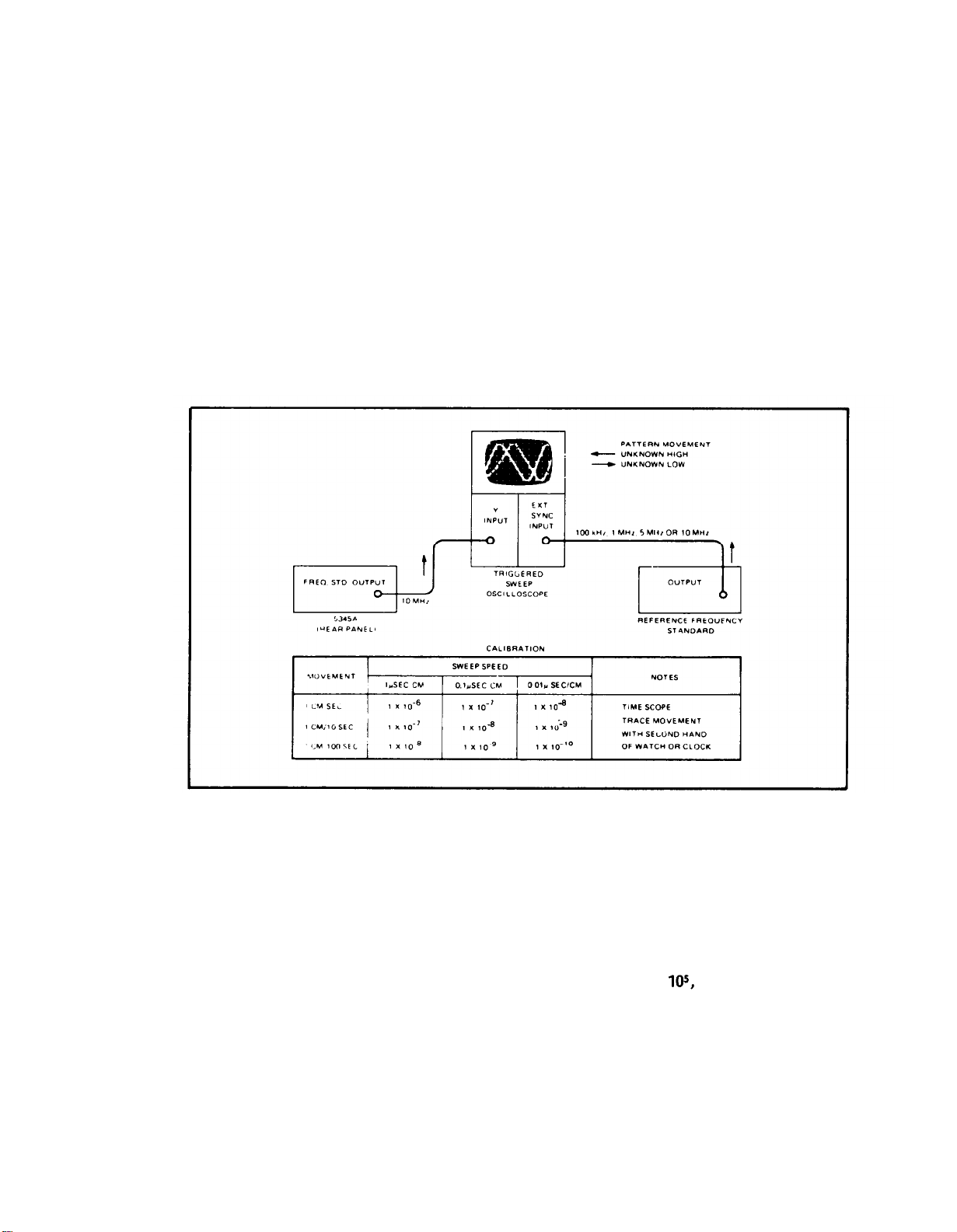
Model 5328A
Maintenance
5-22. ADJUSTMENTS
5-23. Adjustment procedures are provided for the oscillator and for the time interval unit
(sensitivity). The adjustments should not be done unless:
A trouble has been repaired which would affect these values.
a.
b. The instrument does not meet all specifications while performing the check in Table 5-4
(Performance Test), or during periodic calibration.
5-24. OSCILLATOR ADJUSTMENT. Periodically, the oscillator should be checked against a house
standard. When adjustment is required, use the oscilloscope method shown in Figure 5–2.
Using the appropriate sweep speed, adjust the oscillator until the movement of the pattern is
stopped or nearly stopped.
NOTE
When adjusting the 5328A oscillator, adjust FREQ ADJ on the 10544A
crystal oscillator unit, and the fine tuning adjustment A3R14.
Figure 5-1. 10 MHz Oscillator Frequency Check
5-25. Sensitivity Adjustments
1.
Adjust the channels A and B sensitivity as follows:
a.
Remove top cover of 5328A to gain access to variable resistors R28 and R26 on
the A12 Amplifier Assembly (see location photo in Section VIII),
b. Set 5328A front panel controls as follows:
FUNCTION
RESOLUTION
SLOPE (A) . . . . . . . . . . . . . . . . . . . . . . . . . . . . . . . . . . . . . . . . . . . . . .+
AC/DC (A) . . . . . . . . . . . . . . . . . . . . . . . . . . . . . . . . . . . . . . . . . . . DC
ATTEN (A)
LEVEL (A)
SEP-COM A
SAMPLE RATE . . . . . . . . . . . . . . . . . . . . . . . . . . . . . . . .
. . . . . . . . . . . . . . . . . . . . . . . . . . . . . . . . . . . . . . FREQ A
. . . . . . . . . . . . . . . . . . . . . . . . . . . . . . . . . . . . . . . . . . . .
. . . . . . . . . . . . . . . . . . . . . . . . . . . . . . . . . . . . . . . . .
. . . . . . . . . . . . . . . . . . . . . . . . . . . . . . . . .
. . . . . . . . . . . . . . . . . . . . . . . . . . . . . . . . . . . . . . . . .
lIY,
10 Hz
PRESET
SEP
MIDRANGE
1
5-19
Page 91

Model 5328A
Maintenance
c.
Set 5328A rear panel control as follows:
ARM . . . . . . . . . .
d.
Connect HP 608E Signal Generator (or equivalent) to INPUT A. Set signal gen-
erator to 35 MHz at 50 mV rms (140 mV p-p).
e.
Slowly decrease the signal generators output level to 15 mV rms (42 mV p-p),
while adjusting variable resistor R26, to obtain a stable correct display, on the
counter.
f.
To set Channel B sensitivity change 5328A front panel controls as follows:
FUNCTION . . . .
RESOLUTION . .
SEP-COM A
LEVEL B
With HP 651B Test Oscillator (set to 10 MHz at 100 mV rms) connected to lN-
g.
PUT A, connect a second signal generator (set to 40 MHz at 50 mV rms) to iN-
PUT B.
h.
Repeat step e adjusting variable resistor R28 instead of R26.
2.
Channel C Sensitivity adjustments:
Remove the top cover from the 5328A.
a.
b. Set signal to 100 MHz and reduce level until no stable reading in counter dis-
play. Adjust A8R82 for stable reading.
Repeat step b. until best sensitivity is obtained.
c.
. . . . . . . . . . . . . . . . . . . . . . . . . . . . . . . . . . . . . . . . . .
. . . . . . . . . . . . . . . . . . . . . . . . . . . . . . . . . . . . . . . . . . .
1(33
10 kHz
OFF
PRESET
. . . . . . . . . . . . . . . . . . . . . . . . . . . . . . . . . . . . .
. . . . . . . . . . . . . . . . . . . . . . . . . . . . . .
. . . . . . . . . . . . . . . . . . . . . . . . . . . . . . .
RATIO B/A
SEP
d. Repeat step b. to ensure that the counter still meets the requirement.
High Frequency Offset adjustments:
3.
Remove top cover.
a.
b. Set signal generator to 500 MHz and reduce signal level until display reading
is no longer stable. Adjust A8R85 until display is stable.
Repeat step b. until best balance is obtained.
c.
D-to-A Converter Adjustment procedure:
4.
The following adjustment procedure adjusts the All D-to-A Converter outputs for accurate
programmed trigger levels. Measuring the DAC outputs with a DVM is NOT an equivalent
procedure. Since the gain through the 5328A input amplifiers is not exactly equal to 1.00,
the signal arriving at the A12U4 comparator is not identical to the signal at the counter’s
input. As an example, assume the input amplifier gain is 0.95. Further assume an input signal
which goes from 0 volts to 1.0 volt and it is desired to trigger at the 1.0 volt level. Since the
signal arriving at A12U4 goes from 0 volts to 0.95 volts (due to the gain of 0.95), the trigger
level specified by the DAC to A12U4 must be 0.95 volts. Triggering at 0.95 volts on the A12U4
input signal is the same as triggering at the 1.0 volt level on the original signal. The procedure
described in the following takes into account the fact that the input amplifier gain is less
than 1.0.
The procedure offsets an input signal to the 5328A by 0, +2, and -2 volts and programs the
A and B channel trigger levels for 0, +2, and -2 volts respectively. For each offset, adjustments
are made by observing the A (and B) channel marker outputs and adjusting for a 50% duty
cycle. A 50% duty cycle indicates that the programmed trigger level (which is the center of
the hysteresis band) is exactly equal to the dc offset at the signal input to the A12U4
comparator.
5-20
Page 92

It is very important that the DAC adjustments be performed after the A and B channels
sensitivity adjustment. In this adjustment, follow the procedure outlined on page 12 of
the Option 041 Manual but adjust for optimum sensitivity by continuing to decrease the
signal generator level below 25 mV rms and adjusting the A12R26, R28 for stable counter
displays.
Set up the equipment as in Figure 5-2. Set the rear panel address switches on the 5328A to:
a.
Set the 651B test oscillator to 20kHz at a level of 25 mV rms (70mV p-p). Set the 180A oscil-
Ioscope A channel for ac coupling and 50 mV per division. Verify that the 20 kHz signal
into the counter is 70 mV p-p.
Model 5328A
Maintenance
b.
Disconnect the dc supply for a 0.0-volt dc offset on the input signal. Execute from the keyboard of the 9825A the following:
wrt
701,
“PF4G5S1S3A379+000*B37+000*R”
Monitoring the 5328A Marker A output on the oscilloscope, adjust A11R21 for a 50% duty
cycle in the Marker A signal as shown:
c.
Connect the 5328A B Marker output to the B channel of the oscilloscope. Adjust A11R20
for a 50% duty cycle in the Marker B output signal. (The counter has been programmed
for COMA.)
d.
Connect power supply as in the figure and adjust for a dc level of 2.00 volts (±2 mV) as
read on the DVM.
e.
Execute the following from the keyboard of the 9825A:
wrt
701,
“PF4G5S1S3A379+200*B37+200*R”
(press RECALL on 9825A and simply change DAC voltages as required.)
Adjust A11R18 for a 50% duty cycle on the 5328A B Marker output signal.
Connect the 5328A marker output signal to channel B of the oscilloscope. Adjust A11R24
for a 50% duty cycle on the A Marker output signal.
h.
Reconfigure dc power supply for negative voltages and set the voltage for -2.00 volts
(±2 mv)
i.
Execute the following from the keyboard of the 9825A:
o
wrt
7Ø1,
“PF4C5S1S3A379-200*B37-200*R”
Adjust All R26 for a 50% duty cycle on the A Marker output signal.
j.
k.
Connect the 5328A B Marker output to the B channel of the oscilloscope. Adjust A11R17
for a 50% duty cycle on the B Marker output signal.
5-21
Page 93
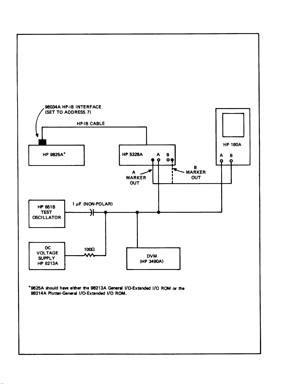
Model 5328A
Maintenance
5-22
Figure 5-2. DAC Adjustment Equipment Connections
Page 94

Model 5328A
Maintenance
Figure 5-3. DAC Adjustment oscilloscope readout and adjustment locations
5-23
Page 95
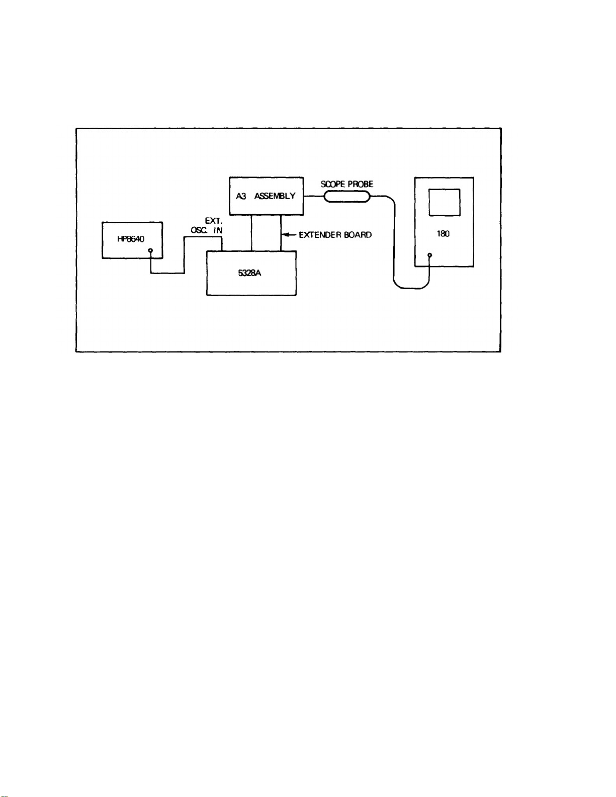
Model 5328A
Maintenance
5-26. Adjustment of A3 Oscillator Support
1. Connect 5328A, HP 8640, and HP 180 as shown in Figure 5-4.
Figure 5-4. Hookup For A3 Oscillator Support Adjustment
2. Place A3 on an extender board,
3. Apply a 1 MHz signal at a level greater than 1V rms to the 5328A rear-panel EXT OSC IN.
4. With scope probe, monitor A3U2 (6) non-component side of A3 circuit board.
5. Adjust A3C15 and A3C12 to minimize side-jitter in trace, as shown in Figure 5--5.
6. Put the scope in X10 and fine-tune the adjustments for minimum jitter.
5-27. TROUBLESHOOTING
5-28. Trouble isolation can best be accomplished by obtaining all possible information from the
controls, connectors, and indicators on the 5328A. This information should then be analyzed by
conducting the Performance Test (Table 5-4) to aid in determining symptoms of the trouble.
Troubleshooting aids are described in the following paragraphs,
5-29. TROUBLESHOOTING AIDS
5-30. Troubleshooting flowcharts for each assembly of the 5328A are provided at the back of
this section. Extender boards and test cards are available as service kits. This section contains
a table for analysis of functional signals and a table for IC troubleshooting.
5-24
5-31. Extender Board (05328-62016)
5-32. Two of these extender boards are supplied with the
Selector Assembly or the A8 Frequency C Assembly. One of
to extend the A10 assembly for the standard 5328A.
5328A to extend the A4 Function
these extender boards is required
Page 96

Model 5328A
Maintenance
Figure 5-5. A3 Jittler Adjustment
5-25
Page 97

Model 5328A
Maintenance
5-33. IC Troubleshooting
5-34. To troubleshoot the IC’s on the A1 Motherboard, proceed as follows:
a.
b. Set the FREQ RESOLUTION, N switch to 1 MHz, 1.
c.
d. Apply power and check for the logic states as shown in Table 5-5, using an HP Model
5-35. Function Signals
5-36. Table 5-6 lists the functional signals at pertinent points for each position of the FUNCTION switch. This information can be used to isolate problems that may occur in any of the
various modes of operation.
Set the FUNCTION switch to CHECK.
Remove top cover and remove A4 Function Selector Assembly.
10528A Logic Clip or a Model 10525T Logic Probe. A dark pattern indicates a logic high.
5-26
Page 98
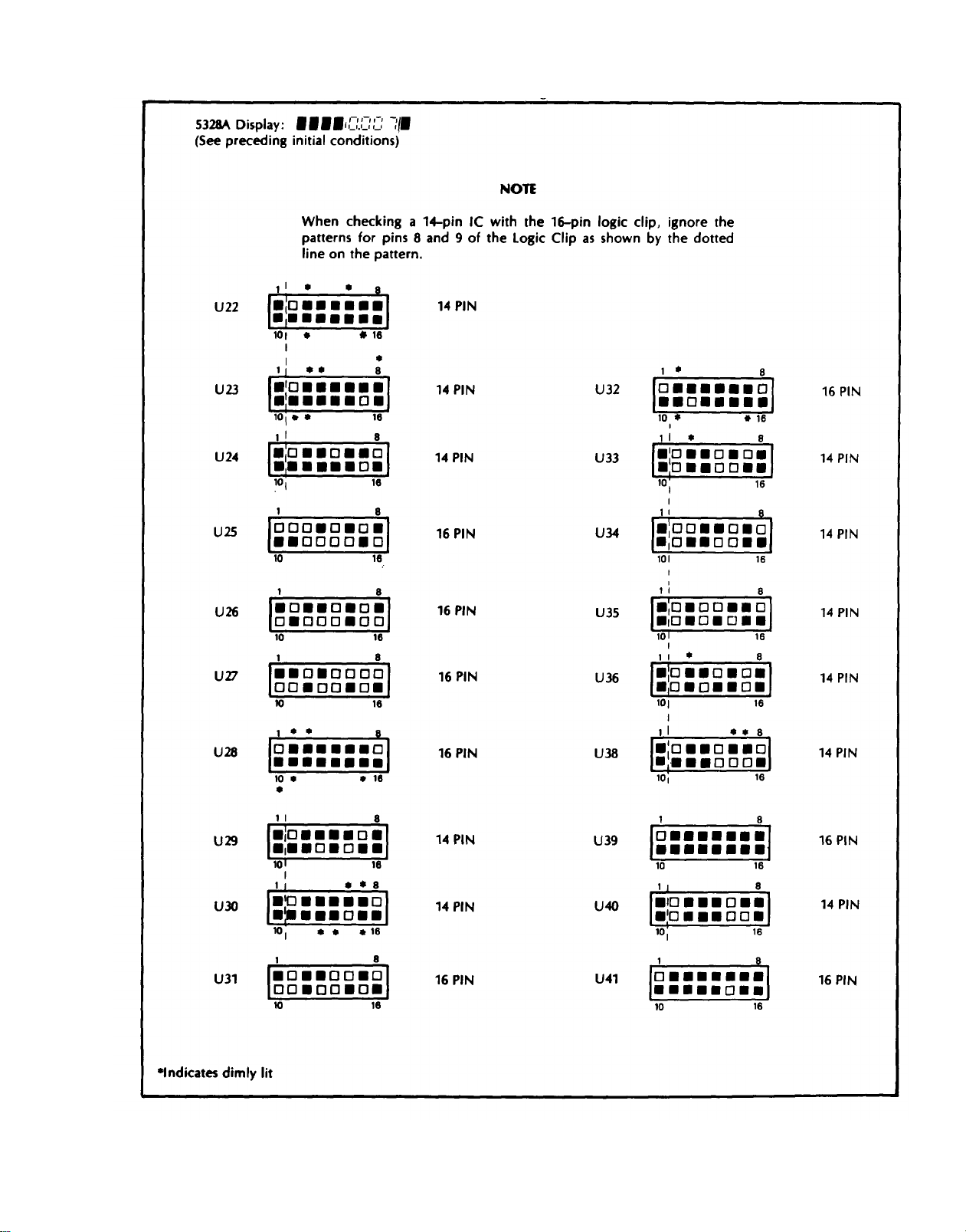
Table 5-5 IC Troubleshooting, A1 Motherboard
Model 5328A
Maintenance
5-27
Page 99

Model 5328A
Maintenance
Table 5-5. IC Troubleshooting, A1 Motherboard (Continued)
5-28
Page 100

Table 5-5. IC Troubleshooting, A1 Motherboard (Continued)
Model 5328A
Maintenance
5-29
 Loading...