

Page 1
HP L1702/FP7317 Service Manual
Page 1 of 143
SERVICE MANUAL
17” LCD Monitor
HP Compaq
L1702 Model F7317 Model
THESE DOCUMENTS ARE FOR REPAIR SERVICE INFORMATION ONLY. EVERY
REASONABLE EFFORT HAS BEEN MADE TO ENSURE THE ACCURACY OF THIS MANUAL; WE
CANNOT GUARANTEE THE ACCURACY OF THIS INFORMATION AFTER THE DATE OF
PUBLICATION AND DISCLAIMS RELIABILITY FOR CHANGES, ERRORS OR OMISSIONS.
MANUFACTURE DATA : Jan-12-2004
Update DATA: Jun-10-2004
Page 2
HP L1702/FP7317 Service Manual
Page 2 of 143
Table of Contents
Table of Contents ---------------------------------------------------------------------------------- 02
Revision List ---------------------------------------------------------------------------------------- 04
1.Configurations ---------------------------------------------------------------------05
2.Product Feature ---------------------------------------------------------------------05
3. LCD Monitor Description ---------------------------------------------------------------06
4. Operation Instructions --------------------------------------------------------------------07
4.1 General Instructions ------------------------------------------------------------------07
4.2 Control Button -------------------------------------------------------------------------07
4.3 Adjusting The Picture ----------------------------------------------------------------08
5. Input/Output Specification ------------------------------------------------------------------ 09
5.1 Input Signal Connector ------------------------------------------------------------------09
5.1.1 Analog D-SUB Connector -------------------------------------------------------09
5.2 Factory Preset Display Modes --------------------------------------------------------10
5.3 Power Supply Requirements ----------------------------------------------------------10
5.3.1 Input/Output Requirements ------------------------------------------------------10
5.3.2 Inverter Max Brightness -----------------------------------------------------------11
5.3.3 Inverter Min Brightness ------------------------------------------------------------11
5.4 Panel Specification (AU EN05/QDI L07/Hydis E13-100/LG E01) ---------12
5.4.1 Panel Feature ---------------------------------------------------------------------12
5.4.2 Display Characteristics ------------------------------------------------------------13
5.4.3 Optical Characteristics -----------------------------------------------------------15
5.4.4 Parameter guide line for CCFL Inverter --------------------------------19
6. Block Diagram -----------------------------------------------------------------------------------20
Page 3

HP L1702/FP7317 Service Manual
Page 3 of 143
6.1 Monitor Exploded View ----------------------------------------------------------------20
6.2 Software Flow Chart ---------------------------------------------------------------------22
6.3 Electrical Block Diagram ----------------------------------------------------------------23
6.3.1 Scalar Board ----------------------------------------------------------------------23
6.3.2 Inverter/Power Board -----------------------------------------------------------24
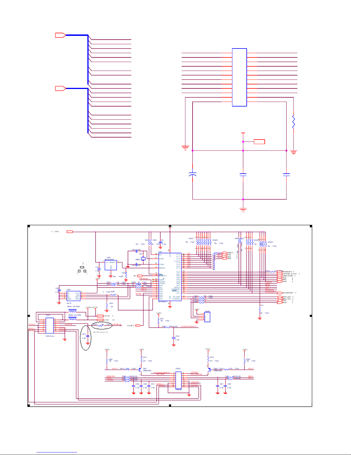
7. Schematic -----------------------------------------------------------------------------------------26
7.1 Scalar Board ----------------------------------------------------------------------------26
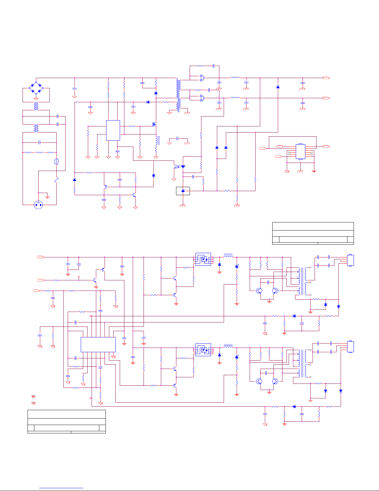
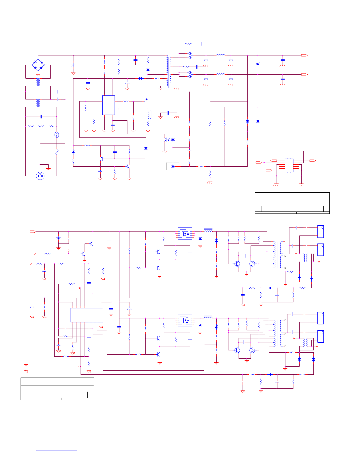
7.2 Inverter/Power Board --------------------------------------------------------------29
7.3 Key Pad Board -------------------------------------------------------------------------31
7.4 Audio Board ---------------------------------------------------------------------------32
8. PCB Layout --------------------------------------------------------------------------------------33
8.1 Main Board -----------------------------------------------------------------------------33
8.2 Inverter/Power Board ----------------------------------------------------------------34
8.3 Keypad Board -------------------------------------------------------------------------36
8.4 Audio Board ---------------------------------------------------------------------------37
9. Maintainability -----------------------------------------------------------------------------------37
9.1 Equipments and Tools Requirements ---------------------------------------------37
9.2 Trouble Shooting -----------------------------------------------------------------------38
9.2.1 Main Board -------------------------------------------------------------------38
9.2.2 Power/Inverter Board -------------------------------------------------------39
9.2.3 Key Pad Board -----------------------------------------------------------------41
10. White-Balance, Luminance Adjustment ----------------------------------------------- 42
11. EDID Content -----------------------------------------------------------------------------------43
12. BOM List ---------------------------------------------------------------------------------44~143
Page 4
HP L1702/FP7317 Service Manual
Page 4 of 143
12.1 L1702 Model ---------------------------------------------------------------------44~75
12.2 F7317 Model --------------------------------------------------------------------75~107
12.3 LG Panel Model --------------------------------------------------------------108~125
12.4 Hydis Panel Model -----------------------------------------------------------125~143
Revision List
Revision Date Change Description
V1.0 Jan-12 Initial Release
V2.0 Jun-10 Add Panel Spec and BOM of LG & Hydis panel model
Update the BOM list of AU Panel model
Page 5
HP L1702/FP7317 Service Manual
Page 5 of 143
1.CONFIGURATIONS
The configurations information in this section is provided for reference only. Consult the SKU
Matrix for each kit (typically a boxed monitor assembly with cushions, power cord, etc.)
MODEL BRANDING COLORS SPEAKERS BEZEL EDID #
FP7317
Compaq
Consumer
Compaq Silver
Carbon
Yes FP7317 CPQ 145B
F1723
HP
Consumer
Platinum Blue
Dusk Lake
Yes f1723 HWP 2609
VF17 HP CTO
Platinum Blue
Dusk Lake
No vf17 HWP 260A
FP17
Compaq
CTO
Compaq Silver
Carbon
No FP17 CPQ 145E
L1702
HP
Commercial
Compaq Silver
Carbonite
No 1702 HWP 2601
L1702m
HP
Commercial
Compaq Silver
Carbonite
Yes 1702m HWP 2601
L1702C
HP
Commercial
Carbonite No 1702 HWP 2601
2. PRODUCT FEATURE
43.2cm(17”) a-si TFT Active matrix LCD panel, 0.264mm dot pitch
Scalar chipset MST9151B
16 factory presets, 20 new modes
Vertical refresh rate 55Hz to 75Hz; Horizontal frequency 30kHz to 83kHz
Power Internal AC 100V-240V(+/-10%)
Tilt -5 ° to 20 °
CE mark
TCO 99 mark
VESA DPMS compliant
VESA DDC2B compliant
Page 6
HP L1702/FP7317 Service Manual
Page 6 of 143
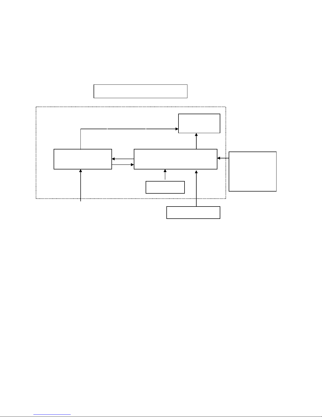
3. LCD MONITOR DESCRIPTION
The LCD Monitor will contain main board, power board, key board and which house the flat panel control
logic, brightness control logic and DDC.
The power board will provide AC to DC Inverter voltage to drive the backlight of panel and the main
board chips each voltage.
Power Board
Flat Panel and
CCFL backlight
Main Board
Keyboard
RS232 Connector
For white balance
adjustment in
factory mode
HOST Computer
CCFT Drive.
AC-IN
90V-264V
Video signal, DDC
Monitor Block Diagram
Page 7
HP L1702/FP7317 Service Manual
Page 7 of 143
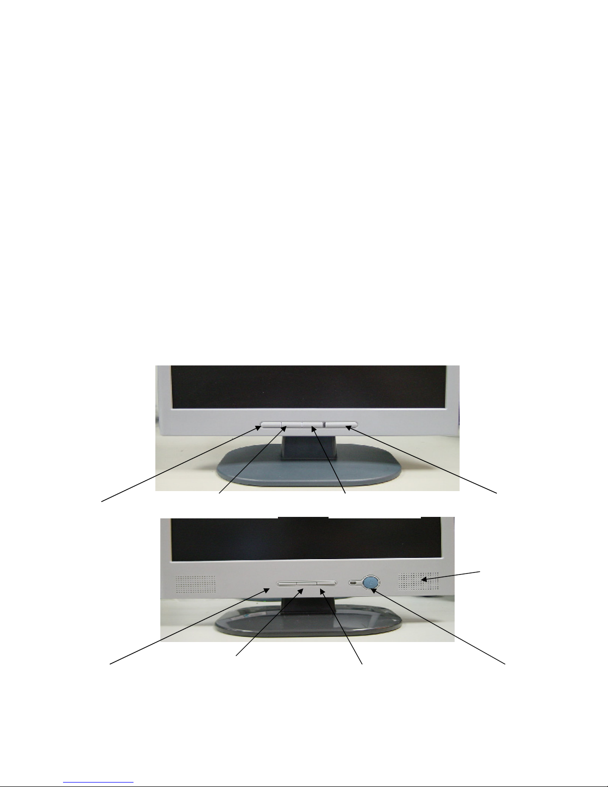
4. OPERATION INSTRUCTIONS
4.1 General Instructions
Press the power button to turn the monitor on or off. The other control buttons are located
at front panel of the monitor. By changing these settings, the picture can be adjusted
to your personal performance.
-
The power cord should be connected and insert to adaptor.
-
Connect the video cable from the monitor to the computer VGA card.
-
Press the power button to turn on the monitor, the power indicator will light up to Green.
4.2 Control Buttons
- Power Button:
When pressed, the monitor enters the off mode, and the LED turns blank. Press again to restore
normal status.
- (Down/ Auto) and + (Up) Button:
The -/+ Button is browse OSD key. Press a select into adjustment.
The Auto Adjust Key is used to automatically set the H Position, V Position, Clock and Phase.
- Select Key:
Select key is into OSD sub-menu hot key when OSD turn on.
- Power Indicator:
Green — Power On mode.
Amber — Power Saving mode.
Blank — Power Off Mode.
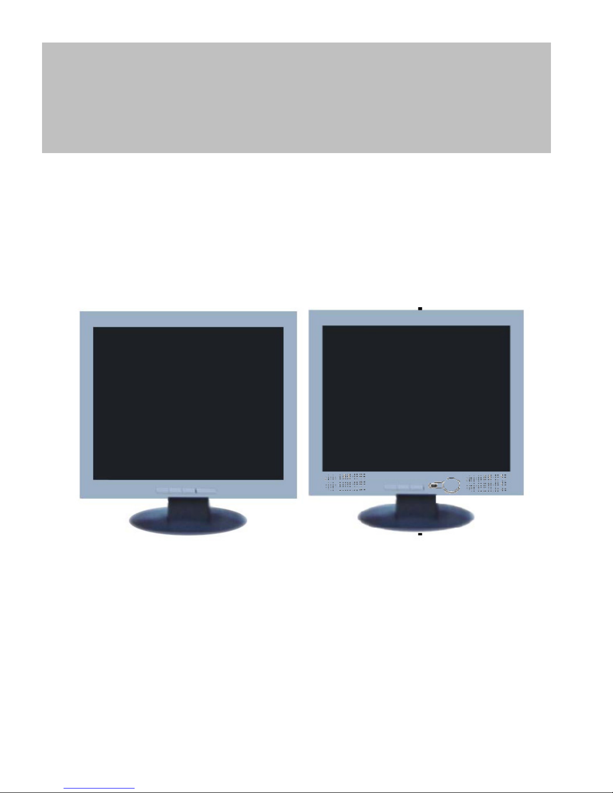
CONTROL BUTTONS
Select Button Down / Auto Button Up Button On/Off Switch
Speaker
Select Button Down / Auto Button Up Button On/Off Switch
Model:
L1702
Model:
F7317
Page 8
HP L1702/FP7317 Service Manual
Page 8 of 143
4.3 Adjust The Picture
1.
Brightness
Adjust the brightness.
2.
Contrast Adjust the contrast
3.
Image Control
Adjust the:
z Auto Adjustment: Adjusts the main settings and produces a
stable, centered image.
z H-Position: horizontal position of the screen image.
z V-Position: vertical position of the screen image.
z Clock: frequency of the pixel clock to minimize vertical bar.
z Phase: phase value to minimize horizontal jitters.
3.
Color
z 9300K: recall 9300K color
z 6500K-sRGB: recall 6500K sRGB color
z Custom Color: adjusts the color tint of white, and the red,
green, and blue (RGB) mix for colors.
4.
Language Shows the language of the OSD window.
5.
Management
z Power Saver: enable/disable power saving
z Power On Recall: enable/disable power recall
z Mode Display: enable/disable mode display
z Sleep Timer: set sleep timer
z Basic Menu: set to basic menu
6.
OSD Control
OSD (on Screen Display) settings: adjusts the H/V position,
timeout, On Screen Display window.
7.
Factory Reset
Resets the display to original factory settings for color, brightness,
phase, and clock.
8.
Exit Closes the OSD window.
Page 9
HP L1702/FP7317 Service Manual
Page 9 of 143
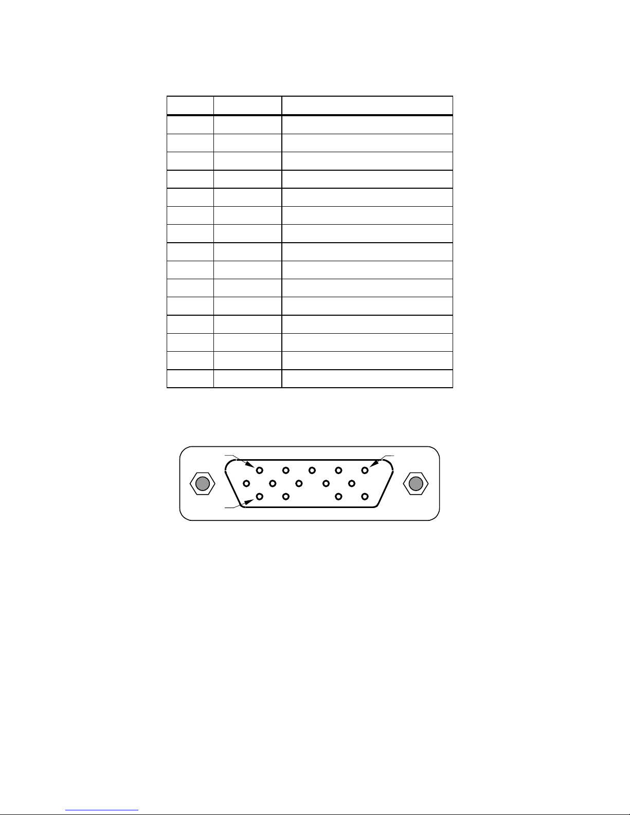
5. Input/Output Specification
5.1 Input Signal Connector
5.1.1 Analog D-SUB Connector
PIN MNEMONIC SIGNAL
1 RV Red Video
2 GV Green Video
3 BV Blue Video
4 NC
None
5 GND Ground (DDC Return)
6 RG Red GND
7 GG Green GND
8 BG Blue GND
9 +5 V +5 V (from PC)
10 SG Sync Ground
11 NC None
12 SDA DDC Data
13 HS Horizontal Sync
14 VS Vertical Sync
15 SCL DDC Clock
VGA connector layout
PIN 1
PIN 5
PIN 11
Page 10
HP L1702/FP7317 Service Manual
Page 10 of 143
5.2 Factory Preset Display Modes
Preset
Pixel
Format
Horz
Freq (KHz)
Horz
Polarity
Vert Freq
(Hz)
Vert
Polarity
Pixel Clk
(MHz)
Source
1 640 x 480 31.469 - 59.940 - 25.175 VGA
2 640 x 480 37.861 - 72.809 - 31.500 VESA
3 640 x 480 37.500 - 75.000 - 31.500 VESA
4 720 x 400 31.469 - 70.087 + 28.322 VGA
5 800 x 600 37.879
+
60.317 + 40.000 VESA
6 800 x 600 48.077 + 72.188 + 50.000 VESA
7 800 x 600 46.875 + 75.000 + 49.500 VESA
8 832 x 624 49.726 ± 74.551 ± 57.284 MAC
9 1024 x 768 48.363 - 60.004 - 65.000 VESA
10 1024 x 768 56.476 - 70.069 - 75.000 VESA
11 1024 x 768 60.023 + 75.029 + 78.750 VESA
12 1152 x 870 68.68 - 75.06 - 100.000 Mac
13 1152 x 900 71.71 - 76.05 - 105.561 Sun
14 1280 x 1024 63.98 + 60.02 + 108.000 VESA
15 1280 x 1024 79.97 + 75.02 + 135.000 VESA
5.3 Power Supply Requirements
5.3.1 Input / Output Requirements
PARAMETER RANGE
AC Input Voltage 90 to 264V
AC Input Frequency 47 to 63 Hz
AC Input Current 1.5A MAX
Inrush Current 60A MAX AT 264VAC COLD START
Leakage Current 3.5 mA MAX and less than 0.25mA at 100Vac
Output voltage / current 12V / 2.5A , 5V / 2A
Output power 45W Max
Efficiency >80%
Saving Mode <2W Max @5V/0.1A , 12V/0A
Page 11
HP L1702/FP7317 Service Manual
Page 11 of 143
5.3.2 Inverter Max Brightness
(Vadj:4.5v), LOAD=100KΩX4 (ROOM TEMPERATURE 25℃ ±4℃)
PWPC1742AUH1
ITEM SYMBOL MIN. TYP. MAX. UNIT REMARK
Input voltage Vin 10.8 12 13.2 V ---
Input current Iin --- 2250 2500 mA FOR 4 LOAD
Output Current Iout 13.5 14.0 14.5 mA FOR 1 LOAD
Frequency F 50 55 60 KHZ FOR 1 LOAD
H.V Load Vload 600 700 800 Vrms
RL=100KΩ
Start voltage Vst 1450 1700 1800 Vrms RL=CCFL
Protect delay time PDT --- 1 Sec ---
PWPC1742QDH1
ITEM SYMBOL MIN. TYP. MAX. UNIT REMARK
Input voltage Vin 10.8 12 13.2 V
Input current Iin 2250 2500 mA FOR 4 LOAD
Output Current Iout 6.5 7.0 7.5 mA FOR 1 LOAD
Frequency F 50 55 60 KHZ FOR 1 LOAD
H.V Load Vload 625 725 825 Vrms
RL=100KΩ
Start voltage Vst 1450 1700 1800 Vrms RL=CCFL
Protect delay time PDT 1 Sec
5.3.3 Inverter Min Brightness
(Vadj:0.0v), LOAD=100KΩX4 (ROOM TEMPERATURE 25℃ ±4℃)
PWPC1742AUH1
ITEM SYMBOL MIN. TYP. MAX. UNIT REMARK
Input voltage Vin 10.8 12 13.2 V
Input current Iin 700 900 mA FOR 4 LOAD
Output Current Iout 3.0 3.5 4.0 mA FOR 1 LOAD
Frequency F
--- --- --- KHZ
---
Start voltage Vst
--- --- --- Vrms ---
H.V Load Vload
--- --- ---
Vrms
RL=100KΩ
Page 12
HP L1702/FP7317 Service Manual
Page 12 of 143
PWPC1742QDH1
ITEM SYMBOL MIN. TYP. MAX. UNIT REMARK
Input Voltage Vin 10.8 12 13.2 V
Input Current Iin 700 900 mA FOR 4 LOAD
Output Current Iout 3.0 3.5 4.0 mA FOR 1 LOAD
Frequency F
--- --- --- KHZ
Start Voltage Vst
--- --- --- Vrms
H.V Load Vload --- --- --- Vrms
RL=100KΩ
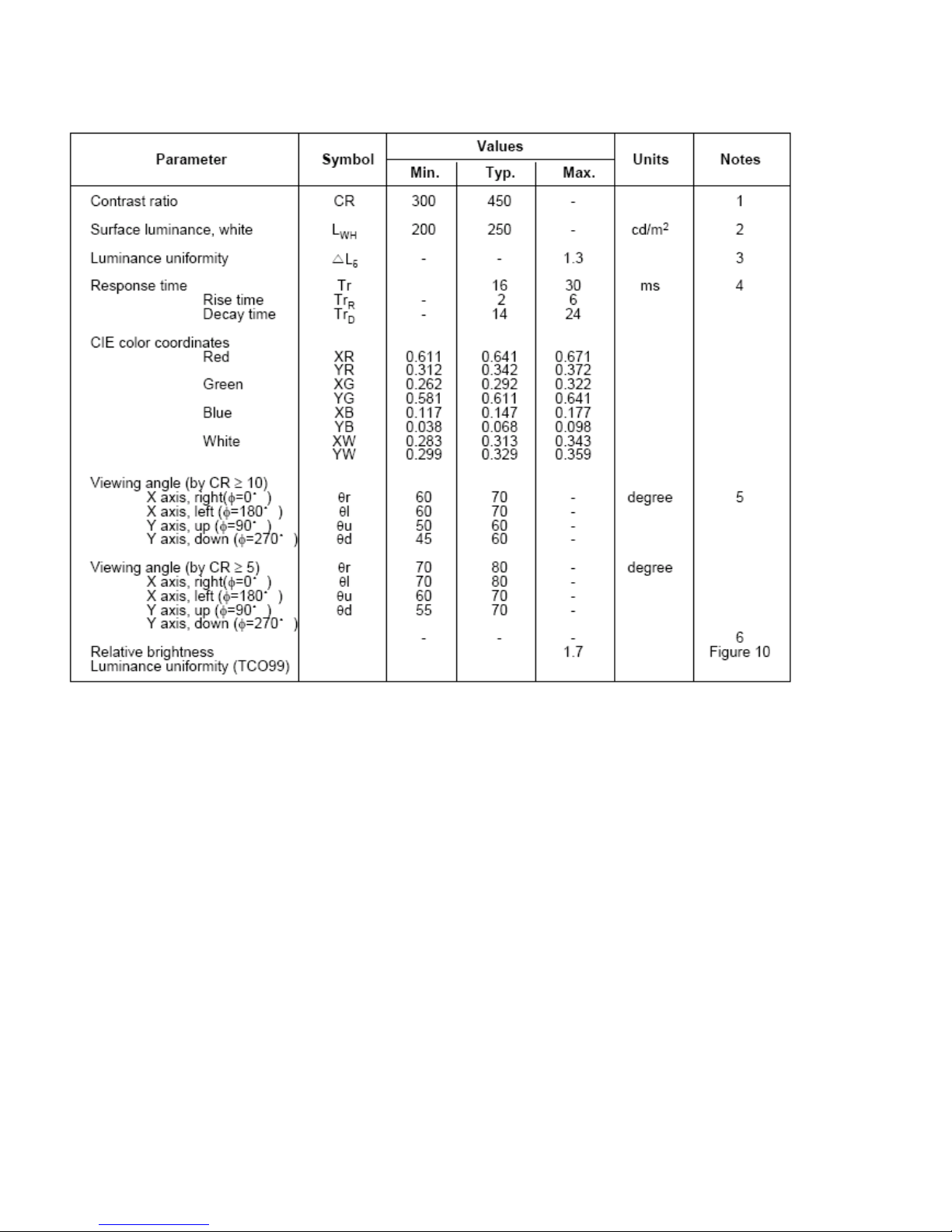
5.4 PANEL SPECIFICATION (AU EN05/ QDI L07/ Hydis E13-100/LG E01)
5.4.1 Panel Feature
AU EN05
–This specification applies to the 17.0 inch Color TFT-LCD Module M170EN05
–The display supports the SXGA (1280(H) x 1024(V)) screen format and 262k colors(RGB 6-bits data)
–All input signals are 2 Channel LVDS interface compatible
–This module does not contain an inverter card for backlight
QDI L07
–High aperture panel; high-brightness or low power consumption
–Brilliant and high contrast image
–Small footprint and thin shape
–SXGA resolution
–LVDS interface
–Low power consumption
–Wide viewing angle
Hydis E13-100
–LVDS interface with 2 pixels / clock
–High-speed response
–Lower power consumption
–6 bits(FRC) colors, display 16,194,227
–Incorporated edge type back-light(Four lamps)
–High luminance and contrast ratio, Lowe reflection and wide viewing angle
–DE(Data Enable) & H-Sync & V-Sync mode
LG E01
–This TFT-LCD has a 17.0 inch diagonal measured display area with SXGA resolution(1024 vertical
by 1280 horizontal pixel array)
–8-bit gray scale signal for each dot, thus, presenting a palette of more than 16.2M colors with FRC.
–Lowe power, high speed ,low EMI.
–Thin thickness, wide viewing angle, lower power are critical factors and graphic displays.
Page 13
HP L1702/FP7317 Service Manual
Page 13 of 143
5.4.2 Display Characteristics
AU EN05
ITEM UNIT SPECIFICATIONS
Screen Diagonal [mm] 432(17.0”)
Active Area [mm] 337.920(H) x 270.336(V)
Pixel Pitch H x V 1280(x3) x 1024
Pixel Arrangement [mm] 0.264(per one triad) x 0.264
Display Mode R.G.B Vertical Stripe
White Luminance (Center) [cd/m²] 260 cd/m²@7mA (Typ)
Contrast Ratio 450:1(Typ)
Optical Response Time [msec] 16(Typ)
Color saturation 72% NTSC
Nominal input Voltage VDD [Volt] +5.0V
Power consumption
(VDD line + CCFL line)
[Watt]
25W (Typ.) (w/o Inverter, All white pattern)
Weight [Grams] 2000(Typ)
Physical Size [mm] 358.5(W) x 296.5(H) x 19.0(D)(Typ)
Electrical Interface Even/Odd R/G/B data, 3 sync signal clock
Support Color 262K colors (RGB 6-bit data)
Temperature Range
Operating Storage (Shopping )
[℃]
[℃]
0 to +50
-20 to +60
QDI L07
PARAMETER SPECIFICATION UNIT
Display Size 43(17") Diagonal cm
Active area 337.9(H) x 270.3(V) mm
Pixel format
1280(H) x 1024(V) pixel
(1 Pixel=R+G+B dots)
Pixel pitch 0.264(H) x 0.264(V) mm
Pixel configuration R, G, B vertical stripe
Display mode Normally White
Unit outline dimensions (typ.)*1 358.5 x 296.5x 16.5 mm
weight 1970(Max.) g
Surface treatment
Anti-glare and hard-coating 3H
Low reflection (~ 5%)
Lamp Quantity
4 pcs
1.Note: Excluding backlight cables.
Page 14
HP L1702/FP7317 Service Manual
Page 14 of 143
Hydis E13-100
Parameter Specification Unit
Active area 337.92(H) x 270.336(V) mm
Number of pixels 1280(H) x1024(V) pixels
Pixel pitch 0.264(H) x 0264(V) mm
Pixel arrangement RGB Vertical stripe
Display colors 16,194,227 colors
Display mode Normally White
Dimensional
outlint
358.5(H)x 296.5(V)x 17.0(D)typ. mm
Weight 1900 max gram
Back-light Top/Bottom edge side 4-CCFL type Note1
LG E01
Active screen size 17.0 inch (43.27cm)diagonal
Outline Dimension 358.5(H)x296.5(V)x17.0(D)mm(Typ.)
Pixel Pitch 0.264mm x 0.264mm
Pixel Format 1280(H)x 1024(V)Pixels. RGB stripe arrangement
Display colors 16.2M colors
Luminance, white
250cd/㎡(Typ. Center 1 point)
Power Consumption 19.05 Watts(Typ.)
Weight 1890g(Typ.)
Display operating mode Transmissive mode, normally white
Surface treatments Hard coating(3H),Anti-glare treatment of the front polarizer
Page 15
HP L1702/FP7317 Service Manual
Page 15 of 143
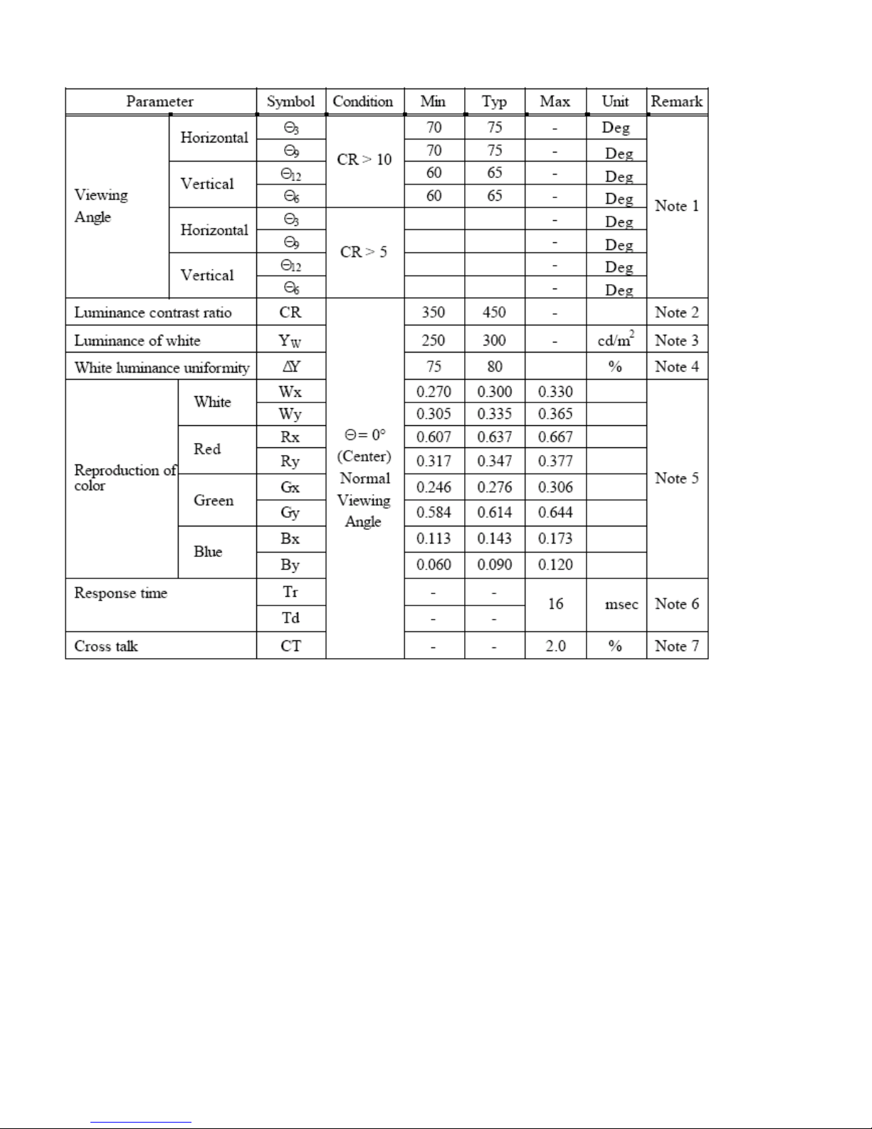
5.4.3 Optical Characteristics
QDI L07
Parameter Symbol Condition Min Typ. Max. Unit Remark
Viewing angle
range
Horizontal θ21, θ22
CR>10
65 75 Deg
Note1,4
Vertical
θ11 55 65 Deg
θ12 50 60 Deg
Horizontal θ21, θ22
CR>5
85 Deg
Vertical
θ11 75 Deg
θ12 70 Deg
Contrast ratio CR θ=0° 300 450 — Note2, 4
Response time t θ=0° — 20 ms
Note3, 4 Rise time tr 4 ms
Fall time td 16 ms
Chromaticity of White(CIE 1931)
Wx 0.283 0.313 0.343
Note4
Wy 0.299 0.329 0.359
Chromaticity of Red(CIE 1931)
Rx 0.603 0.633 0.663
Ry 0.306 0.336 0.366
hromaticity of Green(CIE 1931)
Gx 0.270 0.300 0.330
Gy 0.556 0.586 0.616
Chromaticity of Blue(CIE 1931)
Bx 0.116 0.146 0.176
By 0.073 0.103 0.133
Luminance of white
Note 4[Note 4]
YL 240 300
cd/㎡
IL=7.0
mArms
White Uniformity δw — 1.25 1.33 Note5
Cross talk 1.50% Note6
Page 16
HP L1702/FP7317 Service Manual
Page 16 of 143
AU EN05
The optical characteristics are measured under stable conditions at 25℃(Room Temperature):
ITEM UNIT CONDITIONS MIN TYP. MAX.
Viewing Angle
[degree]
Horizontal(Right)
CR=10(Left)
60
60
70
70
–
–
[degree]
[degree]
Vertical(Up)
CR=10(Down)
60
60
70
70
–
–
[degree]
[degree]
Horizontal(Right)
CR=5(Left)
70
70
80
80
–
–
[degree]
[degree]
Vertical(Up)
CR=5(Down)
70
70
80
80
–
–
[degree]
Contrast ratio Normal Direction 250 450 –
Response Time (Note 1)
[m sec] Raising Time – 4 5
[m sec] Falling Time – 12 20
[m sec] Raising +Falling – 16 25
Color /Chromaticity
Coordinates(CIE)
Red x 0.61 0.64 0.67
Red y 0.31 0.34 0.37
Green x 0.26 0.29 0.32
Green y 0.58 0.61 0.64
Blue x 0.11 0.14 0.17
Blue y 0.04 0.07 0.10
Color Coordinates (CIE) White
White x 0.28 0.31 0.34
White y 0.30 0.33 0.36
White Luminance
@CCFL 7.0mA (center)
[cd/㎡]
200 260 –
Luminance Uniformity(Note 2) [%] 75 80 –
TCO99 1.5.2B luminance
uniformity (Note 3)
1.7
Crosstalk (in 75Hz)(Note 4) [%] 1.5
Page 17
HP L1702/FP7317 Service Manual
Page 17 of 143
Hydis E13-100
Page 18
HP L1702/FP7317 Service Manual
Page 18 of 143
LG E01
Page 19
HP L1702/FP7317 Service Manual
Page 19 of 143
5.4.4 Parameter guide line for CCFL Inverter
Back-Light Unit:
AU EN05
SYMBOL PARAMETER MIN TYP MAX UNITS CONDITION
(L63) White Luminance 200 260 –
[cd/㎡] (Ta=25℃)
ISCFL CCFL standard current 6.5 7.0 7.5
[mA]
rms
(Ta=25℃)
IRCFL CCFL operation range 3.0 7.0 7.5
[mA]
rms
(Ta=25℃)
ICFL CCFL Inrush current – 26 34 [mA] Note 1
fCFL
CCFL Frequency 40 50 80 [KHz]
(Ta=25℃)
Note 2
ViCFL
(0℃)
CCFL ignition Voltage 1700
[Volt]
rms
(Ta=0℃)
Note 3
ViCFL
(25℃)
CCFL ignition Voltage 1200
[Volt]
rms
(Ta=25℃)
Note 3
TCFL CCFL Dark start time 1.0 sec
(Ta=25℃)
VCFL
CCFL Discharge Voltage
(Reference)
700 860
[Volt]
rms
(Ta=25℃)
Note 4
PCFL CCFL Power consumption 19.6 25.8 [Watt]
(Ta=25℃)
Note 4
QDI L07
The backlight system is an edge-lighting type with 2- CCFL(Cold Cathode Fluorescent Lamp).
The characteristics of four lamps are shown in the following tables.
PARAMETER SYMBOL MIN TYP MAX UNIT REMARK
Lamp current range IL 3.0 7.0 8.0 mArms Note1
Lamp voltage VL 725 Vrms
Lamp power consumption PL 5.1 W Note2 IL=7.0mA
Lamp frequency FL 52 kHz Note3
Established starting voltage Vs
1100 Vrms
Ta =2 5℃
Note4
1420 Vrms
Ta =0 ℃
Lamp life time LL 40000 50000 hour Note5
Page 20

HP L1702/FP7317 Service Manual
Page 20 of 143
6. Block Diagram
6.1 Monitor Exploded View
L1702 Model
Page 21
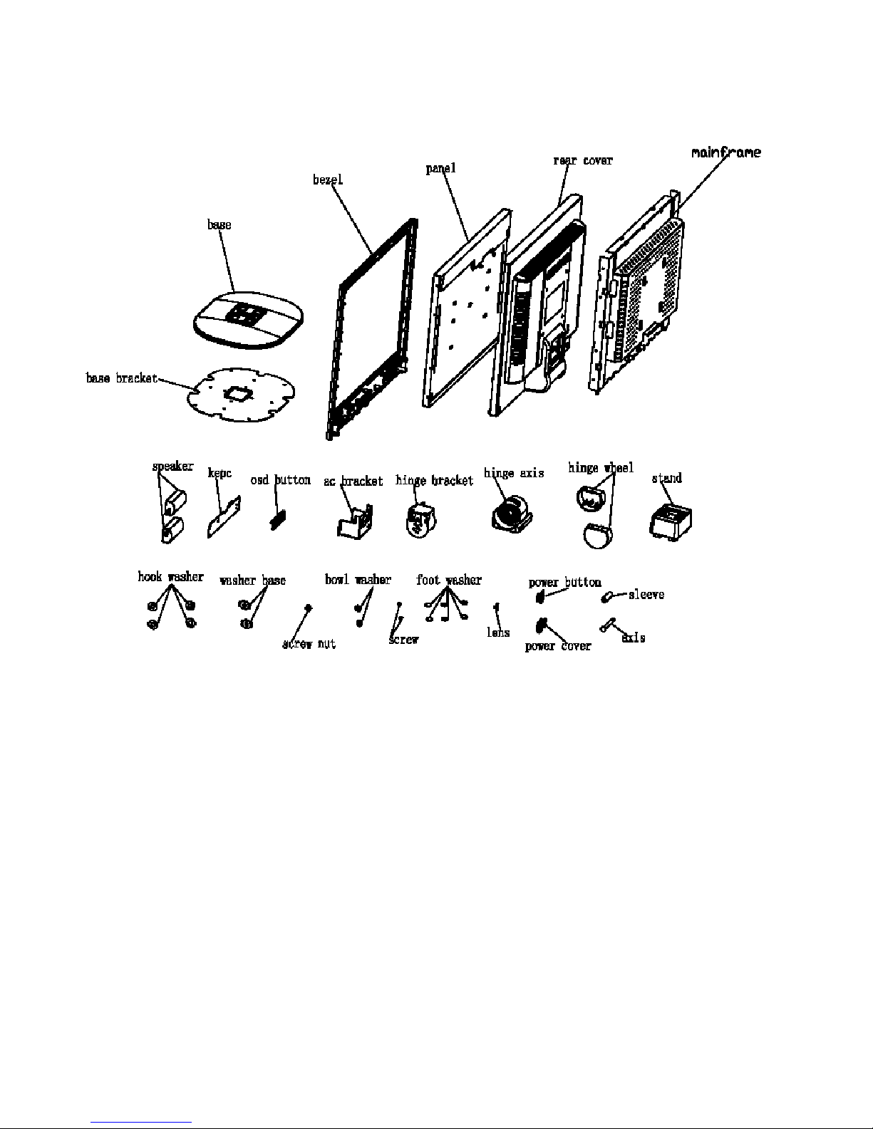
HP L1702/FP7317 Service Manual
Page 21 of 143
F7317 Model
Page 22
HP L1702/FP7317 Service Manual
Page 22 of 143
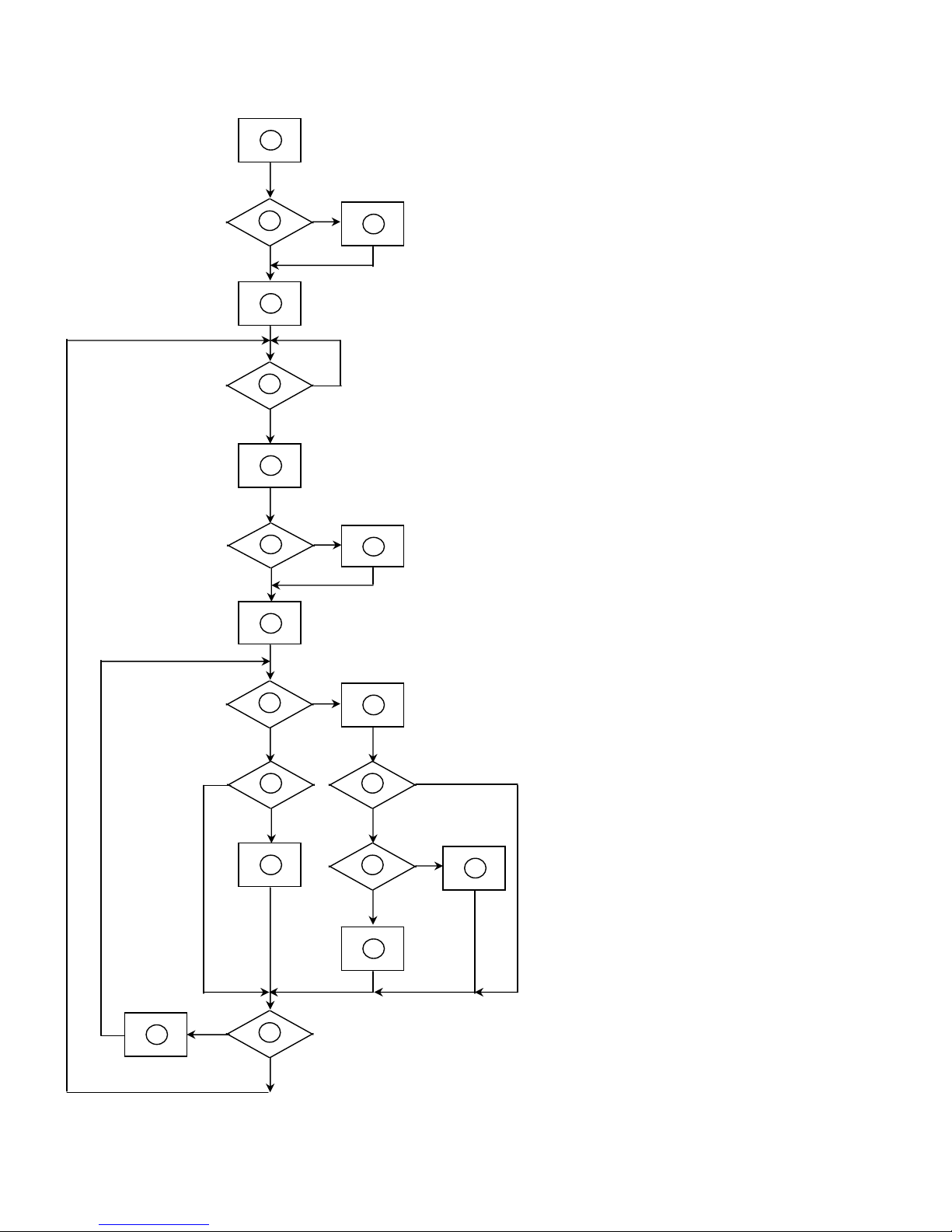
6.2 Software Flow Chart
1) MCU initialize.
2) Is the eeprom blank?
3) Program the eeprom by default values.
4) Get the PWM value of brightness from
eeprom. Check the pin PANEL1 and PANEL2
to tell which panel to get with it.
5) Is the power key pressed?
6) Clear all global flags.
7) Are the AUTO and SELECT keys pressed?
8) Enter factory mode.
9) Saving the power key status into eeprom.
Turn on the LED and set it to green color.
Scalar initializes.
10) In standby mode?
11) Update the lifetime of back light.
12) Check the analog and digital port, are there
any signals coming?
13) Does the scalar send out a interrupt request?
14) Wake up the scalar.
15) Are there any signals coming from analog or
digital port?
16) Display " No Input Signal " message. And go
into standby mode after the message
disappear.
17) Program the scalar to be able to show the
coming mode.
18) Process the OSD display.
19) Read the keyboard. Is the power key
pressed?
1
2
5
10
12
7
6 4 3
8
9 14 11
13
1
5
16
1
7
19
18
Page 23
HP L1702/FP7317 Service Manual
Page 23 of 143
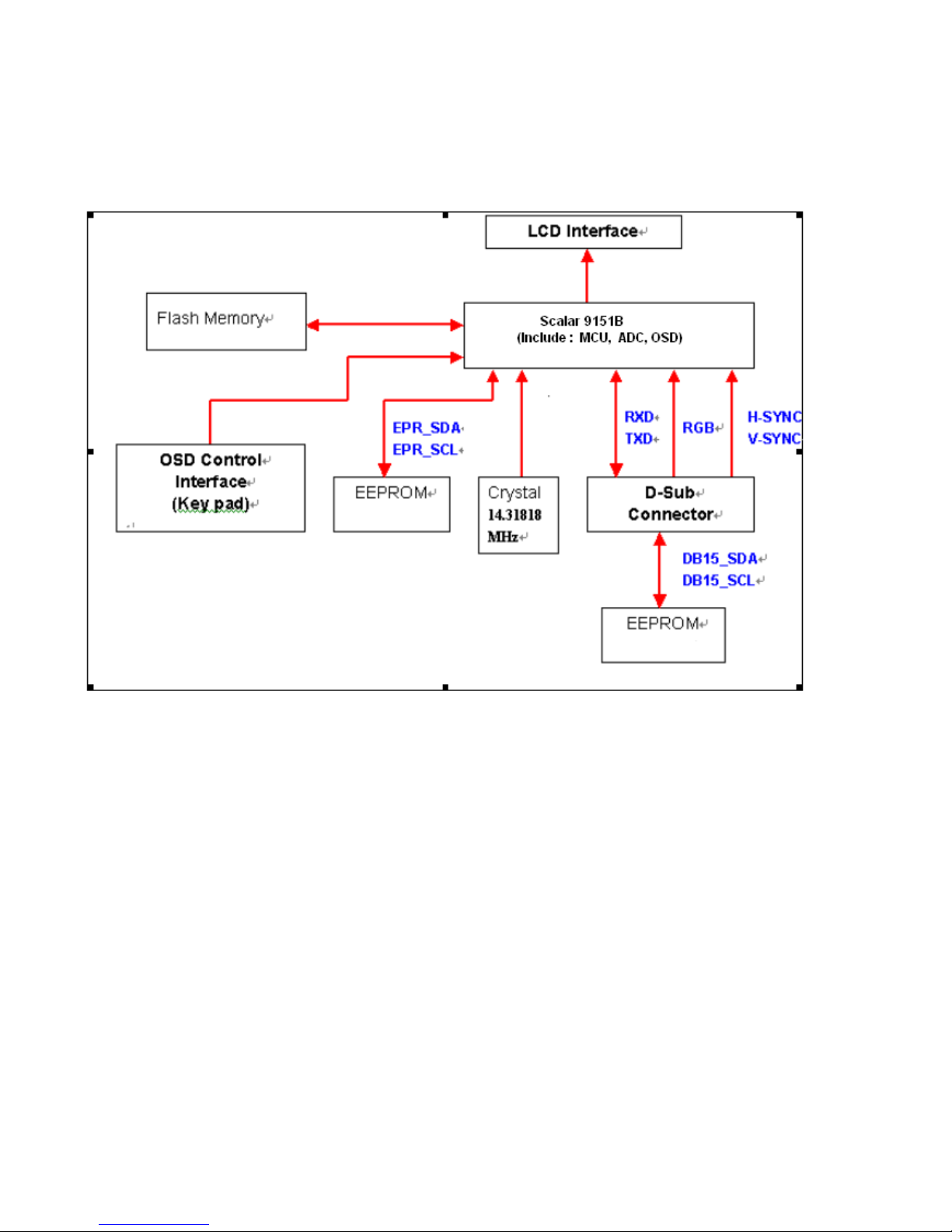
6.3 Electrical Block Diagram
6.3.1 Scalar Board Block Diagram
Page 24
HP L1702/FP7317 Service Manual
Page 24 of 143
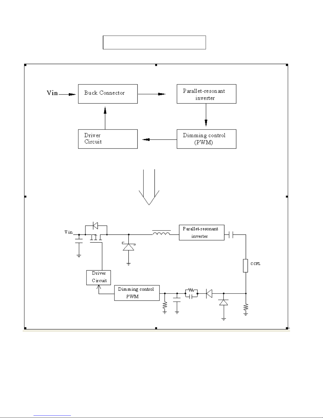
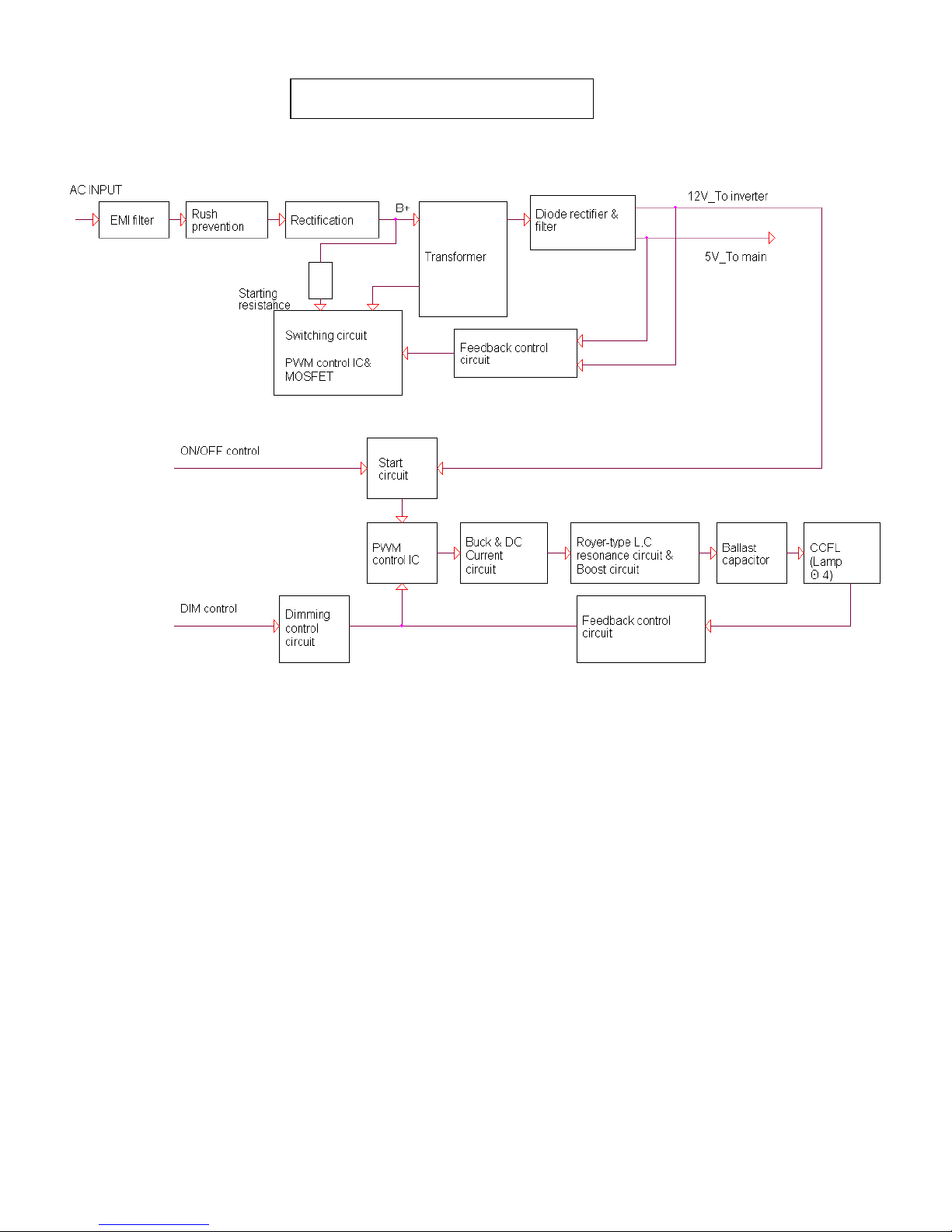
6.3.2 Inverter / Power Board Block Diagram
Inverter Block Diagram
Page 25
HP L1702/FP7317 Service Manual
Page 25 of 143
Power Block Diagram
Page 26

HP L1702/FP7317 Service Manual
Page 26 of 143
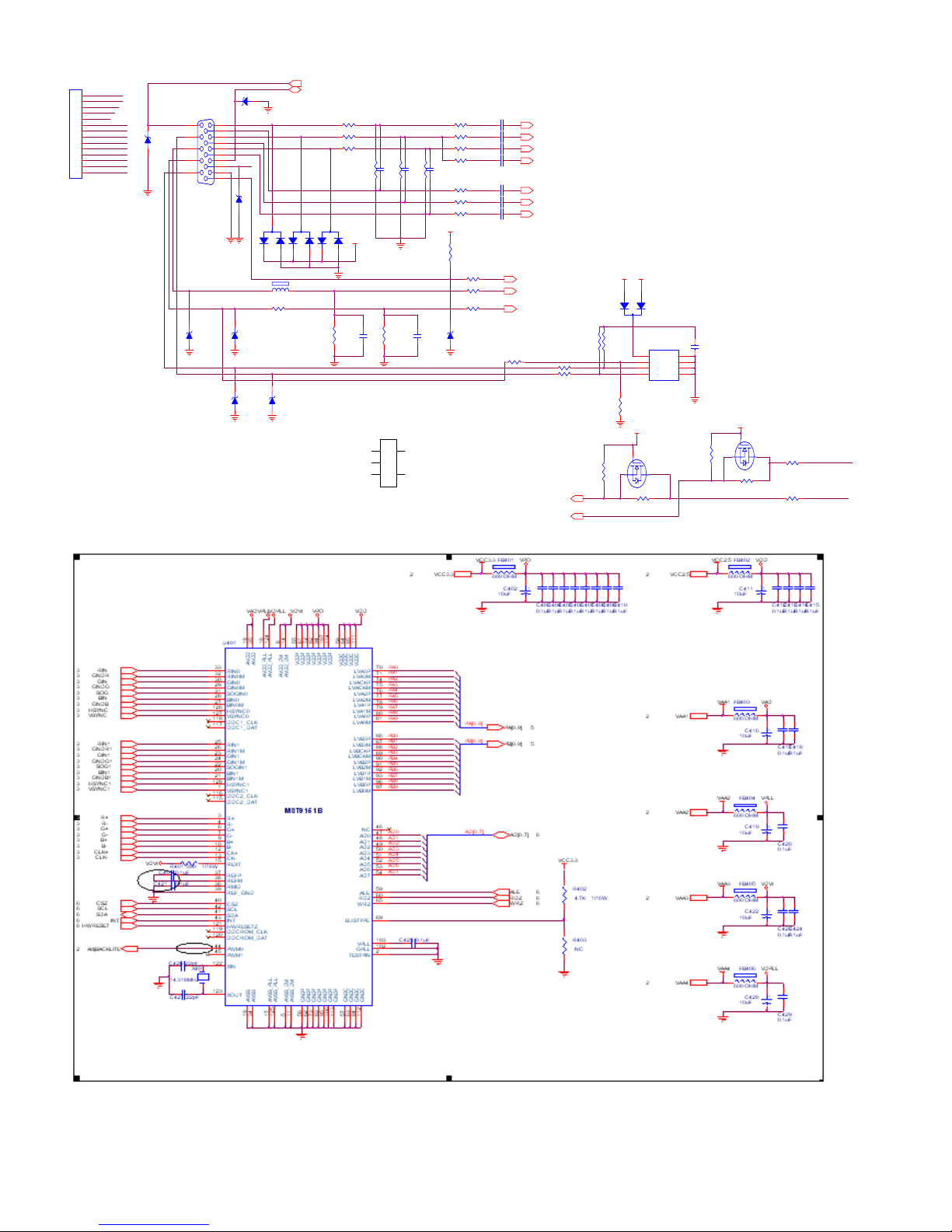
7.SCHEMATIC
7.1 SCALAR BOARD
R309 100 1/16W
VCC5V
R356
4.7K 1/16W
GNDG 4
R304 100 1/16W
VSYNC 4
D328
MLL5232B 5.6V
1
AG+
HSI-1
AG-
HSYNC 4
VCC5V
RXD
AB-
R307
75 1/16W
2
GIN 4
D303
BAV99
3
1
2
R301
75 1/16W
PC5V
3
R359
0 1/16W
R319
4.7K 1/16W
R317
10K 1/16W
D304
BAV70
3
1
2
PC5V
C304 0.047uF
GNDR 4
C310 0.047uF
4
SCL/I
AGAR+
D308
MLL5232B 5.6V
R314 100 1/16W
VCC5V
SDA/I
C307
NC
VSI-1
ST_DET1 6
TXD
R306
75 1/16W
5
VGA_CON
AG+
C308 0.047uF
Q303
NC
D
G
S
R358
0 1/16W
AR-
R354
4.7K 1/16W
R312 100 1/16W
R320 47 1/16W
R308 100 1/16W
FB303 0 1/16W
C309 0.047uF
D306
MLL5232B 5.6V
D309
MLL5232B 5.6V
BIN 4
AB-
R321 47 1/16W
CLK_DDC
R310 100 1/16W
AR+
C302 0.047uF
C306
NC
R302 100 1/16W
PC5V
GNDB 4
CN303
CONN
1
2
3
4
5
6
7
8
9
10
11
12
13
14
R318
4.7K 1/16W
R342 22 1/16W
TXD 6
TXD
C313
0.1uF
DDC_DAT6
FB301 0 1/16W
D305
MLL5232B 5.6V
SCL/I
C305 0.001uF
D327 MLL5232B 5.6V
SOG 4
FB304 150 OHM
VGA_CON
RXD
D302
BAV99
3
1
2
R315 1K 1/16W
D307
MLL5232B 5.6V
VCC5V
CN301
NC DB15
1
6
2
7
3
8
4
9
5
11
12
13
14
15
10
DAT_DDC
R355
0 1/16W
VSI-1
SDA/I
AB+
RIN 4
D301
BAV99
3
1
2
C303 0.047uF
R357
0 1/16W
C311
33pF
R303 100 1/16W
VCC5V
CLK_DDC
C312
220pF
SOT23
Q302
NC
D
G
S
R311
10K 1/16W
FB302 0 1/16W
AB+
C301
NC
R313 1K 1/16W
D329
MLL5232B 5.6V
U301
AT24C02N-10SC
1
2
3
45
6
7
8
A0
A1
A2
GNDSDA
SCL
WP
VCC
AR-
R351
0 1/16W
RXD 6
R305 470 1/16W
HSI-1
DDC_CLK6
DAT_DDC
R316
2.2K 1/16W
Page 27
HP L1702/FP7317 Service Manual
Page 27 of 143
R309 100 1/16W
VCC5V
R356
4.7K 1/16W
GNDG 4
R304 100 1/16W
VSYNC 4
D328
MLL5232B 5.6V
1
AG+
HSI-1
AG-
HSYNC 4
VCC5V
RXD
AB-
R307
75 1/16W
2
GIN 4
D303
BAV99
3
1
2
R301
75 1/16W
PC5V
3
R359
0 1/16W
R319
4.7K 1/16W
R317
10K 1/16W
D304
BAV70
3
1
2
PC5V
C304 0.047uF
GNDR 4
C310 0.047uF
4
SCL/I
AGAR+
D308
MLL5232B 5.6V
R314 100 1/16W
VCC5V
SDA/I
C307
NC
VSI-1
ST_DET1 6
TXD
R306
75 1/16W
5
VGA_CON
AG+
C308 0.047uF
Q303
NC
D
G
S
R358
0 1/16W
AR-
R354
4.7K 1/16W
R312 100 1/16W
R320 47 1/16W
R308 100 1/16W
FB303 0 1/16W
C309 0.047uF
D306
MLL5232B 5.6V
D309
MLL5232B 5.6V
BIN 4
AB-
R321 47 1/16W
CLK_DDC
R310 100 1/16W
AR+
C302 0.047uF
C306
NC
R302 100 1/16W
PC5V
GNDB 4
CN303
CONN
1
2
3
4
5
6
7
8
9
10
11
12
13
14
R318
4.7K 1/16W
R342 22 1/16W
TXD 6
TXD
C313
0.1uF
DDC_DAT6
FB301 0 1/16W
D305
MLL5232B 5.6V
SCL/I
C305 0.001uF
D327 MLL5232B 5.6V
SOG 4
FB304 150 OHM
VGA_CON
RXD
D302
BAV99
3
1
2
R315 1K 1/16W
D307
MLL5232B 5.6V
VCC5V
CN301
NC DB15
1
6
2
7
3
8
4
9
5
11
12
13
14
15
10
DAT_DDC
R355
0 1/16W
VSI-1
SDA/I
AB+
RIN 4
D301
BAV99
3
1
2
C303 0.047uF
R357
0 1/16W
C311
33pF
R303 100 1/16W
VCC5V
CLK_DDC
C312
220pF
SOT23
Q302
NC
D
G
S
R311
10K 1/16W
FB302 0 1/16W
AB+
C301
NC
R313 1K 1/16W
D329
MLL5232B 5.6V
U301
AT24C02N-10SC
1
2
3
45
6
7
8
A0
A1
A2
GNDSDA
SCL
WP
VCC
AR-
R351
0 1/16W
RXD 6
R305 470 1/16W
HSI-1
DDC_CLK6
DAT_DDC
R316
2.2K 1/16W
Page 28
HP L1702/FP7317 Service Manual
Page 28 of 143
LVB2M
LVACKM
LVA3P
LVBCKM
CN503
CON24A
1 2
3 4
5 6
7 8
9 10
11 12
13 14
15 16
17 18
19 20
21 22
23 24
LVA1M
PA3
PA0
PB3
LVB0M
LVA3M
LVA0M
RXO1+
RXE3+
PB9
PA1
PA9
LVB1PRXO1-
LVA3P
LVB1M
LVB0M
RXE3-
RXO0+
VLCD
RXE2+
LVA3M
LVB0P
LVB0P
LVA2P
RXO3+
RXE0+
LVB2P
LVB3P
RXO2-
RXE0-
PB8
LVB3P
C510
0.1uF
LVA0P
PB4
PB0
VLCD 2
LVA0M
LVBCKP
+
C509
47uF/25V
LVACKP
RXO0-
PB2
PA2
RXE1+
LVACKM
LVBCKP
LVA0P
RXEC+
LVB2M
C511
0.1uF
LVB1P
RXOC-
LVA1P
PA8
LVACKP
PB5
LVB3M
PB6
PA[0..9]4
LVBCKM
LVA1P
RXE2-
LVA2M
LVB1M
PA6
PA[0..9]
LVA2M
PA5
LVB3M
PB7
RXO2+
LVA1M
LVA2P
RXE1-
RXEC-PB[0..9]
RXO3-
PB1
LVB2P
PA7
R502
0 1/16W
PB[0..9]4
PA4
RXOC+
Page 29
HP L1702/FP7317 Service Manual
Page 29 of 143
7.2 Power Board
PWPC1742AUH1
L902
73L174-29-LS
1 4
2 3
C929
0.1uF
+
C923
1000uF/16V
R917
0.39 2W
R913
10K 1/10W
C902
102PF/250V
C926
0.1uF
ZD904
SML4736
C927
0.1uF
+
C925
470uF/16V
C910
0.001uF
R906
1M 1/8W
F901
2A/250V
CN901
12
3
R905
1M 1/8W
+
C922
1000uF/16V
ON/OFF
D902
PS102R
SG6841
IC901
SG6841
13
4
72
56
8
ZD902
HZ12B2
R900
1M/1206
+5V
R911
4.7K 1/10W
D910
FMB26L10A/100V
1
3
2
L904
C903 0.1uF/275V
L903
CON102
CONN 33L8009-12L-H
2
4
6
8
10
12
1
3
5
7
9
11
R912
100 1/8W
R926
1K 1/10W
R916
10K 1/10W
C909
0.1uF
R915
10 1/10W
R925
1K 1/10W
R907
1M 1/8W
D911
FMB26L10A/60V
1
3
2
DIM
C901
102PF/250V
C912
0.0033uF/250V
FB901
BEAD
R909
4.7K 1/10W
+12V
R910
4.7K 1/10W
L901
73L174-25-LS
1 4
2 3
+
C904
100uF/400V
R928
1K 1/10W
R929
100 1/8W
R927
0 1/10W
R908
5.1 1/10W
-+
DB901
2KBP06M
1
4
3
2
+
C924
470uF/16V
ZD901
MTEJ20B
R923
3.6K 1/10W
ZD903
HZ5C1
R924
2.4K 1/10W
+5V
C921
0.001uF/500V
R921
47 1/2W
Q901
2PA733P
IC902
PC123FY82 4P
12
43
R903
100K 2W
R920
47 1/2W
D901
UF4007
C905
1500P/2KV
R904
1M 1/8W
NR901
61L58-050-WT
PWPC1742AUH1
A
1.POWER OUTPUT 12V & 5 V
AOC (Top Victory) Electronics Co., Ltd.
B
21
Thursday, January 08, 2004
Title
Size Document Number Rev
Date: Sheet of
+
C906
22uF
R902
1M/1206
C908
0.1uF
R914
24K 1/10W
+12V
O
O
O
T901
1
9
3
5
6
7
8
10
C920
0.001uF/500V
Q902
2PC945P
Q903
2SK2996
1
23
R901
1M/1206
D903
1N4148
R922
33K 1/10W
IC903
HTL431
C907
0.1uF
2
PWPC1742AUH1
AOC (Top Victory) Electronics Co., Ltd.
B
22
Thursday, January 08, 2004
Title
Size Document Number Rev
Date: Sheet
of
R217
22 1/10W
R204
10K 1/10W
R220
15K 1/10W
D205
1N4148
BU_R
R216
22 1/10W
C202
104
R206
47K 1/10W
Q203 SI4431 OR AO4411
4
8
5
6
7
3
2
1
Q202
DTA144WKA
3 2
1
R238
12K 1/10W
C208
330pF
Q212
2SD5706(DIP&SMD)
1
23
C217
39pF/3KV
ON/OFF
R203
NC
C224
NC
R201
NC
R223
12K 1/10W
PT201
EEL-19
11
10
9
8
7
5
6
4
3
2
1
R232
1K 1/10W
PT202
EEL-19
11
10
9
8
7
5
6
4
3
2
1
C222
0.15uF/25V
R213
3.9K 1/10W
R242
10K 1/10W
R209
1K 1/10W
Q211
2SD5706(DIP&SMD)
1
23
Q208
PMBS3906
3 2
1
D206
1N4148
U201
TL1451ACNSR
1234567
8 9
10111213141516
CTRT1IN+
1IN-
1FBK
1DTC
1OUT
GND Vcc
2OUT
2DTC
2FBK
2IN-
2IN+
SCP
REF
R202
NC
C209
0.11uF/25V
Q210
2SD5706(DIP&SMD)
1
23
R229
1.5K 1/8W
is power GND
R225
1.5K 1/8W
Q201
DTC144WKA
32
1
R224
1.5K 1/8W
R219
22 1/10W
C218
39pF/3KV
R227
1.5K 1/8W
D202
SR24
Q205
PMBS3904
32
1
Q207
PMBS3906
3 2
1
R243
NC
ZD204
RLZ11B
C229
39pF/3KV
C225
NC
R208
1K 1/10W
C210
0.1uF/25V
C220
0.1uF/25V
R210
33K 1/10W
C228
39pF/3KV
R212
3.9K 1/10W
D208
1N4148
J2
CONN
1
2
3
4
C214
0.22uF/250V
L202
120UH
R235
910 1/10W
C227
39pF/3KV
C215
39pF/3KV
R211
33K 1/10W
BU_L
C206
0.1uF
R207
NC
R215
2.2K 1/10W
R205
47K 1/10W
C205
0.1uF
Q206
PMBS3904
32
1
R233
1K 1/10W
R222
12K 1/10W
R244
NC
ZD203
RLZ11B
R230
1.5K 1/8W
Q204 SI4431 OR AO4411
4
8
5
6
7
3
2
1
DIM
C216
39pF/3KV
R239
12K 1/10W
+12V
is signal GND
PROTECT
D210
1N4148
C219
0.1uF/25V
C213
0.22uF/250V
+
C223
150uF/25V
C221
0.15uF/25V
R231
1.5K 1/8W
R240
51K 1/10W
D209
1N4148
Q209
2SD5706(DIP&SMD)
1
23
+
C201
220uF/25V
C204
0.1uF/25V
R236
560 1/10W
R218
22 1/10W
D207
1N4148
R237
560 1/10W
R234
910 1/10W
R226
1.5K 1/8W
D201
SR24
R221
15K 1/10W
J1
CONN
1
2
3
4
C226
39pF/3KV
C203
NC
R228
1.5K 1/8W
R241
51K 1/10W
L201
120UH
+
C207
4.7uF
R214
2.2K 1/10W
Page 30
HP L1702/FP7317 Service Manual
Page 30 of 143
PWPC1742QDH1
+
C906
22uF
C920
0.001uF/500V
R921
47 1/2W
-+
DB901
2KBP06M
1
4
3
2
D910
FMB26L10A/100V
1
3
2
C902
102PF/250V
R900
1M/1206
+5V
R924
2.4K 1/10W
R925
1K 0805
R916
10K 1/10W
R906
1M 1/8W
R911
4.7K 1/10W
R915
10 1/10W
R920
47 1/2W
R913
10K 1/10W
+
C925
470uF/16V
+12V
R907
1M 1/8W
IC903
HTL431
D903
1N4148
ON/OFF
R912
100 1/8W
C907
0.1uF
R926
1K 0508
F901
2A/250V
Q903
2SK2996
1
23
+
C922
1000uF/16V
L904
R917
0.39 2W
L903
DIM
C909
0.1uF
IC902
PC123FY82 4P
12
43
C908
0.1uF
D901
UF4007
C929
0.1uF
R909
4.7K 1/10W
R929
100 1/8W
C903 0.1uF/275V
C901
102PF/250V
C905
1500P/2KV
C926
0.1uF
R923
3.6K 1/10W
Q902
2PC945P
FB901
BEAD
ZD903
HZ6.2
+
C924
470uF/16V
C910
0.001uF
R908
5.1 1/10W
L902
73L174-29-LS
1 4
2 3
ZD901
MTEJ20B
R902
1M/1206
ZD902
HZ16B
R904
1M 1/8W
C927
0.1uF
SG6841
IC901
SG6841
13
4
72
56
8
D911
FMB26L10A/60V
1
3
2
+5V
C912
0.0033uF/250V
NR901
61L58-050-WT
+
C923
1000uF/16V
CN901
12
3
O
O
O
T901
1
9
3
5
6
7
8
10
CON102
CONN 33L8009-12L-H
2
4
6
8
10
12
1
3
5
7
9
11
R903
100K 2W
ZD904
P6KE10A
R922
33K 1/10W
+12V
D902
PS102R
+
C904
100uF/400V
R928
1K 0805
C921
0.001uF/500V
R910
4.7K 1/10W
R927
0 0805
R914
24K 1/10W
Q901
2PA733P
R905
1M 1/8W
L901
73L174-25-LS
1 4
2 3
R901
1M/1206
PWPC1742QDH1
A
1.POWER OUTPUT 12V & 5 V
AOC (Top Victory) Electronics Co., Ltd.
B
21
Monday, January 05, 2004
Title
Size Document Number Rev
Date: Sheet of
Q206
PMBS3904
32
1
R221
15K 1/10W
D207
1N4148
R215
2.2K 1/10W
D210
1N4148
Q207
PMBS3906
3 2
1
Q210
2SD5706(DIP&SMD)
1
23
Q201
DTC144WKA
32
1
C219
0.2uF/25V
+
C223
150uF/25V
C220
0.2uF/25V
R237
510 1/10W
R232
910 1/10W
R231
1.5K 1/8W
R224
1.5K 1/8W
R233
911 1/10W
C208
330pF
ZD204
RLZ11B
R225
1.5K 1/8W
Q208
PMBS3906
3 2
1
R201
NC
C225
1uF/25V
C204
1uF
R243
1K 1/10W
.
.
L203
73L174-30-YS
1 4
2 3
ZD203
RLZ11B
C214
0.18uF/250V
R220
15K 1/10W
CN202
33L8021-2D-AC
1
2
+
C201
220uF/25V
R226
1.5K 1/8W
2
PWPC1742QDH1
AOC (Top Victory) Electronics Co., Ltd.
B
22
Monday, January 05, 2004
Title
Size Document Number Rev
Date: Sheet
of
PROTECT
R222
12K 1/10W
Q211
2SD5706(DIP&SMD)
1
23
D208
1N4148
R238
12K 1/10W
A
C224
1uF/25V
C216
39pF/3KV
C226
39pF/3KV
C217
39pF/3KV
C206
0.1uF
C
B
C213
0.18uF/250V
R239
12K 1/10W
DIM
D206
1N4148
R207
NC
L201
120UH
R240
51K 1/10W
D
C212
NC
D202
SR24
R218
24 1/10W
R214
2.2K 1/10W
is power GND
R208
0 1/10W
R202
NC
D201
SR24
R227
1.5K 1/8W
R213
3.9K 1/10W
R228
1.5K 1/8W
R230
1.5K 1/8W
R236
510 1/10W
R216
24 1/10W
R241
51K 1/10W
R219
24 1/10W
CN203
33L8021-2D-AC
1
2
Q204 SI4431 OR AO4411
4
8
5
6
7
3
2
1
C203
NC
R210
15K 1/10W
PT202
EEL-19
11
10
9
8
7
5
6
4
3
2
1
R209
0 1/10W
+
C207
4.7uF
U201
TL1451ACNSR
1234567
8 9
10111213141516
CTRT1IN+
1IN-
1FBK
1DTC
1OUT
GND Vcc
2OUT
2DTC
2FBK
2IN-
2IN+
SCP
REF
C202
104
is signal GND
BU_R
PT201
EEL-19
11
10
9
8
7
5
6
4
3
2
1
C228
39pF/3KV
Q205
PMBS3904
32
1
R203
NC
BU_L
C211
NC
C221
0.022uF/25V
R212
3.9K 1/10W
C222
0.022uF/25V
.
.
L204
73L174-30-YS
1 4
2 3
Q212
2SD5706(DIP&SMD)
1
23
C215
39pF/3KV
R211
15K 1/10W
R204
10K 1/10W
R242
6.8K 1/10W
Q209
2SD5706(DIP&SMD)
1
23
R223
12K 1/10W
C205
0.1uF
R234
910 1/10W
D205
1N4148
Q202
DTA144WKA
3 2
1
R229
1.5K 1/8W
ON/OFF
CN201
33L8021-2D-AC
1
2
Q203 SI4431 OR AO4411
4
8
5
6
7
3
2
1
CN204
33L8021-2D-AC
1
2
C229
39pF/3KV
R244
1K 1/10W
C209
104uF/25V
C210
104uF/25V
R235
910 1/10W
C227
39pF/3KV
C218
39pF/3KV
D209
1N4148
R217
24 1/10W
L202
120UH
R205
47K 1/10W
+12V
R206
47K 1/10W
Page 31

HP L1702/FP7317 Service Manual
Page 31 of 143
7.3 Key Board
L1702 Model
SW3
KEY RIGHT
LED GREEN
SW4
KEY LEFT
KEY ENTER
R101 1K 1/16W
SW2
KEY ENTER
ZD101
HZ6B2
KEY RIGHT
ZD101
HZ6B2
SW1
POWER KEY
R102
1K 1/16W
POWER_ KEY
ZD101
HZ6B2
ZD101
HZ6B2
DP1
LED
CN101
CONN PCB 7-R
1
2
3
4
5
6
7
KEY_LEFT
GND
LED ORANGE
A
KEY PAD
AOC (Top Victory) Electronics Co., Ltd.
A
11
星期五, 十一月
07, 2003
Title
Size Document Number Rev
Date: Sheet of
F7317 Model
VP
R708
100 1/16W
out1
C717
120pF
L701
L
Audio Amplifier A
ADE3700ST LCD Control Board
B
11
星期四, 十二月
25, 2003
Title
Size Document Number Rev
Date: Sheet
of
CN702
CONN
1
2
3
+
C713
1000uF/16V
PGND
C151
0.1uF
+
C702
4.7uF/16V
AUDIO_STDBY
PGND
+12V
STBY/MUTE
L703
120 OHM
+
C714
1000uF/16V
PGND
PGND
PGND
PGND
R703
47K 1/16W
out1
Q701
PMBS3904
32
1
CN701
CON14 2mm
12
34
56
78
910
1112
1314
VR-OUT-L
C707
0.0056uF
LINE-IN-L
FB702 3.3K 1/16W
U701TDA1517
1
2
3
4
5
6
7
8
9
-INV1
SGND
SVRR
OUT1
PGND
OUT2
VP
M/S
-INV2
R719
1.8K 1/16W
out2
PGND
+
C709
100uF/16V
PGND
R704
47K 1/16W
LINE-IN-L
C706
0.1uF/16V
C705
56pF
SPKR_R+
C716
120pF
SPKR_R+
out2
R709
1K 1/16W
PGND
SPKR_L+
+
C701
4.7uF/16V
PGND
VR-OUT-R
R717
1.5K 1/16W
PGND
VP
+
C704
1000uF/16V
VP
PGND
LINE-IN-R
C708
0.0056uF
+5V
AUDIO_STDBY
SPKR_L+
LINE-IN-R
PGND
EMI Soluction 12/16
GND
STBY/MUTE
PGND
PGND
+12V
R702
2.2K 1/16W
PGND
PGND
L704 120 OHM
EMI Soluction 12/16
VR-OUT-L
R707
4.7K 1/16W
R710
NC
PGND
C711
0.1uF/16V
+
C718
100uF/16V
7.4 Audio Board
Page 32

HP L1702/FP7317 Service Manual
Page 32 of 143
F7317 Model
VP
PGND
R701
2.2K 1/16W
R708
100 1/16W
out1
R712
1K 1/16W
C717
120pF
L701
L
R713
22K 1/16W
Audio Amplifier A
ADE3700ST LCD Control Board
B
11
星期四, 十二月
25, 2003
Title
Size Document Number Rev
Date: Sheet of
C712
0.1uF/16V
CN702
CONN
1
2
3
+
C713
1000uF/16V
R706
100K 1/16W
D701
LL4148
PGND
PGND
C151
0.1uF
+
C702
4.7uF/16V
PGND
AUDIO_STDBY
Change 47ohm 12/15
PGND
+12V
STBY/MUTE
L703
120 OHM
+
C714
1000uF/16V
PGND
PGND
PGND
PGND
R703
47K 1/16W
out1
Q701
PMBS3904
32
1
CN701
CON14 2mm
12
34
56
78
910
1112
1314
VR-OUT-L
C707
0.0056uF
LINE-IN-L
R71547 1/16W
FB702 3.3K 1/16W
U701TDA1517
123456789
-INV1
SGND
SVRR
OUT1
PGND
OUT2VPM/S
-INV2
C703
56pF
PGND
R719
1.8K 1/16W
out2
PGND
+
C709
100uF/16V
PGND
R704
47K 1/16W
LINE-IN-L
C706
0.1uF/16V
C705
56pF
SPKR_R+
R716
1K 1/16W
C716
120pF
FB701
3.3K 1/16W
SPKR_R+
out2
R709
1K 1/16W
VP
PGND
SPKR_L+
+
C701
4.7uF/16V
PGND
VR-OUT-R
R717
1.5K 1/16W
PGND
VP
+
C704
1000uF/16V
VP
PGND
D702
LL4148
LINE-IN-R
R705
200K 1/16W
C715
0.1uF/16V
C708
0.0056uF
+5V
AUDIO_STDBY
PGND
SPKR_L+
LINE-IN-R
PGND
PGND
EMI Soluction 12/16
VP
VR-OUT-R
GND
STBY/MUTE
PGND
PGND
+12V
PGND
R702
2.2K 1/16W
PGND
PGND
C710
0.1uF/16V
L704 120 OHM
EMI Soluction 12/16
VR-OUT-L
R707
4.7K 1/16W
R710
NC
R718
1.5K 1/16W
PGND
C711
0.1uF/16V
+
C718
100uF/16V
Page 33

HP L1702/FP7317 Service Manual
Page 33 of 143
8. PCB Layout
8.1 Main Board
715L1253-C
Page 34

HP L1702/FP7317 Service Manual
Page 34 of 143
8.2 Power Board
715L1236-E
Page 35

HP L1702/FP7317 Service Manual
Page 35 of 143
715L1236-D-AUO
Page 36

HP L1702/FP7317 Service Manual
Page 36 of 143
8.3 Key Board
L1702 Model
715L1242-C
F7317 Model
715L1248-C
Page 37

HP L1702/FP7317 Service Manual
Page 37 of 143
8.4 Audio Board
F7317 Model
715L1249-E-2
9. Maintainability
9.1 Equipments and Tools Requirement
1.) Multi-meter.
2.) Oscilloscope.
3.) Pattern Generator.
4.) DDC Tool with an IBM Compatible Computer.
5.) Alignment Tool.
6.) LCD Color Analyzer.
7.) Service Manual.
8.) User Manual.
Page 38

HP L1702/FP7317 Service Manual
Page 38 of 143
9.2 Trouble Shooting
9.2.1 Main Board
Page 39

HP L1702/FP7317 Service Manual
Page 39 of 143
9.2.2 Inverter / Power Board
1.) No power
Check to CN102
Pin12=12V
Check Interface board
NG
Check AC line volt 110V
or 220V
NG
O
K
Check AC line
Check the voltage of C904(+)
Check F901,bridge rectified circuit
NG
Check start voltage for the pin3 of IC901
Check R906,R907, IC901
NG
Check the auxiliary voltage Is between 10v-16v
1) Check IC901,
2) Check Q901,Q902…OVP circuit
NGO
K
Check D910,D911, ZD904
O
K
O
K
O
K
NG
Page 40

HP L1702/FP7317 Service Manual
Page 40 of 143
2.) W / LED , No Backlight
Check CON102 Pin12 =12V
Check ON/OFF signal
Check U201 pin9=12V
Check the pin1 of U201 have saw tooth wave
Check D201(-),D202(-) have the output of
square wave at short time.
Check the resonant wave of pin2 & pin5
for PT201/PT202
Check connecter & lamp
Check the output of PT201/PT202
Check adapter or MB
Check Interface board
Change Q201 or Q202
Check C208,R204, U201
CheckU201,Q203,Q204,Q205-Q208,
ZD203,ZD204
Check Q209-Q212,C213,C214
Change PT201/PT202
O
K
OK
O
K
O
KOK
O
K
O
K
NG
NG
NG
NG
NG
NG
NG
Page 41

HP L1702/FP7317 Service Manual
Page 41 of 143
9.2.3 Key Board
Is KeyPad Board
connecting normally ?
Replace Button Switch
Y
Replace KeyPad Board
Y
N
Y
Check Main Board
OSD is unstable or
not working
Connect KeyPad Board
Is Button Switch normally ?
Is KeyPad Board normally ?
Y
N N
Page 42

HP L1702/FP7317 Service Manual
Page 42 of 143
10. WHITE- BALANCE, LUMINANCE ADJUSTMENT
Approximately 30 minutes should be allowed for warm up before proceeding
White-Balance adjustment.
1.、How to do the Chroma-7120 MEM .Channel setting
A、Reference to chroma 7120 user guide
B、Use “ SC” key and “ NEXT” key to modify xyY value and use “ID” key to modify the
TEXT description Following is the procedure to do white-balance adjust
2、Setting the color temp. You want
A、MEM.CHANNEL 3 ( 9300 color):
7800 color temp. parameter is x = 296 ±10, y = 311 ±10, Y = 200 ±10 cd/m
2 ,
B、MEM.CHANNEL 4 ( 6500 color):
6500 color temp. parameter is x = 313±10, y = 329 ±10, Y = 200 ±10 cd/m2)
3、Into factory mode of HP L1702/F7317
A、Press MENU button during 2 seconds along with press Power button will activate the
factory mode, then MCU will do AUTO LEVEL automatically. Meanwhile press MENU
the OSD screen will located at LEFT TOP OF PANEL.
4、Bias adjustment :
Set the Contrast to 50
Adjust the Brightness to 90.
5、Gain adjustment :
Move cursor to “-F-” and press MENU key
A、Adjust C2(9300) color-temperature
1、Switch the Chroma-7120 to RGB-Mode (with press “MODE” button )
2、Switch the MEM. Channel to Channel 3 ( with up or down arrow on chroma 7120 )
3、The LCD-indicator on chroma 7120 will show x = 296 ±10, y = 311 ±10,
Y = 200 ±10 cd/m2
4、Adjust the RED of color1 on factory window until chroma 7120 indicator reached
the value R=100
5、Adjust the GREEN of color1 on factory window until chroma 7120 indicator reached
the value G=100
6、Adjust the BLUE of color1 on factory window until chroma 7120 indicator reached
the value B=100
7、Repeat above procedure ( item 4,5,6) until chroma 7120 RGB value meet the
tolerance =100±2
Page 43

HP L1702/FP7317 Service Manual
Page 43 of 143
B、Adjust C1(6500) color-temperature
1、Switch the chroma-7120 to RGB-Mode (with press “MODE” button )
2、Switch the MEM .Channel to Channel 4( with up or down arrow on chroma 7120 )
3、The LCD-indicator on chroma 7120 will show x = 313 ±10, y = 329 ±10,
Y = 200 ±10 cd/m2
4、Adjust the RED of color3 on factory window until chroma 7120 indicator reached
the value R=100
5、Adjust the GREEN of color3 on factory window until chroma 7120 indicator reached
the value G=100
6、Adjust the BLUE of color3 on factory window until chroma 7120 indicator reached
the value B=100
7、Repeat above procedure ( item 4,5,6) until chroma 7120 RGB value meet the
tolerance =100±2
C、Press reset key and Turn the Power-button “off to on” to quit from factory mode.
11. EDID CONTENT
L1702 Model
x0 x1 x2 x3 x4 x5 x6 x7 x8 x9 xA xB xC xD xE xF
00: 00 FF FF FF FF FF FF 00 22 F0 01 26 34 33 32 31
16: 34 0D 01 03 68 22 1B 8C EE C0 F5 A3 57 4A 9C 23
32: 11 4F 54 AD EF 80 81 80 01 01 01 01 01 01 01 01
48: 01 01 01 01 01 01 30 2A 00 98 51 00 2A 40 30 70
64: 13 00 54 0E 11 00 00 1E 00 00 00 FF 00 43 4E 43
80: 33 35 32 31 32 33 34 0A 20 20 00 00 00 FD 00 32
96: 4C 1E 51 0E 00 0A 20 20 20 20 20 20 00 00 00 FC
112: 00 68 70 20 4C 31 37 30 32 0A 20 20 20 20 00 40
F7317 Model
x0 x1 x2 x3 x4 x5 x6 x7 x8 x9 xA xB xC xD xE xF
00: 00 FF FF FF FF FF FF 00 0E 11 5B 14 01 01 01 01
16: 02 0E 01 03 68 22 1B 8C EE C0 F5 A3 57 4A 9C 23
32: 11 4F 54 AD EF 80 81 80 01 01 01 01 01 01 01 01
48: 01 01 01 01 01 01 30 2A 00 98 51 00 2A 40 30 70
64: 13 00 54 0E 11 00 00 1E 00 00 00 FF 00 43 4E 43
80: 34 30 32 31 32 33 34 0A 20 20 00 00 00 FD 00 32
96: 4C 1E 51 0E 00 0A 20 20 20 20 20 20 00 00 00 FC
112: 00 43 4F 4D 50 41 51 20 46 50 37 33 31 37 00 35
Page 44

HP L1702/FP7317 Service Manual
Page 44 of 143
12. BOM LIST
12.1 L1702 Model
T780KAXHKHHPN
插件位置 元件料号编号 品名规格
来源
组成
用量
AUPC780HP AUDIO BOARD FOR T780*HP 1 PCS
CBPC780KAXHPA CONVERSION BOARD 1 PCS
KEPC780KC8 KEY BOARD 1 PCS
PWPC1742AUH2 POWER BOARD 1 PCS
15L5689 1 A GND LUG (AL) 1 PCS
15L8006 5 MAIN FRAME 1 PCS
34L1316 EY 2B REAR COVER 1 PCS
40L 152509 RECYCLE LABEL 0 PCS
40L 152512 RECYCLE LABEL 0 PCS
40L 190690 1 ID LABEL 1 PCS
40L 581 26704
唛头纸 FOR
CARTON/PALLET
0.01 PCS
44L3231 15 EVA WASHER 1 PCS
44L3731 1 EPS 1 PCS
44L3731 2 EPS 1 PCS
44L3731624 1A CARTON 1 PCS
45L 76 28 H PE BAG FOR MANUAL 1 PCS
45L 77 3
打包膜
398 CM
45L 77500 BARCODE RIBBON 19 CM
45L 88609 2 EPE COVER 1 PCS
45L 88626 H PE BAG FOR MONITOR 1 PCS
52L 1186 SMALL TAPE 8 CM
52L 1211 A ALUMINIUM TAPE 2 PCS
52L6020 1 PROTECT FILM 1 PCS
52L6022 3 SMALL TAPE 15 CM
52L6025 11657 INSULATE SHEET 1 PCS
85L 667 1 SHIELD 1 PCS
89L 173 56 18 AUDIO CABLE 1500mm BLAC 1 PCS
89L1735GAA 13 SIGNAL CABLE 1 PCS
89L404A18N IS POWER CORD 1 PCS
95L8014 18 1 KEY BOARD HARNESS 1 PCS
95L8018 30522 WIRELARNESS/LVDS 1 PCS
M1L 330 4128 SCREW M3X4 7 PCS
M1L 330 6128 SCREW 1 PCS
M1L1140 6128 SCREW 4X6 1 PCS
Page 45

HP L1702/FP7317 Service Manual
Page 45 of 143
M1L1730 6128 SCREW M3x6 11 PCS
Q1L 340 10 47 SCREW 4X10mm 7 PCS
Q1L1030 8128 SCREW 3 PCS
705L780KP34 H4 BACK COVER ASS'Y 1 PCS
705L780KP87 HP AC INPUT ASS'Y 1 PCS
750LLU70N05 AU 17" LCD PANEL 1 PCS
AM1L1740 12 47 SCREW 2 PCS
------ ------------------------- ----------------------- --------- ---PARENT NO : AUPC780HP AUDIO BOARD FOR T780*H
------ ------------------------- ----------------------- --------- ----
CN702 33L3802 3H WAFER 3P RIGHT ANGLE 1 PCS
CN701 33L802414C H 2*7PIN DUAL ROW RIGHT A 1 PCS
51L 200 1
散热油
2 G
U701 56L 616 10 TDA1517 SOT110-1 1 PCS
C704 67L 215102 3H 1000UF +-20% 16V 1 PCS
C713 67L 215102 3H 1000UF +-20% 16V 1 PCS
C714 67L 215102 3H 1000UF +-20% 16V 1 PCS
C709 67L 309101 3T 100uF 16V 1 PCS
C718 67L 309101 3T 100uF 16V 1 PCS
C701 67L 309479 3T 4.7UF +-20% 16V 1 PCS
C702 67L 309479 3T 4.7UF +-20% 16V 1 PCS
L701 73L 253139LSL CHOKE COIL 1 PCS
U701 90L 419 1 HEAT SINK 1 PCS
U701 90L 420 1 HEAT SINK 1 PCS
M1L1730 7128 SCREW 1 PCS
------ ------------------------- ----------------------- --------- ---PARENT NO :AUPC780HPSMT AUDIO BOARD
------ ------------------------- ----------------------- --------- ----
Q701 57L 417 4 PMBS3904/PHILIPS-SMT(04 1 PCS
R708 61L0603101 CHIPR 100 OHM +-5% 1/10 1 PCS
R712 61L0603102 CHIPR 1K OHM +-5% 1/10W 1 PCS
R716 61L0603102 CHIPR 1K OHM +-5% 1/10W 1 PCS
R709 61L0603103 CHIPR 10K OHM +-5% 1/10 1 PCS
R706 61L0603104 CHIPR 100K OHM +-5% 1/1 1 PCS
L703 61L0603153 CHIPR 15KOHM+-5% 1/10W 1 PCS
L704 61L0603153 CHIPR 15KOHM+-5% 1/10W 1 PCS
R719 61L0603182 CHIPR 1.8KOHM 1 PCS
R705 61L0603204 CHIPR 200KOHM +-5% 1/10 1 PCS
R713 61L0603223 CHIPR 22K OHM +-5% 1/10 1 PCS
R701 61L0603333 CHIP 33K OHM 1/10W 1 PCS
Page 46

HP L1702/FP7317 Service Manual
Page 46 of 143
R702 61L0603333 CHIP 33K OHM 1/10W 1 PCS
R707 61L0603472 CHIPR 4.7K OHM +-5% 1/1 1 PCS
R703 61L0603473 CHIP 47K OHM 1/10W 1 PCS
R704 61L0603473 CHIP 47K OHM 1/10W 1 PCS
R715 61L0603473 CHIP 47K OHM 1/10W 1 PCS
C706 65L0603104 12 0.1UF +-10% 16V X7R 1 PCS
C710 65L0603104 12 0.1UF +-10% 16V X7R 1 PCS
C711 65L0603104 12 0.1UF +-10% 16V X7R 1 PCS
C712 65L0603104 12 0.1UF +-10% 16V X7R 1 PCS
C715 65L0603104 12 0.1UF +-10% 16V X7R 1 PCS
C151 65L0603104 32 CHIP 0.1UF 50V X7R 1 PCS
C716 65L0603121 31 CHIP 120PF 50V NPO 1 PCS
C717 65L0603121 31 CHIP 120PF 50V NPO 1 PCS
C703 65L0603560 31 CHIP 56PF 50V NPO 1 PCS
C705 65L0603560 31 CHIP 56PF 50V NPO 1 PCS
C707 65L0603562 32 CHIP 5600PF 50V X7R 1 PCS
C708 65L0603562 32 CHIP 5600PF 50V X7R 1 PCS
FB701 71L 59B121 TB160808B121 SMD 1 PCS
FB702 71L 59B121 TB160808B121 SMD 1 PCS
D701 93L 6432V LL4148-GS08 1 PCS
D702 93L 6432V LL4148-GS08 1 PCS
715L1249 E 2 PCB 1 PCS
------ ------------------------- ----------------------- --------- ---PARENT NO :CBPC780KAXHPA CONVERSION BOARD
------ ------------------------- ----------------------- --------- --- AIC780KAXHPA MAIN BOARD 1 PCS
CN601 33L801714A H PIN HEADER 2*7 R/A 1 PCS
CN201 33L8027 12 WAFER 2*6P 2.0MM R/A 1 PCS
CN303 33L8027 14 H WAFER 14P 2.0MM DIP DUA 1 PCS
CN602 33L8027 16 WAFER 16PIN 2.0mm DIP 1 PCS
CN503 33L802724D H 24PIN 1 PCS
40L 457624 1B CPU LABEL 1 PCS
40L 45762412A CBPC LABEL 1 PCS
U601 56L1125543AP1 MYSON MTV512MV 1 PCS
C215 67L215B1014HV EC 100UF 25V LTR101M1EE 1 PCS
C202 67L215B2214HV LOW ESR 220UF 25V 8*11 1 PCS
C204 67L215B2214HV LOW ESR 220UF 25V 8*11 1 PCS
C211 67L215B4704KV 47uF/25V 1 PCS
C208 67L309V100 4 10UF +-20% 25V 1 PCS
C402 67L309V100 4 10UF +-20% 25V 1 PCS
Page 47

HP L1702/FP7317 Service Manual
Page 47 of 143
C411 67L309V100 4 10UF +-20% 25V 1 PCS
C416 67L309V100 4 10UF +-20% 25V 1 PCS
C419 67L309V100 4 10UF +-20% 25V 1 PCS
C422 67L309V100 4 10UF +-20% 25V 1 PCS
C428 67L309V100 4 10UF +-20% 25V 1 PCS
C206 67L309V109 7 1UF +-20% 50V 1 PCS
X601 93L 22 51 CRYSTAL 12MHz HC-49US A 1 PCS
X401 93L 22 53 CRYSTAL 14.318MHzHC-49U 1 PCS
------ ------------------------- ----------------------- --------- ---PARENT NO : AIC780KAXHPA MAIN BOARD
------ ------------------------- ----------------------- --------- ----
U401 56L 562 53 MST9111B PQFP-128 1 PCS
U202 56L 563 7 AIC1084-33CM 1 PCS
U201 56L 585 7 RT9164-25CL 1 PCS
U203 56L 643 5A MAX810STR SOT-23 1 PCS
U301 56L1133 20 AT24C02N-10SC 1 PCS
U602 56L1133 24 AT24C16N-10SC-2.7 1 PCS
U301 56L1133 34 M24C02-WMN6T SMT 0 PCS
U602 56L1133 56 M24C16-WMN6T/W SO-8 0 PCS
Q201 57L 417 4 PMBS3904/PHILIPS-SMT(04 1 PCS
Q202 57L 417 4 PMBS3904/PHILIPS-SMT(04 1 PCS
Q204 57L 417 4 PMBS3904/PHILIPS-SMT(04 1 PCS
Q601 57L 417 6 PMBS3906/PHILIPS-SMT(06 1 PCS
Q602 57L 417 6 PMBS3906/PHILIPS-SMT(06 1 PCS
Q203 57L 763 1 A03401 SOT23 BY AOS(A1) 1 PCS
RN601 61L 125103 8 CHIP AR 8P4R 10KOHM +-5 1 PCS
RN602 61L 125103 8 CHIP AR 8P4R 10KOHM +-5 1 PCS
RN603 61L 125103 8 CHIP AR 8P4R 10KOHM +-5 1 PCS
RN604 61L 125103 8 CHIP AR 8P4R 10KOHM +-5 1 PCS
R201 61L0603000 CHIPR 0OHM +-5% 1/10W 1 PCS
R209 61L0603000 CHIPR 0OHM +-5% 1/10W 1 PCS
R351 61L0603000 CHIPR 0OHM +-5% 1/10W 1 PCS
R355 61L0603000 CHIPR 0OHM +-5% 1/10W 1 PCS
R357 61L0603000 CHIPR 0OHM +-5% 1/10W 1 PCS
R358 61L0603000 CHIPR 0OHM +-5% 1/10W 1 PCS
R359 61L0603000 CHIPR 0OHM +-5% 1/10W 1 PCS
R502 61L0603000 CHIPR 0OHM +-5% 1/10W 1 PCS
R638 61L0603000 CHIPR 0OHM +-5% 1/10W 1 PCS
R308 61L0603101 CHIPR 100 OHM +-5% 1/10 1 PCS
R309 61L0603101 CHIPR 100 OHM +-5% 1/10 1 PCS
Page 48

HP L1702/FP7317 Service Manual
Page 48 of 143
R310 61L0603101 CHIPR 100 OHM +-5% 1/10 1 PCS
R312 61L0603101 CHIPR 100 OHM +-5% 1/10 1 PCS
R314 61L0603101 CHIPR 100 OHM +-5% 1/10 1 PCS
R608 61L0603101 CHIPR 100 OHM +-5% 1/10 1 PCS
R609 61L0603101 CHIPR 100 OHM +-5% 1/10 1 PCS
R636 61L0603101 CHIPR 100 OHM +-5% 1/10 1 PCS
R203 61L0603102 CHIPR 1K OHM +-5% 1/10W 1 PCS
R204 61L0603102 CHIPR 1K OHM +-5% 1/10W 1 PCS
R315 61L0603102 CHIPR 1K OHM +-5% 1/10W 1 PCS
R202 61L0603103 CHIPR 10K OHM +-5% 1/10 1 PCS
R206 61L0603103 CHIPR 10K OHM +-5% 1/10 1 PCS
R208 61L0603103 CHIPR 10K OHM +-5% 1/10 1 PCS
R211 61L0603103 CHIPR 10K OHM +-5% 1/10 1 PCS
R213 61L0603103 CHIPR 10K OHM +-5% 1/10 1 PCS
R311 61L0603103 CHIPR 10K OHM +-5% 1/10 1 PCS
R317 61L0603103 CHIPR 10K OHM +-5% 1/10 1 PCS
R601 61L0603103 CHIPR 10K OHM +-5% 1/10 1 PCS
R602 61L0603103 CHIPR 10K OHM +-5% 1/10 1 PCS
R604 61L0603103 CHIPR 10K OHM +-5% 1/10 1 PCS
R605 61L0603103 CHIPR 10K OHM +-5% 1/10 1 PCS
R606 61L0603103 CHIPR 10K OHM +-5% 1/10 1 PCS
R607 61L0603103 CHIPR 10K OHM +-5% 1/10 1 PCS
R613 61L0603103 CHIPR 10K OHM +-5% 1/10 1 PCS
R614 61L0603103 CHIPR 10K OHM +-5% 1/10 1 PCS
R627 61L0603103 CHIPR 10K OHM +-5% 1/10 1 PCS
R631 61L0603103 CHIPR 10K OHM +-5% 1/10 1 PCS
R642 61L0603103 CHIPR 10K OHM +-5% 1/10 1 PCS
R643 61L0603103 CHIPR 10K OHM +-5% 1/10 1 PCS
R644 61L0603103 CHIPR 10K OHM +-5% 1/10 1 PCS
R639 61L0603104 CHIPR 100K OHM +-5% 1/1 1 PCS
FB304 61L0603151 CHIPR 150 OHM +-5% 1/10 1 PCS
R313 61L0603151 CHIPR 150 OHM +-5% 1/10 1 PCS
R501 61L0603202 CHIPR 2K OHM+-5% 1/10W 1 PCS
R610 61L0603221 CHIPR 220 OHM+-5% 1/10W 1 PCS
R611 61L0603221 CHIPR 220 OHM+-5% 1/10W 1 PCS
R316 61L0603222 CHIPR 2.2K OHM+-5% 1/10 1 PCS
R401 61L0603390 0F CHIP 390 OHM 1/10W 1% 1 PCS
R320 61L0603470 CHIPR 47 OHM +-5% 1/10W 1 PCS
R321 61L0603470 CHIPR 47 OHM +-5% 1/10W 1 PCS
R305 61L0603471 CHIPR 470 OHM+-5% 1/10W 1 PCS
Page 49

HP L1702/FP7317 Service Manual
Page 49 of 143
R617 61L0603471 CHIPR 470 OHM+-5% 1/10W 1 PCS
R618 61L0603471 CHIPR 470 OHM+-5% 1/10W 1 PCS
R205 61L0603472 CHIPR 4.7K OHM +-5% 1/1 1 PCS
R207 61L0603472 CHIPR 4.7K OHM +-5% 1/1 1 PCS
R212 61L0603472 CHIPR 4.7K OHM +-5% 1/1 1 PCS
R318 61L0603472 CHIPR 4.7K OHM +-5% 1/1 1 PCS
R319 61L0603472 CHIPR 4.7K OHM +-5% 1/1 1 PCS
R402 61L0603472 CHIPR 4.7K OHM +-5% 1/1 1 PCS
R403 61L0603472 CHIPR 4.7K OHM +-5% 1/1 1 PCS
R616 61L0603472 CHIPR 4.7K OHM +-5% 1/1 1 PCS
R619 61L0603472 CHIPR 4.7K OHM +-5% 1/1 1 PCS
R301 61L0603750 CHIPR 75 OHM+-5% 1/10W 1 PCS
R302 61L0603750 CHIPR 75 OHM+-5% 1/10W 1 PCS
R303 61L0603750 CHIPR 75 OHM+-5% 1/10W 1 PCS
R304 61L0603750 CHIPR 75 OHM+-5% 1/10W 1 PCS
R306 61L0603750 CHIPR 75 OHM+-5% 1/10W 1 PCS
R307 61L0603750 CHIPR 75 OHM+-5% 1/10W 1 PCS
C305 65L0603102 32 1000PF +-10% 50V X7R 1 PCS
C201 65L0603104 32 CHIP 0.1UF 50V X7R 1 PCS
C203 65L0603104 32 CHIP 0.1UF 50V X7R 1 PCS
C205 65L0603104 32 CHIP 0.1UF 50V X7R 1 PCS
C207 65L0603104 32 CHIP 0.1UF 50V X7R 1 PCS
C210 65L0603104 32 CHIP 0.1UF 50V X7R 1 PCS
C212 65L0603104 32 CHIP 0.1UF 50V X7R 1 PCS
C214 65L0603104 32 CHIP 0.1UF 50V X7R 1 PCS
C216 65L0603104 32 CHIP 0.1UF 50V X7R 1 PCS
C217 65L0603104 32 CHIP 0.1UF 50V X7R 1 PCS
C313 65L0603104 32 CHIP 0.1UF 50V X7R 1 PCS
C401 65L0603104 32 CHIP 0.1UF 50V X7R 1 PCS
C403 65L0603104 32 CHIP 0.1UF 50V X7R 1 PCS
C404 65L0603104 32 CHIP 0.1UF 50V X7R 1 PCS
C405 65L0603104 32 CHIP 0.1UF 50V X7R 1 PCS
C406 65L0603104 32 CHIP 0.1UF 50V X7R 1 PCS
C407 65L0603104 32 CHIP 0.1UF 50V X7R 1 PCS
C409 65L0603104 32 CHIP 0.1UF 50V X7R 1 PCS
C410 65L0603104 32 CHIP 0.1UF 50V X7R 1 PCS
C412 65L0603104 32 CHIP 0.1UF 50V X7R 1 PCS
C413 65L0603104 32 CHIP 0.1UF 50V X7R 1 PCS
C414 65L0603104 32 CHIP 0.1UF 50V X7R 1 PCS
C415 65L0603104 32 CHIP 0.1UF 50V X7R 1 PCS
Page 50

HP L1702/FP7317 Service Manual
Page 50 of 143
C417 65L0603104 32 CHIP 0.1UF 50V X7R 1 PCS
C418 65L0603104 32 CHIP 0.1UF 50V X7R 1 PCS
C420 65L0603104 32 CHIP 0.1UF 50V X7R 1 PCS
C421 65L0603104 32 CHIP 0.1UF 50V X7R 1 PCS
C423 65L0603104 32 CHIP 0.1UF 50V X7R 1 PCS
C424 65L0603104 32 CHIP 0.1UF 50V X7R 1 PCS
C425 65L0603104 32 CHIP 0.1UF 50V X7R 1 PCS
C429 65L0603104 32 CHIP 0.1UF 50V X7R 1 PCS
C510 65L0603104 32 CHIP 0.1UF 50V X7R 1 PCS
C511 65L0603104 32 CHIP 0.1UF 50V X7R 1 PCS
C601 65L0603104 32 CHIP 0.1UF 50V X7R 1 PCS
C605 65L0603104 32 CHIP 0.1UF 50V X7R 1 PCS
C606 65L0603104 32 CHIP 0.1UF 50V X7R 1 PCS
C607 65L0603104 32 CHIP 0.1UF 50V X7R 1 PCS
C608 65L0603104 32 CHIP 0.1UF 50V X7R 1 PCS
C609 65L0603104 32 CHIP 0.1UF 50V X7R 1 PCS
C610 65L0603104 32 CHIP 0.1UF 50V X7R 1 PCS
C613 65L0603104 32 CHIP 0.1UF 50V X7R 1 PCS
C614 65L0603104 32 CHIP 0.1UF 50V X7R 1 PCS
C426 65L0603220 31 CHIP 22PF 50V NPO 1 PCS
C427 65L0603220 31 CHIP 22PF 50V NPO 1 PCS
C602 65L0603220 31 CHIP 22PF 50V NPO 1 PCS
C604 65L0603220 31 CHIP 22PF 50V NPO 1 PCS
C312 65L0603221 31 CAP:CER 220PF 5% 50V SM 1 PCS
C311 65L0603470 31 CHIP 47PF 50V NPO 1 PCS
C302 65L0603473 32 CHIP 0.047UF 50V X7R 1 PCS
C303 65L0603473 32 CHIP 0.047UF 50V X7R 1 PCS
C304 65L0603473 32 CHIP 0.047UF 50V X7R 1 PCS
C308 65L0603473 32 CHIP 0.047UF 50V X7R 1 PCS
C309 65L0603473 32 CHIP 0.047UF 50V X7R 1 PCS
C310 65L0603473 32 CHIP 0.047UF 50V X7R 1 PCS
FB202 71L 56Z601 CHIP BEAD 600 OHM 0805 1 PCS
FB401 71L 56Z601 CHIP BEAD 600 OHM 0805 1 PCS
FB402 71L 56Z601 CHIP BEAD 600 OHM 0805 1 PCS
FB403 71L 56Z601 CHIP BEAD 600 OHM 0805 1 PCS
FB404 71L 56Z601 CHIP BEAD 600 OHM 0805 1 PCS
FB405 71L 56Z601 CHIP BEAD 600 OHM 0805 1 PCS
FB406 71L 56Z601 CHIP BEAD 600 OHM 0805 1 PCS
FB601 71L 56Z601 CHIP BEAD 600 OHM 0805 1 PCS
FB602 71L 56Z601 CHIP BEAD 600 OHM 0805 1 PCS
Page 51

HP L1702/FP7317 Service Manual
Page 51 of 143
R621 71L 59B601 EA CHIP BEAD 600 OHM 1 PCS
R622 71L 59B601 EA CHIP BEAD 600 OHM 1 PCS
R623 71L 59B601 EA CHIP BEAD 600 OHM 1 PCS
R624 71L 59B601 EA CHIP BEAD 600 OHM 1 PCS
R630 71L 59B601 EA CHIP BEAD 600 OHM 1 PCS
FB301 71L 59C300 30 OHM BEAD 1 PCS
FB302 71L 59C300 30 OHM BEAD 1 PCS
FB303 71L 59C300 30 OHM BEAD 1 PCS
U601 87L 202 44 PLCC SMT CONN PD41C-441 1 PCS
D305 93L 39147 TZMC5V6-GS08 1 PCS
D306 93L 39147 TZMC5V6-GS08 1 PCS
D307 93L 39147 TZMC5V6-GS08 1 PCS
D308 93L 39147 TZMC5V6-GS08 1 PCS
D309 93L 39147 TZMC5V6-GS08 1 PCS
D327 93L 39147 TZMC5V6-GS08 1 PCS
D328 93L 39147 TZMC5V6-GS08 1 PCS
D329 93L 39147 TZMC5V6-GS08 1 PCS
D305 93L 39149 MLL5232B BY FULL POWER 0 PCS
D306 93L 39149 MLL5232B BY FULL POWER 0 PCS
D307 93L 39149 MLL5232B BY FULL POWER 0 PCS
D308 93L 39149 MLL5232B BY FULL POWER 0 PCS
D309 93L 39149 MLL5232B BY FULL POWER 0 PCS
D327 93L 39149 MLL5232B BY FULL POWER 0 PCS
D328 93L 39149 MLL5232B BY FULL POWER 0 PCS
D329 93L 39149 MLL5232B BY FULL POWER 0 PCS
D304 93L 64 42 P BAV70 SOT-23 1 PCS
D203 93L 6433P BAV99 1 PCS
D301 93L 6433P BAV99 1 PCS
D302 93L 6433P BAV99 1 PCS
D303 93L 6433P BAV99 1 PCS
D205 93L 39S 30 T MLL5228B 1 PCS
D206 93L 39S 30 T MLL5228B 1 PCS
D204 93L 39S 31 T 7.5V ZENER/MLL5236B 1 PCS
D201 93L2004 2A SM240A 0 PCS
D201 93L3004 1 SMAL340XXXRO 3A 40V SMA 1 PCS
D201 93L3004 2 SR34 PAN JIT 0 PCS
D202 93L3020 19 ES3D 3A 1 PCS
715L1253 E MAIN BOARD 1 PCS
------ ------------------------- ----------------------- --------- ---PARENT NO :KEPC780KC8 KEY BOARD
Page 52

HP L1702/FP7317 Service Manual
Page 52 of 143
------ ------------------------- ----------------------- --------- --- AIK780KC8SMT KEY BOARD 1 PCS
CN3 33L3802 2H WAFER 2P RIGHT ANGLE 1 PCS
CN4 33L3802 2H WAFER 2P RIGHT ANGLE 1 PCS
CN401 33L8027 18 PIN HEADER 18P 1 PCS
VR1 75L 35850322A VR50K BLACK 1 PCS
SW1 77L 600 1GCJ TACT SWITCH TSPB-2 0 PCS
SW2 77L 600 1GCJ TACT SWITCH TSPB-2 0 PCS
SW3 77L 600 1GCJ TACT SWITCH TSPB-2 0 PCS
SW4 77L 600 1GCJ TACT SWITCH TSPB-2 0 PCS
SW1 77L 600 1GHJ KEY SWITCH 1 PCS
SW2 77L 600 1GHJ KEY SWITCH 1 PCS
SW3 77L 600 1GHJ KEY SWITCH 1 PCS
SW4 77L 600 1GHJ KEY SWITCH 1 PCS
DP1 81L 12 1 GP GP32032ME/50-ZY 1 PCS
CN5 88L 30211K PHONE JACK 1 PCS
GND1 95L 900561 WIRE HARNESS 1 PCS
------ ------------------------- ----------------------- --------- ---PARENT NO : AIK780KC8SMT KEY BOARD
------ ------------------------- ----------------------- --------- --- AIK780KC8 KEY BOARD FOR HP 1 PCS
C101 65L0603121 31 CHIP 120PF 50V NPO 1 PCS
C102 65L0603121 31 CHIP 120PF 50V NPO 1 PCS
C103 65L0603121 31 CHIP 120PF 50V NPO 1 PCS
C104 65L0603121 31 CHIP 120PF 50V NPO 1 PCS
C106 65L0603121 31 CHIP 120PF 50V NPO 1 PCS
C107 65L0603121 31 CHIP 120PF 50V NPO 1 PCS
FB101 71L 59B121 TB160808B121 SMD 1 PCS
FB102 71L 59B121 TB160808B121 SMD 1 PCS
------ ------------------------- ----------------------- --------- ---PARENT NO :AIK780KC8 KEY BOARD FOR HP
------ ------------------------- ----------------------- --------- --- 715L1248 1 KEY BOARD 1 PCS
J101 95L 90 23 TIN COATED 1 PCS
J102 95L 90 23 TIN COATED 0 PCS
J103 95L 90 23 TIN COATED 0 PCS
J104 95L 90 23 TIN COATED 0 PCS
J105 95L 90 23 TIN COATED 0 PCS
J106 95L 90 23 TIN COATED 0 PCS
J107 95L 90 23 TIN COATED 0 PCS
Page 53

HP L1702/FP7317 Service Manual
Page 53 of 143
J108 95L 90 23 TIN COATED 0 PCS
J109 95L 90 23 TIN COATED 0 PCS
R101 61L 60247152T 470OHM +-5% 1/6W 1 PCS
R102 61L 60247152T 470OHM +-5% 1/6W 1 PCS
ZD101 93L 3973B52T HZ6B2 1 PCS
ZD102 93L 3973B52T HZ6B2 1 PCS
ZD103 93L 3973B52T HZ6B2 1 PCS
ZD104 93L 3973B52T HZ6B2 1 PCS
ZD105 93L 3973B52T HZ6B2 1 PCS
ZD106 93L 3973B52T HZ6B2 1 PCS
------ ------------------------- ----------------------- --------- ---PARENT NO :PWPC1742AUH2 POWER BOARD
------ ------------------------- ----------------------- --------- ----
C912 65L306M2222B2 2200PF +-20% 250VAC 1 PCS
705L 780 57 48 Q903 ASS'Y 1 PCS
PW1742AUH2SMT POWER BOARD FOR SMT 1 PCS
PWPC1742AUH2AI POWER BOARD 1 PCS
13L 13 3 CANOE CLIP 3 PCS
CN201 33L8020 4D U WAFER 1 PCS
CN202 33L8020 4D U WAFER 1 PCS
CN201 33L8020 4D AC CONN.4P DIP BY ACES 0 PCS
CN202 33L8020 4D AC CONN.4P DIP BY ACES 0 PCS
CN901 33L8029 5A H 3 PIN CONNECTOR 1 PCS
40L 45762420A ID LABEL 1.03 PCS
51L 6 4500
RTV 胶
0 G
51L 6 4502
RTV 胶
2 G
51L 6 4503
RTV 胶
0 G
52L6025 11683
绝缘片
1 PCS
IC902 56L 139 3 PC123FY2 BY SHARP 0 PCS
IC902 56L 139 3A PC123Y22 1 PCS
IC902 56L 139 3B PC123 Y82 0 PCS
NR901 61L 58050 WT NTC 5 OHM 5A 1 PCS
R903 61L152M10458F 100K OHM 5% 2W 1 PCS
R917 61L152M398 64 0.39 OHM 2W 1 PCS
C911 63L107K224 US X2 0.22UF 275VAC MPX 1 PCS
C903 63L107K334 U MPX 0.33UF,275VAC,+-10% 1 PCS
C205 65L 3J2206ET 22PF 5% 3KV TDK 1 PCS
C208 65L 3J2206ET 22PF 5% 3KV TDK 1 PCS
C209 65L 3J2206ET 22PF 5% 3KV TDK 1 PCS
C236 65L 3J2206ET 22PF 5% 3KV TDK 1 PCS
Page 54

HP L1702/FP7317 Service Manual
Page 54 of 143
C237 65L 3J2206ET 22PF 5% 3KV TDK 1 PCS
C239 65L 3J2206ET 22PF 5% 3KV TDK 1 PCS
C243 65L 3J2206ET 22PF 5% 3KV TDK 1 PCS
C244 65L 3J2206ET 22PF 5% 3KV TDK 1 PCS
C901 65L305M2222B2 2200PF 400VAC/250VAC 1 PCS
C902 65L305M2222B2 2200PF 400VAC/250VAC 1 PCS
C922 67L 215102 3H 1000UF +-20% 16V 1 PCS
C923 67L 215102 3H 1000UF +-20% 16V 1 PCS
C922 67L 215102 3K 1000UF +-20% 16V 0 PCS
C923 67L 215102 3K 1000UF +-20% 16V 0 PCS
C904 67L305S12114K
E.C 105 CAP
1 PCS
FB901 71L 55 29 FERRITE BEAD 1 PCS
L901 73L 174 26 T1 LINE LILTER 0.45mm 1 PCS
L903 73L 253 91 L CHOKE BY LI TA 0 PCS
L904 73L 253 91 L CHOKE BY LI TA 0 PCS
L903 73L 253 91 LS CHOKE BY LI SHIN 1 PCS
L904 73L 253 91 LS CHOKE BY LI SHIN 1 PCS
T901 80LL17T 2 L ADAPTOR BY LITAI 0 PCS
T901 80LL17T 2 T X'FMR 1 PCS
T901 80LL17T 2 LS ADAPTOR BY LISHIN 0 PCS
PT201 80LL17T 18 DN TRANSFORMER 1 PCS
PT202 80LL17T 18 DN TRANSFORMER 1 PCS
PT201 80LL17T 18 LC X"FMR 0 PCS
PT202 80LL17T 18 LC X"FMR 0 PCS
DB901 93L 50460 8 BRIDGE 2KBP06M2A600V 1 PCS
D901 93L 6026T52T RECTIFIER DIODE FR107 1 PCS
D902 93L 6038P52T PS102R 1 PCS
D902 93L 6038T52T FR103 0 PCS
CON10 2 95L8021 12514 POWER HARNESS 1 PCS
705L 780 93 09 D910/D911 1 PCS
------ ------------------------- ----------------------- --------- ---PARENT NO : 705L 780 57 48 Q903 ASS'Y
------ ------------------------- ----------------------- --------- ----
51L 200 1
散热油
2 G
Q903 57L 667 20 AP2761I-A TO-220CFM 1 PCS
90L6064 1 HEAT SINK 1 PCS
M1L1730 8128 SCREW M3x8 1 PCS
------ ------------------------- ----------------------- --------- ---PARENT NO :PW1742AUH2SMT POWER BOARD FOR SMT
------ ------------------------- ----------------------- --------- ----
Page 55

HP L1702/FP7317 Service Manual
Page 55 of 143
IC901 56L 379 33 SG6841S 1 PCS
IC201 56L 608 6 OZ960G SOP-20 1 PCS
Q206 57L 417 4 PMBS3904/PHILIPS-SMT(04 1 PCS
Q204 57L 600 40 SP8M3FTB SOP-8 1 PCS
Q208 57L 600 40 SP8M3FTB SOP-8 1 PCS
Q209 57L 600 40 SP8M3FTB SOP-8 1 PCS
Q210 57L 600 40 SP8M3FTB SOP-8 1 PCS
Q211 57L 759 2 RK7002 SOT-23 1 PCS
Q205 57L 760 4 DTA144WKA BY ROHM SMT(7 1 PCS
Q207 57L 760 5 DTC144WKA BY ROHM SMT(8 1 PCS
R927 61L0805000 CHIP O OHM 1/8W 1 PCS
R201 61L0805100 1F SMD 10KOHM/0805/+-1% 1/ 1 PCS
R205 61L0805100 1F SMD 10KOHM/0805/+-1% 1/ 1 PCS
R206 61L0805100 1F SMD 10KOHM/0805/+-1% 1/ 1 PCS
R218 61L0805100 1F SMD 10KOHM/0805/+-1% 1/ 1 PCS
R239 61L0805100 1F SMD 10KOHM/0805/+-1% 1/ 1 PCS
R203 61L0805100 2F CHIP 10K OHM 1/8W 1% 1 PCS
R204 61L0805100 2F CHIP 10K OHM 1/8W 1% 1 PCS
R207 61L0805100 2F CHIP 10K OHM 1/8W 1% 1 PCS
R223 61L0805100 4F CHIPR 1M OHM +-1% 1/8W 1 PCS
R912 61L0805101 CHIPR 100 OHM +-5% 1/8W 1 PCS
R925 61L0805102 CHIPR 1K OHM +-5% 1/8W 1 PCS
R926 61L0805102 CHIPR 1K OHM +-5% 1/8W 1 PCS
R928 61L0805102 CHIPR 1K OHM +-5% 1/8W 1 PCS
R913 61L0805103 CHIPR 10K OHM +-5% 1/8W 1 PCS
R916 61L0805103 CHIPR 10K OHM +-5% 1/8W 1 PCS
R215 61L0805200 0F CHIPR 200OHM +-1% 1/8W 1 PCS
R234 61L0805200 0F CHIPR 200OHM +-1% 1/8W 1 PCS
R220 61L0805220 CHIP 22 OHM 5% 0805 1/8 1 PCS
R915 61L0805220 CHIP 22 OHM 5% 0805 1/8 1 PCS
R932 61L0805221 CHIPR 220 OHM +-5% 1/8W 1 PCS
R217 61L0805240 2F CHIP 24KOHM 1% 1/8W 1 PCS
R924 61L0805242 CHIP 2.4KOHM 1% 1/8W 1 PCS
R914 61L0805243 SMD 24KOHM/0805/+-5% 1/ 1 PCS
R246 61L0805302 CHIP 3KOHM+-5% 1/8W 1 PCS
R249 61L0805302 CHIP 3KOHM+-5% 1/8W 1 PCS
R226 61L0805334 CHIP 330KOHM 5% 0805 1/ 1 PCS
R237 61L0805394 CHIP 390KOHM 5% 0805 1/ 1 PCS
R910 61L0805472 CHIRP 4.7K OHM +-5% 1/8 1 PCS
R911 61L0805472 CHIRP 4.7K OHM +-5% 1/8 1 PCS
Page 56

HP L1702/FP7317 Service Manual
Page 56 of 143
R236 61L0805514 510KOHM 1/8W 1 PCS
R248 61L0805750 2F cHIP 75KOHM 1% 1/8W 1 PCS
R219 61L0805912 CHIP 9.1KOHM 5% 0805 1/ 1 PCS
JR201 61L1206000 CHIPR 0 OHM +-5% 1/4W 1 PCS
R908 61L1206000 CHIPR 0 OHM +-5% 1/4W 1 PCS
R929 61L1206101 CHIP 100 OHM 5% 1/4W 1 PCS
R906 61L1206105 CHIP 1MOHM 5% 1/4W 1 PCS
R907 61L1206105 CHIP 1MOHM 5% 1/4W 1 PCS
R202 61L1206150 9F CHIPR 15 OHM +-1% 1/4W 1 PCS
R900 61L1206394 CHIPR 390KOHM+-5% 1/4W 1 PCS
R901 61L1206394 CHIPR 390KOHM+-5% 1/4W 1 PCS
R902 61L1206394 CHIPR 390KOHM+-5% 1/4W 1 PCS
R244 61L1206471 CHIPR 470 OHM+-5% 1/4W 1 PCS
R909 61L1206472 CHIP 4.7KOHM 5% 1/4W 1 PCS
C910 65L0805102 32 CHIP 1000P 50VX7R 0805 1 PCS
C211 65L0805104 22 0.1UF +-10% 25V X7R 080 1 PCS
C202 65L0805104 32 CHIP 0.1UF 50V X7R 1 PCS
C210 65L0805104 32 CHIP 0.1UF 50V X7R 1 PCS
C212 65L0805104 32 CHIP 0.1UF 50V X7R 1 PCS
C217 65L0805104 32 CHIP 0.1UF 50V X7R 1 PCS
C226 65L0805104 32 CHIP 0.1UF 50V X7R 1 PCS
C227 65L0805104 32 CHIP 0.1UF 50V X7R 1 PCS
C229 65L0805104 32 CHIP 0.1UF 50V X7R 1 PCS
C235 65L0805104 32 CHIP 0.1UF 50V X7R 1 PCS
C240 65L0805104 32 CHIP 0.1UF 50V X7R 1 PCS
C907 65L0805104 32 CHIP 0.1UF 50V X7R 1 PCS
C909 65L0805104 32 CHIP 0.1UF 50V X7R 1 PCS
C926 65L0805104 32 CHIP 0.1UF 50V X7R 1 PCS
C927 65L0805104 32 CHIP 0.1UF 50V X7R 1 PCS
C929 65L0805104 32 CHIP 0.1UF 50V X7R 1 PCS
C213 65L0805105 22 CHIP 1UF 25V X7R 0805 1 PCS
C219 65L0805105 22 CHIP 1UF 25V X7R 0805 1 PCS
C222 65L0805105 22 CHIP 1UF 25V X7R 0805 1 PCS
C232 65L0805152 22 CHIP 0.005UF 25V X7R 08 1 PCS
C215 65L0805183 32 CAP 0.018UF +-5% 1 PCS
C241 65L0805183 32 CAP 0.018UF +-5% 1 PCS
C216 65L0805332 32 3200PF/25V/X7R 1 PCS
C242 65L0805332 32 3200PF/25V/X7R 1 PCS
C218 65L0805471 21 CHIP 470PF 25V NPO 1 PCS
C930 65L0805471 21 CHIP 470PF 25V NPO 1 PCS
Page 57

HP L1702/FP7317 Service Manual
Page 57 of 143
C228 65L0805472 32 4700PF/50V/0805/X7R 1 PCS
C214 65L0805473 32 CHIP 0.047UF 50V X7R 1 PCS
C230 65L0805473 32 CHIP 0.047UF 50V X7R 1 PCS
C221 65L0805474 22 CHIP 0.47UF 25V X7R 080 1 PCS
C224 65L0805682 32 CHIP 6.8UF 50V X7R 0805 1 PCS
C203 65L1206225 22 2.2UF 25V X7R 1206 1 PCS
C206 65L1206225 22 2.2UF 25V X7R 1206 1 PCS
C207 65L1206225 22 2.2UF 25V X7R 1206 1 PCS
C231 65L1206225 22 2.2UF 25V X7R 1206 1 PCS
C233 65L1206225 22 2.2UF 25V X7R 1206 1 PCS
C234 65L1206225 22 2.2UF 25V X7R 1206 1 PCS
D903 93L 6432V LL4148-GS08 1 PCS
D904 93L 6432V LL4148-GS08 1 PCS
D201 93L 6433G BAV99-SMT 0 PCS
D204 93L 6433G BAV99-SMT 0 PCS
D206 93L 6433G BAV99-SMT 0 PCS
D210 93L 6433G BAV99-SMT 0 PCS
D201 93L 6433P BAV99 1 PCS
D204 93L 6433P BAV99 1 PCS
D206 93L 6433P BAV99 1 PCS
D210 93L 6433P BAV99 1 PCS
ZD904 93L 39S 16 T SML4737A/1 0 PCS
ZD904 93L 39S 19 T PTZ7.5B 1 PCS
ZD901 93L 39S 20 T RLZ22B BY ROHM 1 PCS
ZD901 93L 39S 23 T PLZ22B 0 PCS
ZD201 93L 39S 24 T RLZTE-115.6B ROHM 1 PCS
ZD202 93L 39S 24 T RLZTE-115.6B ROHM 1 PCS
ZD203 93L 39S 24 T RLZTE-115.6B ROHM 1 PCS
------ ------------------------- ----------------------- --------- ---PARENT NO :PWPC1742AUH2AI POWER BOARD
------ ------------------------- ----------------------- --------- ----
CN901 6L 31500 EYELET 3 PCS
C904 6L 31502 1.5MM RIVET 2 PCS
L901 6L 31502 1.5MM RIVET 4 PCS
NR901 6L 31502 1.5MM RIVET 2 PCS
PT201 6L 31502 1.5MM RIVET 2 PCS
PT202 6L 31502 1.5MM RIVET 2 PCS
T901 6L 31502 1.5MM RIVET 4 PCS
715L1236 1AUO PCB 1 PCS
C204 95L 90 23 TIN COATED 0 PCS
Page 58

HP L1702/FP7317 Service Manual
Page 58 of 143
C238 95L 90 23 TIN COATED 0 PCS
C245 95L 90 23 TIN COATED 0 PCS
C246 95L 90 23 TIN COATED 0 PCS
J903 95L 90 23 TIN COATED 0 PCS
J904 95L 90 23 TIN COATED 0 PCS
J905 95L 90 23 TIN COATED 0 PCS
J906 95L 90 23 TIN COATED 0 PCS
J907 95L 90 23 TIN COATED 0 PCS
J908 95L 90 23 TIN COATED 0 PCS
J910 95L 90 23 TIN COATED 0 PCS
J911 95L 90 23 TIN COATED 0 PCS
J913 95L 90 23 TIN COATED 0 PCS
J914 95L 90 23 TIN COATED 0 PCS
J916 95L 90 23 TIN COATED 0 PCS
J918 95L 90 23 TIN COATED 0 PCS
J925 95L 90 23 TIN COATED 0 PCS
J927 95L 90 23 TIN COATED 0 PCS
J928 95L 90 23 TIN COATED 0 PCS
J929 95L 90 23 TIN COATED 0 PCS
J930 95L 90 23 TIN COATED 0 PCS
J933 95L 90 23 TIN COATED 0 PCS
J934 95L 90 23 TIN COATED 0 PCS
J935 95L 90 23 TIN COATED 0 PCS
J936 95L 90 23 TIN COATED 0 PCS
J937 95L 90 23 TIN COATED 0 PCS
J938 95L 90 23 TIN COATED 0 PCS
J939 95L 90 23 TIN COATED 0 PCS
J940 95L 90 23 TIN COATED 0 PCS
J941 95L 90 23 TIN COATED 0 PCS
J942 95L 90 23 TIN COATED 0 PCS
J943 95L 90 23 TIN COATED 0 PCS
J944 95L 90 23 TIN COATED 0 PCS
J945 95L 90 23 TIN COATED 0 PCS
J948 95L 90 23 TIN COATED 0 PCS
R922 61L 21033352T 33K 1/6W 1% 1 PCS
R923 61L 21036252T 3.6K 1/6W 1% 1 PCS
R209 61L 60222052T CFR 22 OHM+-5% 1/6W 1 PCS
R221 61L 60233352T 33KOHM 1% 1/6W 1 PCS
R222 61L 60251352T 51KOHM +-5% 1/6W 1 PCS
R920 61L175L47052T 47OHM +-5% 1/2W 1 PCS
Page 59

HP L1702/FP7317 Service Manual
Page 59 of 143
R921 61L175L47052T 47OHM +-5% 1/2W 1 PCS
F901 84L 56 1 FUSE 2A 250V WICKMANN 1 PCS
ZD902 93L 39 7152T HZ15-1 1 PCS
ZD903 93L 3951352T HZ6C2 1 PCS
IC903 56L 158 10 T AZ431AZ-A TO-92 1 PCS
Q902 57L 419 PP T 2PC945P 1 PCS
Q901 57L 420 PP T 2PA733P 1 PCS
C905 65L 1K222 2T 0.0022UF 1KV +-10% 1 PCS
C920 65L517K102 5T 1000PF 10% Y5P 500V 1 PCS
C921 65L517K102 5T 1000PF 10% Y5P 500V 1 PCS
C906 67L 305220 7T 22UF +-20% 50V 1 PCS
C924 67L215B4713HT 470UF 16V LTR471M1CF11V 1 PCS
C925 67L215B4713HT 470UF 16V LTR471M1CF11V 1 PCS
C924 67L215B4713KT LOW ESR 470UF16V BY HER 0 PCS
C925 67L215B4713KT LOW ESR 470UF16V BY HER 0 PCS
C201 67L215C4713KT 470UF/16V 1 PCS
C225 67L215C4713KT 470UF/16V 1 PCS
C931 67L215L1007KT 10UF 50V 1 PCS
J912 95L 90 23 TIN COATED 0 PCS
------ ------------------------- ----------------------- --------- ---PARENT NO : 705L 780 93 09 D910/D911
------ ------------------------- ----------------------- --------- ----
51L 200 1
散热油
2 G
90L6064 1 HEAT SINK 1 PCS
D911 93L 60237 SRF20100C 1 PCS
D910 93L 60245 SP10150 1 PCS
M1L1730 8128 SCREW M3x8 2 PCS
------ ------------------------- ----------------------- --------- ---PARENT NO : 705L780KP34 H4 BACK COVER ASS'Y
------ ------------------------- ----------------------- --------- ----
12L 394 4 RUBBER FOOT 6 PCS
15L8007 1 BASE BRACKET 1 PCS
33L4595 FE L POWER COVER 1 PCS
33L4597 FE L OSD BUTTON 1 PCS
33L4598 1 POWER LENS 1 PCS
33L4640 A7 L POWER KNOB 1 PCS
34L1314 EY B BASE 1 PCS
34L1315AA5 B BEZEL 1 PCS
37L6014 GC A HINGE 1 PCS
78L 329 1 L SPEAKER 40HM/2W 1 PCS
Page 60

HP L1702/FP7317 Service Manual
Page 60 of 143
78L 329 1 R SPEAKER 40HM/2W 1 PCS
Q1L 130 6120 SCREW (T3X6) 8 PCS
Q1L1030 8128 SCREW 4 PCS
------ ------------------------- ----------------------- --------- ---PARENT NO : 705L780KP87 HP AC INPUT ASS'Y
------ ------------------------- ----------------------- --------- ----
CNPC780HP CONVERSION BOARD FOR T7 1 PCS
15L8010 1 AC SUPPORT BRACKET 1 PCS
52L6025 11552 MYLAR 1 PCS
87L 501 13 CJ AC SOCKET ASS'Y 0 PCS
87L 501 13 RF AC SOCKET 1 PCS
95L205S354022 HARNESS 1 PCS
95L8021 2505 WIRE HARNESS 1 PCS
96L 29 6 SHRINK TUBE UL/CSA 60 MM
M1L 330 4128 SCREW M3X4 1 PCS
------ ------------------------- ----------------------- --------- ----
PARENT NO: CNPC780HP
CONVERSION BOARD FOR
T80
------ ------------------------- ----------------------- --------- --- CNPC780HPAI CNPC BOARD 1 PCS
J1 88L 30213S PHONE JACK 3P GREEN 1 PCS
JP1 95L8014 3504 CNPC HARNESS 1 PCS
------ ------------------------- ----------------------- --------- ---PARENT NO:CNPC780HPAI CNPC BOARD
------ ------------------------- ----------------------- --------- --- 715L1313 1 CNPC BOARD 1 PCS
C001 65L 44212113T 120PF/50V 1 PCS
C002 65L 44212113T 120PF/50V 1 PCS
Page 61

HP L1702/FP7317 Service Manual
Page 61 of 143
T780KQXHKHHPN
插件位置 元件料号编号 品名规格
来源
组成
用量
单位
CBPC780KQXHP CONVERSION BOARD M 1 PCS
KEPC780KC7 KEY BOARD M 1 PCS
PWPC1742QDH1 POWER BOARD M 1 PCS
15L5689 3 A GROUND CLAMP P 1 PCS
15L8006 2 MAIN FRAME(AU EN05) P 1 PCS
15L8008 1 HINGE BRACKET P 1 PCS
34L1310 CM L REAR COVER P 1 PCS
34L1311 CM L LOGO COVER P 1 PCS
40L 190690 1 ID LABEL P 1 PCS
40L 581 26704
唛头纸 FOR CARTON/PALLET
P 0.01 PCS
44L3231 15 EVA WASHER P 1 PCS
44L3731624 1A CARTON P 1 PCS
44L3732 1 EPS P 1 PCS
44L3732 2 EPS P 1 PCS
45L 76 28 H PE BAG FOR MANUAL P 1 PCS
45L 77 3
打包膜
P 398 CM
45L 77500 BARCODE RIBBON P 19 CM
45L 77501 BARCODE RIBBON P 0.5 CM
45L 88609 2 EPE COVER P 1 PCS
45L 88626 H PE BAG FOR MONITOR P 1 PCS
52L 1186 SMALL TAPE P 8 CM
52L 1211 A ALUMINIUM TAPE P 2 PCS
52L 1211505 P 1 PCS
52L6020 1 PROTECT FILM P 1 PCS
52L6022 3 SMALL TAPE P 15 CM
52L6025 11657 INSULATE SHEET P 1 PCS
52L6025 11658 INSULATE SHEET P 1 PCS
85L 667 1 SHIELD P 1 PCS
89L1735GAA 13 SIGNAL CABLE P 1 PCS
89L402A18N IS POWER CORD P 1 PCS
95L8014 12 11 HARNESS P 1 PCS
95L8014 16 23 HARNESS P 1 PCS
95L8018 30 34 WIRELARNESS/LVDS P 1 PCS
M1L 330 4128 SCREW M3X4 P 2 PCS
M1L 330 6128 SCREW P 1 PCS
M1L 330 6128 SCREW P 4 PCS
Page 62

HP L1702/FP7317 Service Manual
Page 62 of 143
M1L1140 6128 SCREW 4X6 P 1 PCS
M1L1730 6128 SCREW M3x6 P 9 PCS
M1L2130 4120 SCREW P 1 PCS
Q1L 330 8120 SCREW 3X8mm P 3 PCS
Q1L 340 10 47 SCREW 4X10mm P 2 PCS
Q1L1030 8128 SCREW P 2 PCS
705L780KP34 03
支架 ASS'Y
X 1 PCS
705L780KP87 01 AC SOKET ASS'Y M 1 PCS
750LLQ70L07 1 QDI 17" L07 VER 3.0 RAN P 1 PCS
AIC780KQXHP MAIN BOARD M 1 PCS
CN503 33L801724E H PIN P 1 PCS
CN201 33L8027 12 WAFER 2*6P 2.0MM R/A P 1 PCS
CN303 33L8027 14 H WAFER 14P 2.0MM DIP DUA P 1 PCS
CN602 33L8027 16 WAFER 16PIN 2.0mm DIP P 1 PCS
40L 457624 1B CPU LABEL P 1 PCS
40L 45762412A CBPC LABEL P 1 PCS
U601 56L1125543QP1 MYSON MTV512MV P 1 PCS
C211 67L215B1014HV EC 100UF 25V LTR101M1EE P 1 PCS
C215 67L215B1014HV EC 100UF 25V LTR101M1EE P 1 PCS
C202 67L215B2214HV LOW ESR 220UF 25V 8*11 P 1 PCS
C204 67L215B2214HV LOW ESR 220UF 25V 8*11 P 1 PCS
C208 67L309V100 4 10UF +-20% 25V P 1 PCS
C402 67L309V100 4 10UF +-20% 25V P 1 PCS
C411 67L309V100 4 10UF +-20% 25V P 1 PCS
C416 67L309V100 4 10UF +-20% 25V P 1 PCS
C419 67L309V100 4 10UF +-20% 25V P 1 PCS
C422 67L309V100 4 10UF +-20% 25V P 1 PCS
C428 67L309V100 4 10UF +-20% 25V P 1 PCS
C206 67L309V109 7 1UF +-20% 50V P 1 PCS
X601 93L 22 51 CRYSTAL 12MHz HC-49US A P 1 PCS
X401 93L 22 53 CRYSTAL 14.318MHzHC-49U P 1 PCS
U401 56L 562 53 MST9111B PQFP-128 P 1 PCS
U202 56L 563 7 AIC1084-33CM P 1 PCS
U201 56L 585 7 RT9164-25CL P 1 PCS
U203 56L 643 5A MAX810STR SOT-23 P 1 PCS
U301 56L1133 20 AT24C02N-10SC BY ATMEL P 1 PCS
U602 56L1133 24 AT24C16N-10SC-2.7 P 1 PCS
Q201 57L 417 4 PMBS3904/PHILIPS-SMT(04 P 1 PCS
Q202 57L 417 4 PMBS3904/PHILIPS-SMT(04 P 1 PCS
Q204 57L 417 4 PMBS3904/PHILIPS-SMT(04 P 1 PCS
Page 63

HP L1702/FP7317 Service Manual
Page 63 of 143
Q601 57L 417 6 PMBS3906/PHILIPS-SMT(06 P 1 PCS
Q602 57L 417 6 PMBS3906/PHILIPS-SMT(06 P 1 PCS
Q203 57L 763 1 A03401 SOT23 BY AOS(A1) P 1 PCS
RN601 61L 125103 8 CHIP AR 8P4R 10KOHM +-5 P 1 PCS
RN602 61L 125103 8 CHIP AR 8P4R 10KOHM +-5 P 1 PCS
RN603 61L 125103 8 CHIP AR 8P4R 10KOHM +-5 P 1 PCS
RN604 61L 125103 8 CHIP AR 8P4R 10KOHM +-5 P 1 PCS
R201 61L0603000 CHIPR 0OHM +-5% 1/10W P 1 PCS
R209 61L0603000 CHIPR 0OHM +-5% 1/10W P 1 PCS
R351 61L0603000 CHIPR 0OHM +-5% 1/10W P 1 PCS
R355 61L0603000 CHIPR 0OHM +-5% 1/10W P 1 PCS
R357 61L0603000 CHIPR 0OHM +-5% 1/10W P 1 PCS
R358 61L0603000 CHIPR 0OHM +-5% 1/10W P 1 PCS
R359 61L0603000 CHIPR 0OHM +-5% 1/10W P 1 PCS
R502 61L0603000 CHIPR 0OHM +-5% 1/10W P 1 PCS
R638 61L0603000 CHIPR 0OHM +-5% 1/10W P 1 PCS
R308 61L0603101 CHIPR 100 OHM +-5% 1/10 P 1 PCS
R309 61L0603101 CHIPR 100 OHM +-5% 1/10 P 1 PCS
R310 61L0603101 CHIPR 100 OHM +-5% 1/10 P 1 PCS
R312 61L0603101 CHIPR 100 OHM +-5% 1/10 P 1 PCS
R314 61L0603101 CHIPR 100 OHM +-5% 1/10 P 1 PCS
R608 61L0603101 CHIPR 100 OHM +-5% 1/10 P 1 PCS
R609 61L0603101 CHIPR 100 OHM +-5% 1/10 P 1 PCS
R636 61L0603101 CHIPR 100 OHM +-5% 1/10 P 1 PCS
R203 61L0603102 CHIPR 1K OHM +-5% 1/10W P 1 PCS
R204 61L0603102 CHIPR 1K OHM +-5% 1/10W P 1 PCS
R315 61L0603102 CHIPR 1K OHM +-5% 1/10W P 1 PCS
R202 61L0603103 CHIPR 10K OHM +-5% 1/10 P 1 PCS
R206 61L0603103 CHIPR 10K OHM +-5% 1/10 P 1 PCS
R208 61L0603103 CHIPR 10K OHM +-5% 1/10 P 1 PCS
R211 61L0603103 CHIPR 10K OHM +-5% 1/10 P 1 PCS
R213 61L0603103 CHIPR 10K OHM +-5% 1/10 P 1 PCS
R311 61L0603103 CHIPR 10K OHM +-5% 1/10 P 1 PCS
R317 61L0603103 CHIPR 10K OHM +-5% 1/10 P 1 PCS
R601 61L0603103 CHIPR 10K OHM +-5% 1/10 P 1 PCS
R602 61L0603103 CHIPR 10K OHM +-5% 1/10 P 1 PCS
R604 61L0603103 CHIPR 10K OHM +-5% 1/10 P 1 PCS
R605 61L0603103 CHIPR 10K OHM +-5% 1/10 P 1 PCS
R606 61L0603103 CHIPR 10K OHM +-5% 1/10 P 1 PCS
R607 61L0603103 CHIPR 10K OHM +-5% 1/10 P 1 PCS
Page 64

HP L1702/FP7317 Service Manual
Page 64 of 143
R613 61L0603103 CHIPR 10K OHM +-5% 1/10 P 1 PCS
R614 61L0603103 CHIPR 10K OHM +-5% 1/10 P 1 PCS
R631 61L0603103 CHIPR 10K OHM +-5% 1/10 P 1 PCS
R642 61L0603103 CHIPR 10K OHM +-5% 1/10 P 1 PCS
R643 61L0603103 CHIPR 10K OHM +-5% 1/10 P 1 PCS
R639 61L0603104 CHIPR 100K OHM +-5% 1/1 P 1 PCS
FB304 61L0603151 CHIPR 150 OHM +-5% 1/10 P 1 PCS
R313 61L0603151 CHIPR 150 OHM +-5% 1/10 P 1 PCS
R501 61L0603202 CHIPR 2K OHM+-5% 1/10W P 1 PCS
R610 61L0603221 CHIPR 220 OHM+-5% 1/10W P 1 PCS
R611 61L0603221 CHIPR 220 OHM+-5% 1/10W P 1 PCS
R316 61L0603222 CHIPR 2.2K OHM+-5% 1/10 P 1 PCS
R401 61L0603390 0F CHIP 390 OHM 1/10W 1% P 1 PCS
R320 61L0603470 CHIPR 47 OHM +-5% 1/10W P 1 PCS
R321 61L0603470 CHIPR 47 OHM +-5% 1/10W P 1 PCS
R305 61L0603471 CHIPR 470 OHM+-5% 1/10W P 1 PCS
R617 61L0603471 CHIPR 470 OHM+-5% 1/10W P 1 PCS
R618 61L0603471 CHIPR 470 OHM+-5% 1/10W P 1 PCS
R205 61L0603472 CHIPR 4.7K OHM +-5% 1/1 P 1 PCS
R207 61L0603472 CHIPR 4.7K OHM +-5% 1/1 P 1 PCS
R212 61L0603472 CHIPR 4.7K OHM +-5% 1/1 P 1 PCS
R318 61L0603472 CHIPR 4.7K OHM +-5% 1/1 P 1 PCS
R319 61L0603472 CHIPR 4.7K OHM +-5% 1/1 P 1 PCS
R402 61L0603472 CHIPR 4.7K OHM +-5% 1/1 P 1 PCS
R403 61L0603472 CHIPR 4.7K OHM +-5% 1/1 P 1 PCS
R616 61L0603472 CHIPR 4.7K OHM +-5% 1/1 P 1 PCS
R619 61L0603472 CHIPR 4.7K OHM +-5% 1/1 P 1 PCS
R301 61L0603750 CHIPR 75 OHM+-5% 1/10W P 1 PCS
R302 61L0603750 CHIPR 75 OHM+-5% 1/10W P 1 PCS
R303 61L0603750 CHIPR 75 OHM+-5% 1/10W P 1 PCS
R304 61L0603750 CHIPR 75 OHM+-5% 1/10W P 1 PCS
R306 61L0603750 CHIPR 75 OHM+-5% 1/10W P 1 PCS
R307 61L0603750 CHIPR 75 OHM+-5% 1/10W P 1 PCS
C305 65L0603102 32 1000PF +-10% 50V X7R P 1 PCS
C201 65L0603104 32 CHIP 0.1UF 50V X7R P 1 PCS
C203 65L0603104 32 CHIP 0.1UF 50V X7R P 1 PCS
C205 65L0603104 32 CHIP 0.1UF 50V X7R P 1 PCS
C207 65L0603104 32 CHIP 0.1UF 50V X7R P 1 PCS
C210 65L0603104 32 CHIP 0.1UF 50V X7R P 1 PCS
C212 65L0603104 32 CHIP 0.1UF 50V X7R P 1 PCS
Page 65

HP L1702/FP7317 Service Manual
Page 65 of 143
C214 65L0603104 32 CHIP 0.1UF 50V X7R P 1 PCS
C216 65L0603104 32 CHIP 0.1UF 50V X7R P 1 PCS
C217 65L0603104 32 CHIP 0.1UF 50V X7R P 1 PCS
C313 65L0603104 32 CHIP 0.1UF 50V X7R P 1 PCS
C401 65L0603104 32 CHIP 0.1UF 50V X7R P 1 PCS
C403 65L0603104 32 CHIP 0.1UF 50V X7R P 1 PCS
C404 65L0603104 32 CHIP 0.1UF 50V X7R P 1 PCS
C405 65L0603104 32 CHIP 0.1UF 50V X7R P 1 PCS
C406 65L0603104 32 CHIP 0.1UF 50V X7R P 1 PCS
C407 65L0603104 32 CHIP 0.1UF 50V X7R P 1 PCS
C409 65L0603104 32 CHIP 0.1UF 50V X7R P 1 PCS
C410 65L0603104 32 CHIP 0.1UF 50V X7R P 1 PCS
C412 65L0603104 32 CHIP 0.1UF 50V X7R P 1 PCS
C413 65L0603104 32 CHIP 0.1UF 50V X7R P 1 PCS
C414 65L0603104 32 CHIP 0.1UF 50V X7R P 1 PCS
C415 65L0603104 32 CHIP 0.1UF 50V X7R P 1 PCS
C417 65L0603104 32 CHIP 0.1UF 50V X7R P 1 PCS
C418 65L0603104 32 CHIP 0.1UF 50V X7R P 1 PCS
C420 65L0603104 32 CHIP 0.1UF 50V X7R P 1 PCS
C421 65L0603104 32 CHIP 0.1UF 50V X7R P 1 PCS
C423 65L0603104 32 CHIP 0.1UF 50V X7R P 1 PCS
C424 65L0603104 32 CHIP 0.1UF 50V X7R P 1 PCS
C425 65L0603104 32 CHIP 0.1UF 50V X7R P 1 PCS
C429 65L0603104 32 CHIP 0.1UF 50V X7R P 1 PCS
C510 65L0603104 32 CHIP 0.1UF 50V X7R P 1 PCS
C511 65L0603104 32 CHIP 0.1UF 50V X7R P 1 PCS
C601 65L0603104 32 CHIP 0.1UF 50V X7R P 1 PCS
C605 65L0603104 32 CHIP 0.1UF 50V X7R P 1 PCS
C606 65L0603104 32 CHIP 0.1UF 50V X7R P 1 PCS
C607 65L0603104 32 CHIP 0.1UF 50V X7R P 1 PCS
C608 65L0603104 32 CHIP 0.1UF 50V X7R P 1 PCS
C609 65L0603104 32 CHIP 0.1UF 50V X7R P 1 PCS
C610 65L0603104 32 CHIP 0.1UF 50V X7R P 1 PCS
C614 65L0603104 32 CHIP 0.1UF 50V X7R P 1 PCS
C426 65L0603220 31 CHIP 22PF 50V NPO P 1 PCS
C427 65L0603220 31 CHIP 22PF 50V NPO P 1 PCS
C602 65L0603220 31 CHIP 22PF 50V NPO P 1 PCS
C604 65L0603220 31 CHIP 22PF 50V NPO P 1 PCS
C312 65L0603221 31 CAP:CER 220PF 5% 50V SM P 1 PCS
C311 65L0603470 31 CHIP 47PF 50V NPO P 1 PCS
Page 66

HP L1702/FP7317 Service Manual
Page 66 of 143
C302 65L0603473 32 CHIP 0.047UF 50V X7R P 1 PCS
C303 65L0603473 32 CHIP 0.047UF 50V X7R P 1 PCS
C304 65L0603473 32 CHIP 0.047UF 50V X7R P 1 PCS
C308 65L0603473 32 CHIP 0.047UF 50V X7R P 1 PCS
C309 65L0603473 32 CHIP 0.047UF 50V X7R P 1 PCS
C310 65L0603473 32 CHIP 0.047UF 50V X7R P 1 PCS
FB202 71L 56Z601 CHIP BEAD 600 OHM 0805 P 1 PCS
FB401 71L 56Z601 CHIP BEAD 600 OHM 0805 P 1 PCS
FB402 71L 56Z601 CHIP BEAD 600 OHM 0805 P 1 PCS
FB403 71L 56Z601 CHIP BEAD 600 OHM 0805 P 1 PCS
FB404 71L 56Z601 CHIP BEAD 600 OHM 0805 P 1 PCS
FB405 71L 56Z601 CHIP BEAD 600 OHM 0805 P 1 PCS
FB406 71L 56Z601 CHIP BEAD 600 OHM 0805 P 1 PCS
R621 71L 59B601 EA CHIP BEAD 600 OHM P 1 PCS
R622 71L 59B601 EA CHIP BEAD 600 OHM P 1 PCS
R623 71L 59B601 EA CHIP BEAD 600 OHM P 1 PCS
R624 71L 59B601 EA CHIP BEAD 600 OHM P 1 PCS
R630 71L 59B601 EA CHIP BEAD 600 OHM P 1 PCS
FB301 71L 59C300 30 OHM BEAD P 1 PCS
FB302 71L 59C300 30 OHM BEAD P 1 PCS
FB303 71L 59C300 30 OHM BEAD P 1 PCS
U601 87L 202 44 PLCC SMT CONN PD41C-441 P 1 PCS
D305 93L 39147 TZMC5V6-GS08 P 1 PCS
D306 93L 39147 TZMC5V6-GS08 P 1 PCS
D307 93L 39147 TZMC5V6-GS08 P 1 PCS
D308 93L 39147 TZMC5V6-GS08 P 1 PCS
D309 93L 39147 TZMC5V6-GS08 P 1 PCS
D327 93L 39147 TZMC5V6-GS08 P 1 PCS
D328 93L 39147 TZMC5V6-GS08 P 1 PCS
D329 93L 39147 TZMC5V6-GS08 P 1 PCS
D305 93L 39149 MLL5232B BY FULL POWER P 0 PCS
D306 93L 39149 MLL5232B BY FULL POWER P 0 PCS
D307 93L 39149 MLL5232B BY FULL POWER P 0 PCS
D308 93L 39149 MLL5232B BY FULL POWER P 0 PCS
D309 93L 39149 MLL5232B BY FULL POWER P 0 PCS
D327 93L 39149 MLL5232B BY FULL POWER P 0 PCS
D328 93L 39149 MLL5232B BY FULL POWER P 0 PCS
D329 93L 39149 MLL5232B BY FULL POWER P 0 PCS
D304 93L 64 42 P BAV70 SOT-23 P 1 PCS
D203 93L 6433P BAV99 P 1 PCS
Page 67

HP L1702/FP7317 Service Manual
Page 67 of 143
D301 93L 6433P BAV99 P 1 PCS
D302 93L 6433P BAV99 P 1 PCS
D303 93L 6433P BAV99 P 1 PCS
D205 93L 39S 30 T MLL5228B P 1 PCS
D206 93L 39S 30 T MLL5228B P 1 PCS
D204 93L 39S 31 T 7.5V ZENER/MLL5236B P 1 PCS
D201 93L3004 1 SMAL340XXXRO 3A 40V SMA P 1 PCS
D201 93L3004 2 SR34 PAN JIT P 0 PCS
D202 93L3020 19 ES3D 3A P 1 PCS
715L1253 D MAIN BOARD P 1 PCS
DP1 81L 12 1D GP LED P 1 PCS
AIK780KC7 KEY BOARD M 1 PCS
CN101 33L3802 7H CONN W TO B7P 4320-W07R P 1 PCS
SW1 77L 600 1GHJ KEY SWITCH P 1 PCS
SW2 77L 600 1GHJ KEY SWITCH P 1 PCS
SW3 77L 600 1GHJ KEY SWITCH P 1 PCS
SW4 77L 600 1GHJ KEY SWITCH P 1 PCS
715L1242 C KEYBOARD P 1 PCS
R101 61L 60210252T CFR 1K OHM+-5% 1/6W P 1 PCS
R102 61L 60210252T CFR 1K OHM+-5% 1/6W P 1 PCS
ZD101 93L 3973B52T HZ6B2 P 1 PCS
ZD102 93L 3973B52T HZ6B2 P 1 PCS
ZD103 93L 3973B52T HZ6B2 P 1 PCS
ZD104 93L 3973B52T HZ6B2 P 1 PCS
52L6025 11669 MYLAR P 1 PCS
PW1742QDH1SMT POWER BOARD FOR SMT M 1 PCS
PWPC1742QDH1AI POWER BOARD FOR AI M 1 PCS
13L 13 3 CANOE CLIP P 2 PCS
CN102 33L800912A HEADER 2*6P P 1 PCS
CN201 33L8021 2D E WAFER P 0 PCS
CN202 33L8021 2D E WAFER P 0 PCS
CN203 33L8021 2D E WAFER P 0 PCS
CN204 33L8021 2D E WAFER P 0 PCS
CN201 33L8021 2D AC CONN.2P R/A 87210-0236 P 1 PCS
CN202 33L8021 2D AC CONN.2P R/A 87210-0236 P 1 PCS
CN203 33L8021 2D AC CONN.2P R/A 87210-0236 P 1 PCS
CN204 33L8021 2D AC CONN.2P R/A 87210-0236 P 1 PCS
CN901 33L8029 5A H 3 PIN CONNECTOR P 1 PCS
40L 45762420A ID LABEL P 1.03 PCS
Page 68

HP L1702/FP7317 Service Manual
Page 68 of 143
51L 6 4500
RTV 胶
P 0 G
51L 6 4502
RTV 胶
P 2 G
51L 6 4503
RTV 胶
P 0 G
IC902 56L 139 3 PC123FY2 BY SHARP P 0 PCS
IC902 56L 139 3A PC123Y22 P 1 PCS
IC902 56L 139 3B PC123 Y82 P 0 PCS
Q209 57L 761 7 KTD1691 DIP BY KEC P 1 PCS
Q210 57L 761 7 KTD1691 DIP BY KEC P 1 PCS
Q211 57L 761 7 KTD1691 DIP BY KEC P 1 PCS
Q212 57L 761 7 KTD1691 DIP BY KEC P 1 PCS
NR901 61L 58050 WT NTC 5 OHM 5A P 1 PCS
R903 61L152M10458F 100K OHM 5% 2W P 1 PCS
R917 61L152M398 64 0.39 OHM 2W P 1 PCS
C911 63L107K224 US X2 0.22UF 275VAC MPX P 1 PCS
C903 63L107K334 U MPX 0.33UF,275VAC,+-10% P 1 PCS
C213 63L210J2242A2 PMS 0.22UF 250V P 1 PCS
C214 63L210J2242A2 PMS 0.22UF 250V P 1 PCS
C215 65L 3J3906EM 39PF 5% 3KV MURATA P 0 PCS
C216 65L 3J3906EM 39PF 5% 3KV MURATA P 0 PCS
C217 65L 3J3906EM 39PF 5% 3KV MURATA P 0 PCS
C218 65L 3J3906EM 39PF 5% 3KV MURATA P 0 PCS
C226 65L 3J3906EM 39PF 5% 3KV MURATA P 0 PCS
C227 65L 3J3906EM 39PF 5% 3KV MURATA P 0 PCS
C228 65L 3J3906EM 39PF 5% 3KV MURATA P 0 PCS
C229 65L 3J3906EM 39PF 5% 3KV MURATA P 0 PCS
C215 65L 3J3906ET 39PF 5% 3KV TDK P 1 PCS
C216 65L 3J3906ET 39PF 5% 3KV TDK P 1 PCS
C217 65L 3J3906ET 39PF 5% 3KV TDK P 1 PCS
C218 65L 3J3906ET 39PF 5% 3KV TDK P 1 PCS
C226 65L 3J3906ET 39PF 5% 3KV TDK P 1 PCS
C227 65L 3J3906ET 39PF 5% 3KV TDK P 1 PCS
C228 65L 3J3906ET 39PF 5% 3KV TDK P 1 PCS
C229 65L 3J3906ET 39PF 5% 3KV TDK P 1 PCS
C901 65L305M2222B2 2200PF 400VAC/250VAC P 1 PCS
C902 65L305M2222B2 2200PF 400VAC/250VAC P 1 PCS
C912 65L306M4722B2 4700PF +-20% 400VAC Y1 P 1 PCS
C922 67L 215102 3H 1000UF +-20% 16V P 1 PCS
C923 67L 215102 3H 1000UF +-20% 16V P 1 PCS
C922 67L 215102 3K 1000UF +-20% 16V P 0 PCS
C923 67L 215102 3K 1000UF +-20% 16V P 0 PCS
Page 69

HP L1702/FP7317 Service Manual
Page 69 of 143
C904 67L305S10114H 100UF +-20% 400V P 1 PCS
C904 67L305S10114K
E.C 105 度 CAP
P 0 PCS
FB901 71L 55 29 FERRITE BEAD P 1 PCS
L901 73L 174 26 T1 LINE LILTER 0.45mm P 1 PCS
L203 73L 174 35 LS FILTER P 1 PCS
L204 73L 174 35 LS FILTER P 1 PCS
L203 73L 174 35 YS FILTER P 0 PCS
L204 73L 174 35 YS FILTER P 0 PCS
L903 73L 253 91 L CHOKE BY LI TA P 0 PCS
L904 73L 253 91 L CHOKE BY LI TA P 0 PCS
L903 73L 253 91 LS CHOKE BY LI SHIN P 1 PCS
L904 73L 253 91 LS CHOKE BY LI SHIN P 1 PCS
L201 73L 253139 LL CHOKE COIL P 1 PCS
L202 73L 253139 LL CHOKE COIL P 1 PCS
L201 73L 253139LSL CHOKE COIL P 0 PCS
L202 73L 253139LSL CHOKE COIL P 0 PCS
L201 73L 253139YSL CHOKE P 0 PCS
L202 73L 253139YSL CHOKE P 0 PCS
PT201 80LL15T 7 DN X'FMR P 0 PCS
PT202 80LL15T 7 DN X'FMR P 0 PCS
PT201 80LL15T 7 YS X'FMR P 1 PCS
PT202 80LL15T 7 YS X'FMR P 1 PCS
T901 80LL17T 2 L ADAPTOR BY LITAI P 0 PCS
T901 80LL17T 2 T X'FMR P 1 PCS
T901 80LL17T 2 LS ADAPTOR BY LISHIN P 0 PCS
DB901 93L 50460 8 BRIDGE 2KBP06M2A600V P 0 PCS
DB901 93L 50460502 KBP206G P 1 PCS
D901 93L 6026T52T RECTIFIER DIODE FR107 P 1 PCS
D902 93L 6038P52T PS102R P 1 PCS
IC401 56L 192 10 LM358D P 1 PCS
IC901 56L 379 33 SG6841S P 1 PCS
U201 56L 608 1 TL1451ACD P 1 PCS
Q205 57L 417 4 PMBS3904/PHILIPS-SMT(04 P 1 PCS
Q206 57L 417 4 PMBS3904/PHILIPS-SMT(04 P 1 PCS
Q401 57L 417 4 PMBS3904/PHILIPS-SMT(04 P 1 PCS
Q207 57L 417 6 PMBS3906/PHILIPS-SMT(06 P 1 PCS
Q208 57L 417 6 PMBS3906/PHILIPS-SMT(06 P 1 PCS
Q402 57L 759 2 RK7002 SOT-23 P 1 PCS
Q202 57L 760 4 DTA144WKA BY ROHM SMT(7 P 1 PCS
Q201 57L 760 5 DTC144WKA BY ROHM SMT(8 P 1 PCS
Page 70

HP L1702/FP7317 Service Manual
Page 70 of 143
Q203 57L 763 3 AO4411 SO-8 BY AOS SMT P 1 PCS
Q204 57L 763 3 AO4411 SO-8 BY AOS SMT P 1 PCS
R927 61L0805000 CHIP O OHM 1/8W P 1 PCS
R912 61L0805101 CHIPR 100 OHM +-5% 1/8W P 1 PCS
R401 61L0805102 CHIPR 1K OHM +-5% 1/8W P 1 PCS
R925 61L0805102 CHIPR 1K OHM +-5% 1/8W P 1 PCS
R926 61L0805102 CHIPR 1K OHM +-5% 1/8W P 1 PCS
R928 61L0805102 CHIPR 1K OHM +-5% 1/8W P 1 PCS
R204 61L0805103 CHIPR 10K OHM +-5% 1/8W P 1 PCS
R913 61L0805103 CHIPR 10K OHM +-5% 1/8W P 1 PCS
R916 61L0805103 CHIPR 10K OHM +-5% 1/8W P 1 PCS
R409 61L0805104 CHIPR 100K OHM+-5% 1/8W P 1 PCS
R222 61L0805123 CHIP 12KOHM 1/8W P 1 PCS
R223 61L0805123 CHIP 12KOHM 1/8W P 1 PCS
R238 61L0805123 CHIP 12KOHM 1/8W P 1 PCS
R239 61L0805123 CHIP 12KOHM 1/8W P 1 PCS
R220 61L0805153 CHIPR 15K OHM+-5% 1/8W P 1 PCS
R221 61L0805153 CHIPR 15K OHM+-5% 1/8W P 1 PCS
R216 61L0805220 CHIP 22 OHM 5% 0805 1/8 P 1 PCS
R217 61L0805220 CHIP 22 OHM 5% 0805 1/8 P 1 PCS
R218 61L0805220 CHIP 22 OHM 5% 0805 1/8 P 1 PCS
R219 61L0805220 CHIP 22 OHM 5% 0805 1/8 P 1 PCS
R915 61L0805220 CHIP 22 OHM 5% 0805 1/8 P 1 PCS
R214 61L0805222 CHIP 2.2KOHM 5% 0805 1/ P 1 PCS
R215 61L0805222 CHIP 2.2KOHM 5% 0805 1/ P 1 PCS
R414 61L0805223 CHIP 22KOHM 1/8W P 1 PCS
R924 61L0805242 CHIP 2.4KOHM 1% 1/8W P 1 PCS
R914 61L0805243 SMD 24KOHM/0805/+-5% 1/ P 1 PCS
R410 61L0805244 240K 1/8W P 1 PCS
R405 61L0805273 CHIP 27KOHM 5% 0805 1/8 P 1 PCS
R406 61L0805273 CHIP 27KOHM 5% 0805 1/8 P 1 PCS
R210 61L0805333 CHIP 33KOHM 1% 1/8W P 1 PCS
R211 61L0805333 CHIP 33KOHM 1% 1/8W P 1 PCS
R415 61L0805333 CHIP 33KOHM 1% 1/8W P 1 PCS
R416 61L0805333 CHIP 33KOHM 1% 1/8W P 1 PCS
R408 61L0805364 CHIP 360KOHM 5% 0805 1/ P 1 PCS
R212 61L0805392 CHIP 3.9K OHM 1/8W P 1 PCS
R213 61L0805392 CHIP 3.9K OHM 1/8W P 1 PCS
R208 61L0805472 CHIRP 4.7K OHM +-5% 1/8 P 1 PCS
R209 61L0805472 CHIRP 4.7K OHM +-5% 1/8 P 1 PCS
Page 71

HP L1702/FP7317 Service Manual
Page 71 of 143
R909 61L0805472 CHIRP 4.7K OHM +-5% 1/8 P 1 PCS
R910 61L0805472 CHIRP 4.7K OHM +-5% 1/8 P 1 PCS
R911 61L0805472 CHIRP 4.7K OHM +-5% 1/8 P 1 PCS
R205 61L0805473 CHIPR 47K OHM +-5% 1/8W P 1 PCS
R206 61L0805473 CHIPR 47K OHM +-5% 1/8W P 1 PCS
R236 61L0805511 CHIPR 510 OHM 1/8W P 1 PCS
R237 61L0805511 CHIPR 510 OHM 1/8W P 1 PCS
R240 61L0805513 CHIP 51KOHM 1/8W P 1 PCS
R241 61L0805513 CHIP 51KOHM 1/8W P 1 PCS
R242 61L0805682 CHIP 6.8KOHM 5% 0805 1/ P 1 PCS
R232 61L0805911 CHIP 910 OHM 5% 0805 1/ P 1 PCS
R233 61L0805911 CHIP 910 OHM 5% 0805 1/ P 1 PCS
R234 61L0805911 CHIP 910 OHM 5% 0805 1/ P 1 PCS
R235 61L0805911 CHIP 910 OHM 5% 0805 1/ P 1 PCS
R908 61L1206100 CHIPR 10 OHM+-5% 1/4W P 1 PCS
R929 61L1206101 CHIP 100 OHM 5% 1/4W P 1 PCS
R904 61L1206105 CHIP 1MOHM 5% 1/4W P 1 PCS
R905 61L1206105 CHIP 1MOHM 5% 1/4W P 1 PCS
R906 61L1206105 CHIP 1MOHM 5% 1/4W P 1 PCS
R907 61L1206105 CHIP 1MOHM 5% 1/4W P 1 PCS
R224 61L1206152 CHIPR 1.5K OHM+-5%1/4W P 1 PCS
R225 61L1206152 CHIPR 1.5K OHM+-5%1/4W P 1 PCS
R226 61L1206152 CHIPR 1.5K OHM+-5%1/4W P 1 PCS
R227 61L1206152 CHIPR 1.5K OHM+-5%1/4W P 1 PCS
R228 61L1206152 CHIPR 1.5K OHM+-5%1/4W P 1 PCS
R229 61L1206152 CHIPR 1.5K OHM+-5%1/4W P 1 PCS
R230 61L1206152 CHIPR 1.5K OHM+-5%1/4W P 1 PCS
R231 61L1206152 CHIPR 1.5K OHM+-5%1/4W P 1 PCS
R900 61L1206394 CHIPR 390KOHM+-5% 1/4W P 1 PCS
R901 61L1206394 CHIPR 390KOHM+-5% 1/4W P 1 PCS
R902 61L1206394 CHIPR 390KOHM+-5% 1/4W P 1 PCS
R402 61L1206471 CHIPR 470 OHM+-5% 1/4W P 1 PCS
C910 65L0805102 32 CHIP 1000P 50VX7R 0805 P 1 PCS
C205 65L0805104 32 CHIP 0.1UF 50V X7R P 1 PCS
C206 65L0805104 32 CHIP 0.1UF 50V X7R P 1 PCS
C219 65L0805104 32 CHIP 0.1UF 50V X7R P 1 PCS
C220 65L0805104 32 CHIP 0.1UF 50V X7R P 1 PCS
C404 65L0805104 32 CHIP 0.1UF 50V X7R P 1 PCS
C907 65L0805104 32 CHIP 0.1UF 50V X7R P 1 PCS
C908 65L0805104 32 CHIP 0.1UF 50V X7R P 1 PCS
Page 72

HP L1702/FP7317 Service Manual
Page 72 of 143
C909 65L0805104 32 CHIP 0.1UF 50V X7R P 1 PCS
C926 65L0805104 32 CHIP 0.1UF 50V X7R P 1 PCS
C927 65L0805104 32 CHIP 0.1UF 50V X7R P 1 PCS
C929 65L0805104 32 CHIP 0.1UF 50V X7R P 1 PCS
C204 65L0805105 22 CHIP 1UF 25V X7R 0805 P 1 PCS
C209 65L0805105 22 CHIP 1UF 25V X7R 0805 P 1 PCS
C210 65L0805105 22 CHIP 1UF 25V X7R 0805 P 1 PCS
C401 65L0805105 22 CHIP 1UF 25V X7R 0805 P 1 PCS
C221. 65L0805153 22 CHIP 0.015UF 25V X7R P 1 PCS
C222 65L0805153 22 CHIP 0.015UF 25V X7R P 1 PCS
C208 65L0805331 31 CHIP 330pF 50V NPO P 1 PCS
C402 65L0805472 32 4700PF/50V/0805/X7R P 1 PCS
D205 93L 6432V LL4148-GS08 P 1 PCS
D206 93L 6432V LL4148-GS08 P 1 PCS
D207 93L 6432V LL4148-GS08 P 1 PCS
D208 93L 6432V LL4148-GS08 P 1 PCS
D209 93L 6432V LL4148-GS08 P 1 PCS
D210 93L 6432V LL4148-GS08 P 1 PCS
D401 93L 6432V LL4148-GS08 P 1 PCS
D402 93L 6432V LL4148-GS08 P 1 PCS
D903 93L 6432V LL4148-GS08 P 1 PCS
ZD203 93L 39S 3 T BZT52-C11 P 1 PCS
ZD204 93L 39S 3 T BZT52-C11 P 1 PCS
ZD203 93L 39S 8 T ZD RLZ11B ROHM P 0 PCS
ZD204 93L 39S 8 T ZD RLZ11B ROHM P 0 PCS
ZD904 93L 39S 19 T PTZ7.5B P 1 PCS
ZD901 93L 39S 20 T RLZ22B BY ROHM P 1 PCS
ZD901 93L 39S 23 T PLZ22B P 0 PCS
ZD401 93L 39S 24 T RLZTE-115.6B ROHM P 1 PCS
D201 93L2004 2 SR24/PANJIT-SMT P 1 PCS
D202 93L2004 2 SR24/PANJIT-SMT P 1 PCS
D201 93L2004 3 SSM24 P 0 PCS
D202 93L2004 3 SSM24 P 0 PCS
L901 6L 31502 1.5MM RIVET P 4 PCS
PT201 6L 31502 1.5MM RIVET P 2 PCS
PT202 6L 31502 1.5MM RIVET P 2 PCS
T901 6L 31502 1.5MM RIVET P 4 PCS
J902 95L 90 23 TIN COATED P 0 PCS
J903 95L 90 23 TIN COATED P 0 PCS
J904 95L 90 23 TIN COATED P 0 PCS
Page 73

HP L1702/FP7317 Service Manual
Page 73 of 143
J905 95L 90 23 TIN COATED P 0 PCS
J906 95L 90 23 TIN COATED P 0 PCS
J907 95L 90 23 TIN COATED P 0 PCS
J908 95L 90 23 TIN COATED P 0 PCS
J909 95L 90 23 TIN COATED P 0 PCS
J910 95L 90 23 TIN COATED P 0 PCS
J911 95L 90 23 TIN COATED P 0 PCS
J912 95L 90 23 TIN COATED P 0 PCS
J913 95L 90 23 TIN COATED P 0 PCS
J914 95L 90 23 TIN COATED P 0 PCS
J915 95L 90 23 TIN COATED P 0 PCS
J919 95L 90 23 TIN COATED P 0 PCS
J920 95L 90 23 TIN COATED P 0 PCS
J921 95L 90 23 TIN COATED P 0 PCS
J922 95L 90 23 TIN COATED P 0 PCS
J923 95L 90 23 TIN COATED P 0 PCS
J924 95L 90 23 TIN COATED P 0 PCS
J925 95L 90 23 TIN COATED P 0 PCS
J926 95L 90 23 TIN COATED P 0 PCS
J927 95L 90 23 TIN COATED P 0 PCS
J928 95L 90 23 TIN COATED P 0 PCS
J929 95L 90 23 TIN COATED P 0 PCS
J930 95L 90 23 TIN COATED P 0 PCS
J931 95L 90 23 TIN COATED P 0 PCS
J932 95L 90 23 TIN COATED P 0 PCS
J933 95L 90 23 TIN COATED P 0 PCS
J934 95L 90 23 TIN COATED P 0 PCS
J935 95L 90 23 TIN COATED P 0 PCS
J936 95L 90 23 TIN COATED P 0 PCS
J937 95L 90 23 TIN COATED P 0 PCS
R411 61L 21030452T MFR 300K OHM +-1% 1/6W P 1 PCS
R922 61L 21033352T 33K 1/6W 1% P 1 PCS
R923 61L 21036252T 3.6K 1/6W 1% P 1 PCS
R404 61L 60256352T 56KOHM 5% 1/6W P 1 PCS
R407 61L 60291452T 910KOHM 5% 1/6W P 1 PCS
R920 61L175L47052T 47OHM +-5% 1/2W P 1 PCS
R921 61L175L47052T 47OHM +-5% 1/2W P 1 PCS
F901 84L 56 1 FUSE 2A 250V WICKMANN P 1 PCS
ZD902 93L 39 5452T ZENER HZ12B2 P 1 PCS
ZD903 93L 39 7752T ZENER HZ5C1 P 1 PCS
Page 74

HP L1702/FP7317 Service Manual
Page 74 of 143
IC903 56L 158 4 T A HTL431 P 1 PCS
Q902 57L 419 PP T 2PC945P P 1 PCS
Q901 57L 420 PP T 2PA733P P 1 PCS
C905 65L 2K152 1T6052 1.5NF/2KV Y5P +-10% P 0 PCS
C905 65L 2K152 1T6285 1.5NF/2KV Y5P +-10% P 0 PCS
C905 65L 2K152 1T6921 1.5NF/2KV Y5P +-10% P 1 PCS
C920 65L517K102 5T 1000PF 10% Y5P 500V P 1 PCS
C921 65L517K102 5T 1000PF 10% Y5P 500V P 1 PCS
C906 67L 309220 7T 22UF +-20% 50V P 1 PCS
C207 67L 309479 7T
4.7UF +-20% 50V 85 摄氏促
1 PCS
C924 67L215B4713HT 470UF 16V LTR471M1CF11V P 1 PCS
C925 67L215B4713HT 470UF 16V LTR471M1CF11V P 1 PCS
C201 67L215C1514HT LOW ESR 150UF 25V 8*7MM P 1 PCS
C223 67L215C1514HT LOW ESR 150UF 25V 8*7MM P 1 PCS
51L 200 1
散热油
P 2 G
Q903 57L 724 4 2SK2996 P 0 PCS
Q903 57L 724 4A STP9NK60ZFP P 1 PCS
90L6064 1 HEAT SINK P 1 PCS
M1L1730 8128 SCREW M3x8 P 1 PCS
51L 200 1
散热油
P 2 G
90L6064 1 HEAT SINK P 1 PCS
D911 93L 60235 FCQ10A06(F10P06Q) P 1 PCS
D911 93L 60236 FMB-26L P 0 PCS
D910 93L 60238 FCH10A15 T0-220 P 0 PCS
D910 93L 60239 FME-210B T0-220 P 0 PCS
D910 93L 60245 SP10150 P 1 PCS
M1L1730 8128 SCREW M3x8 P 2 PCS
12L 394 4 RUBBER FOOT P 6 PCS
12L6031 1 RUBBER WASHER P 2 PCS
12L6031 2 RUBBER WASHER P 2 PCS
15L8007 1 BASE BRACKET P 1 PCS
33L4617 1 POWER LENS P 1 PCS
33L4725 CN L BUTTON FUNC P 1 PCS
34L1309ACN L BEZEL P 1 PCS
34L1314 CM L BASE P 1 PCS
37L6014 GA N HINGE P 1 PCS
Q1L 130 6120 SCREW (T3X6) P 8 PCS
15L8009 1 AC SUPPORT BRACKET P 1 PCS
52L6025 11665
绝缘片
P 1 PCS
87L 501 13 CJ AC SOCKET ASS'Y X 0 PCS
Page 75

HP L1702/FP7317 Service Manual
Page 75 of 143
87L 501 13 RF AC SOCKET P 1 PCS
95L205S354022 HARNESS P 1 PCS
95L8021 2506 HARNESS P 1 PCS
96L 29 6 SHRINK TUBE UL/CSA P 1 PCS
12.2 F7317 Model
T780KAXHKHHPA
插件位置 元件料号编号 品名规格 来源
组成
用量 单位
CBPC780KAXHPA CONVERSION BOARD M 1 PCS
KEPC780KC8 KEY BOARD M 1 PCS
PWPC1742AUH2 POWER BOARD M 1 PCS
15L5689 1 A GND LUG (AL) P 1 PCS
15L8006 5 MAIN FRAME P 1 PCS
34L1316 A6 L REAR COVER P 1 PCS
40L 190690 1 ID LABEL P 1 PCS
40L 581 26704
唛头纸 FOR CARTON/PALLET
P 0.01 PCS
44L3231 15 EVA WASHER P 1 PCS
44L3731 1 EPS P 1 PCS
44L3731 2 EPS P 1 PCS
44L3731624 1A CARTON P 1 PCS
45L 77 3
打包膜
P 398 CM
45L 77500 BARCODE RIBBON P 19 CM
45L 88609 2 EPE COVER P 1 PCS
45L 88626 H PE BAG FOR MONITOR P 1 PCS
52L 1186 SMALL TAPE P 8 CM
52L 1207 A ALUMINIUM TAPE P 1 PCS
52L 1211 A ALUMINIUM TAPE P 2 PCS
52L6020 1 PROTECT FILM P 1 PCS
52L6022 3 SMALL TAPE P 15 CM
52L6025 11657 INSULATE SHEET P 1 PCS
52L6025 11658 INSULATE SHEET P 1 PCS
85L 667 1 SHIELD P 1 PCS
89L404A18N IS
POWER CORD 插墙
P 1 PCS
95L8014 12 11 HARNESS P 1 PCS
95L8014 18 1 KEY BOARD HARNESS P 1 PCS
95L8018 30 34 WIRELARNESS/LVDS P 1 PCS
M1L 330 4128 SCREW M3X4 P 2 PCS
M1L 330 6128 SCREW P 5 PCS
M1L1140 6128 SCREW 4X6 P 1 PCS
Page 76

HP L1702/FP7317 Service Manual
Page 76 of 143
M1L1430 6128 SCREW M3X6 P 12 PCS
M1L1730 6128 SCREW M3x6 P 11 PCS
M1L2130 4120 SCREW P 1 PCS
Q1L 330 8120 SCREW 3X8mm P 3 PCS
Q1L 340 10 47 SCREW 4X10mm P 7 PCS
Q1L1030 8128 SCREW P 3 PCS
705L780KP34HP1
支架组件
X 1 PCS
705L780KP87 HP AC INPUT ASS'Y X 1 PCS
750LLU70N05 AU 17" LCD PANEL P 1 PCS
AM1L1740 12 47 SCREW P 2 PCS
AUPC780HPSMT AUDIO BOARD M 1 PCS
CN702 33L3802 3H WAFER 3P RIGHT ANGLE P 1 PCS
CN701 33L802414C H 2*7PIN DUAL ROW RIGHT A P 1 PCS
51L 200 1
散热油
P 2 G
U701 56L 616 10 TDA1517 SOT110-1 P 1 PCS
C704 67L 215102 3H 1000UF +-20% 16V P 1 PCS
C713 67L 215102 3H 1000UF +-20% 16V P 1 PCS
C714 67L 215102 3H 1000UF +-20% 16V P 1 PCS
C709 67L 309101 3 100UF +-20% 16V P 1 PCS
C718 67L 309101 3 100UF +-20% 16V P 1 PCS
C701 67L 309479 3 4.7UF +-20% 16V P 1 PCS
C702 67L 309479 3 4.7UF +-20% 16V P 1 PCS
L701 73L 253139 LS CHOKE P 1 PCS
U701 90L 419 1 HEAT SINK P 1 PCS
U701 90L 420 1 HEAT SINK P 1 PCS
M1L1730 8128 SCREW M3x8 P 1 PCS
Q701 57L 417 4 PMBS3904/PHILIPS-SMT(04 P 1 PCS
R708 61L0603101 CHIPR 100 OHM +-5% 1/10 P 1 PCS
R712 61L0603102 CHIPR 1K OHM +-5% 1/10W P 1 PCS
R716 61L0603102 CHIPR 1K OHM +-5% 1/10W P 1 PCS
R709 61L0603103 CHIPR 10K OHM +-5% 1/10 P 1 PCS
R706 61L0603104 CHIPR 100K OHM +-5% 1/1 P 1 PCS
R717 61L0603152 CHIPR 1.5KOHM+-5% 1/10W P 1 PCS
R718 61L0603152 CHIPR 1.5KOHM+-5% 1/10W P 1 PCS
R719 61L0603182 CHIPR 1.8KOHM P 1 PCS
R705 61L0603204 CHIPR 200KOHM +-5% 1/10 P 1 PCS
R701 61L0603222 CHIPR 2.2K OHM+-5% 1/10 P 1 PCS
R702 61L0603222 CHIPR 2.2K OHM+-5% 1/10 P 1 PCS
R713 61L0603223 CHIPR 22K OHM +-5% 1/10 P 1 PCS
FB701 61L0603332 CHIP 3.3K OHM 1/10W P 1 PCS
Page 77

HP L1702/FP7317 Service Manual
Page 77 of 143
FB702 61L0603332 CHIP 3.3K OHM 1/10W P 1 PCS
R707 61L0603472 CHIPR 4.7K OHM +-5% 1/1 P 1 PCS
R703 61L0603473 CHIP 47K OHM 1/10W P 1 PCS
R704 61L0603473 CHIP 47K OHM 1/10W P 1 PCS
R715 61L0603473 CHIP 47K OHM 1/10W P 1 PCS
C706 65L0603104 12 0.1UF +-10% 16V X7R P 1 PCS
C710 65L0603104 12 0.1UF +-10% 16V X7R P 1 PCS
C711 65L0603104 12 0.1UF +-10% 16V X7R P 1 PCS
C712 65L0603104 12 0.1UF +-10% 16V X7R P 1 PCS
C715 65L0603104 12 0.1UF +-10% 16V X7R P 1 PCS
C151 65L0603104 32 CHIP 0.1UF 50V X7R P 1 PCS
C716 65L0603121 31 CHIP 120PF 50V NPO P 1 PCS
C717 65L0603121 31 CHIP 120PF 50V NPO P 1 PCS
C703 65L0603560 31 CHIP 56PF 50V NPO P 1 PCS
C705 65L0603560 31 CHIP 56PF 50V NPO P 1 PCS
C707 65L0603562 32 CHIP 5600PF 50V X7R P 1 PCS
C708 65L0603562 32 CHIP 5600PF 50V X7R P 1 PCS
L703 71L 59B121 TB160808B12 SMD P 1 PCS
L704 71L 59B121 TB160808B12 SMD P 1 PCS
D701 93L 6432V LL4148-GS08 P 1 PCS
D702 93L 6432V LL4148-GS08 P 1 PCS
715L1249 E 2 PCB P 1 PCS
AIC780KAXHPA MAIN BOARD M 1 PCS
CN601 33L801714A H PIN HEADER 2*7 R/A P 1 PCS
CN503 33L801724E H PIN P 1 PCS
CN201 33L8027 12 WAFER 2*6P 2.0MM R/A P 1 PCS
CN303 33L8027 14 H WAFER 14P 2.0MM DIP DUA P 1 PCS
CN602 33L8027 16 WAFER 16PIN 2.0mm DIP P 1 PCS
40L 457624 1B CPU LABEL P 1 PCS
40L 45762412A CBPC LABEL P 1 PCS
U601 56L1125543 MTV512MV P 1 PCS
C211 67L215B1014HV EC 100UF 25V LTR101M1EE P 1 PCS
C215 67L215B1014HV EC 100UF 25V LTR101M1EE P 1 PCS
C202 67L215B2214HV LOW ESR 220UF 25V 8*11 P 1 PCS
C204 67L215B2214HV LOW ESR 220UF 25V 8*11 P 1 PCS
C208 67L309V100 4 10UF +-20% 25V P 1 PCS
C402 67L309V100 4 10UF +-20% 25V P 1 PCS
C411 67L309V100 4 10UF +-20% 25V P 1 PCS
C416 67L309V100 4 10UF +-20% 25V P 1 PCS
C419 67L309V100 4 10UF +-20% 25V P 1 PCS
Page 78

HP L1702/FP7317 Service Manual
Page 78 of 143
C422 67L309V100 4 10UF +-20% 25V P 1 PCS
C428 67L309V100 4 10UF +-20% 25V P 1 PCS
C206 67L309V109 7 1UF +-20% 50V P 1 PCS
X601 93L 22 51 CRYSTAL 12MHz HC-49US A P 1 PCS
X401 93L 22 53 CRYSTAL 14.318MHzHC-49U P 1 PCS
U401 56L 562 53 MST9111B PQFP-128 P 1 PCS
U202 56L 563 7 AIC1084-33CM P 1 PCS
U201 56L 585 7 RT9164-25CL P 1 PCS
U203 56L 643 5A MAX810STR SOT-23 P 1 PCS
U301 56L1133 20 AT24C02N-10SC BY ATMEL P 1 PCS
U602 56L1133 24 AT24C16N-10SC-2.7 P 1 PCS
U301 56L1133 34 M24C02-WMN6T SMT P 0 PCS
U602 56L1133 56 M24C16-WMN6T/W P 0 PCS
Q201 57L 417 4 PMBS3904/PHILIPS-SMT(04 P 1 PCS
Q202 57L 417 4 PMBS3904/PHILIPS-SMT(04 P 1 PCS
Q204 57L 417 4 PMBS3904/PHILIPS-SMT(04 P 1 PCS
Q601 57L 417 6 PMBS3906/PHILIPS-SMT(06 P 1 PCS
Q602 57L 417 6 PMBS3906/PHILIPS-SMT(06 P 1 PCS
Q203 57L 763 1 A03401 SOT23 BY AOS(A1) P 1 PCS
RN601 61L 125103 8 CHIP AR 8P4R 10KOHM +-5 P 1 PCS
RN602 61L 125103 8 CHIP AR 8P4R 10KOHM +-5 P 1 PCS
RN603 61L 125103 8 CHIP AR 8P4R 10KOHM +-5 P 1 PCS
RN604 61L 125103 8 CHIP AR 8P4R 10KOHM +-5 P 1 PCS
R201 61L0603000 CHIPR 0OHM +-5% 1/10W P 1 PCS
R209 61L0603000 CHIPR 0OHM +-5% 1/10W P 1 PCS
R351 61L0603000 CHIPR 0OHM +-5% 1/10W P 1 PCS
R355 61L0603000 CHIPR 0OHM +-5% 1/10W P 1 PCS
R357 61L0603000 CHIPR 0OHM +-5% 1/10W P 1 PCS
R358 61L0603000 CHIPR 0OHM +-5% 1/10W P 1 PCS
R359 61L0603000 CHIPR 0OHM +-5% 1/10W P 1 PCS
R502 61L0603000 CHIPR 0OHM +-5% 1/10W P 1 PCS
R638 61L0603000 CHIPR 0OHM +-5% 1/10W P 1 PCS
R308 61L0603101 CHIPR 100 OHM +-5% 1/10 P 1 PCS
R309 61L0603101 CHIPR 100 OHM +-5% 1/10 P 1 PCS
R310 61L0603101 CHIPR 100 OHM +-5% 1/10 P 1 PCS
R312 61L0603101 CHIPR 100 OHM +-5% 1/10 P 1 PCS
R314 61L0603101 CHIPR 100 OHM +-5% 1/10 P 1 PCS
R608 61L0603101 CHIPR 100 OHM +-5% 1/10 P 1 PCS
R609 61L0603101 CHIPR 100 OHM +-5% 1/10 P 1 PCS
R636 61L0603101 CHIPR 100 OHM +-5% 1/10 P 1 PCS
Page 79

HP L1702/FP7317 Service Manual
Page 79 of 143
R203 61L0603102 CHIPR 1K OHM +-5% 1/10W P 1 PCS
R204 61L0603102 CHIPR 1K OHM +-5% 1/10W P 1 PCS
R315 61L0603102 CHIPR 1K OHM +-5% 1/10W P 1 PCS
R202 61L0603103 CHIPR 10K OHM +-5% 1/10 P 1 PCS
R206 61L0603103 CHIPR 10K OHM +-5% 1/10 P 1 PCS
R208 61L0603103 CHIPR 10K OHM +-5% 1/10 P 1 PCS
R211 61L0603103 CHIPR 10K OHM +-5% 1/10 P 1 PCS
R213 61L0603103 CHIPR 10K OHM +-5% 1/10 P 1 PCS
R311 61L0603103 CHIPR 10K OHM +-5% 1/10 P 1 PCS
R317 61L0603103 CHIPR 10K OHM +-5% 1/10 P 1 PCS
R601 61L0603103 CHIPR 10K OHM +-5% 1/10 P 1 PCS
R602 61L0603103 CHIPR 10K OHM +-5% 1/10 P 1 PCS
R604 61L0603103 CHIPR 10K OHM +-5% 1/10 P 1 PCS
R605 61L0603103 CHIPR 10K OHM +-5% 1/10 P 1 PCS
R606 61L0603103 CHIPR 10K OHM +-5% 1/10 P 1 PCS
R607 61L0603103 CHIPR 10K OHM +-5% 1/10 P 1 PCS
R613 61L0603103 CHIPR 10K OHM +-5% 1/10 P 1 PCS
R614 61L0603103 CHIPR 10K OHM +-5% 1/10 P 1 PCS
R627 61L0603103 CHIPR 10K OHM +-5% 1/10 P 1 PCS
R631 61L0603103 CHIPR 10K OHM +-5% 1/10 P 1 PCS
R642 61L0603103 CHIPR 10K OHM +-5% 1/10 P 1 PCS
R643 61L0603103 CHIPR 10K OHM +-5% 1/10 P 1 PCS
R639 61L0603104 CHIPR 100K OHM +-5% 1/1 P 1 PCS
FB304 61L0603151 CHIPR 150 OHM +-5% 1/10 P 1 PCS
R313 61L0603151 CHIPR 150 OHM +-5% 1/10 P 1 PCS
R501 61L0603202 CHIPR 2K OHM+-5% 1/10W P 1 PCS
R610 61L0603221 CHIPR 220 OHM+-5% 1/10W P 1 PCS
R611 61L0603221 CHIPR 220 OHM+-5% 1/10W P 1 PCS
R316 61L0603222 CHIPR 2.2K OHM+-5% 1/10 P 1 PCS
R401 61L0603390 0F CHIP 390 OHM 1/10W 1% P 1 PCS
R320 61L0603470 CHIPR 47 OHM +-5% 1/10W P 1 PCS
R321 61L0603470 CHIPR 47 OHM +-5% 1/10W P 1 PCS
R305 61L0603471 CHIPR 470 OHM+-5% 1/10W P 1 PCS
R617 61L0603471 CHIPR 470 OHM+-5% 1/10W P 1 PCS
R618 61L0603471 CHIPR 470 OHM+-5% 1/10W P 1 PCS
R205 61L0603472 CHIPR 4.7K OHM +-5% 1/1 P 1 PCS
R207 61L0603472 CHIPR 4.7K OHM +-5% 1/1 P 1 PCS
R212 61L0603472 CHIPR 4.7K OHM +-5% 1/1 P 1 PCS
R318 61L0603472 CHIPR 4.7K OHM +-5% 1/1 P 1 PCS
R319 61L0603472 CHIPR 4.7K OHM +-5% 1/1 P 1 PCS
Page 80

HP L1702/FP7317 Service Manual
Page 80 of 143
R402 61L0603472 CHIPR 4.7K OHM +-5% 1/1 P 1 PCS
R403 61L0603472 CHIPR 4.7K OHM +-5% 1/1 P 1 PCS
R616 61L0603472 CHIPR 4.7K OHM +-5% 1/1 P 1 PCS
R619 61L0603472 CHIPR 4.7K OHM +-5% 1/1 P 1 PCS
R301 61L0603750 CHIPR 75 OHM+-5% 1/10W P 1 PCS
R302 61L0603750 CHIPR 75 OHM+-5% 1/10W P 1 PCS
R303 61L0603750 CHIPR 75 OHM+-5% 1/10W P 1 PCS
R304 61L0603750 CHIPR 75 OHM+-5% 1/10W P 1 PCS
R306 61L0603750 CHIPR 75 OHM+-5% 1/10W P 1 PCS
R307 61L0603750 CHIPR 75 OHM+-5% 1/10W P 1 PCS
C305 65L0603102 32 1000PF +-10% 50V X7R P 1 PCS
C201 65L0603104 32 CHIP 0.1UF 50V X7R P 1 PCS
C203 65L0603104 32 CHIP 0.1UF 50V X7R P 1 PCS
C205 65L0603104 32 CHIP 0.1UF 50V X7R P 1 PCS
C207 65L0603104 32 CHIP 0.1UF 50V X7R P 1 PCS
C210 65L0603104 32 CHIP 0.1UF 50V X7R P 1 PCS
C212 65L0603104 32 CHIP 0.1UF 50V X7R P 1 PCS
C214 65L0603104 32 CHIP 0.1UF 50V X7R P 1 PCS
C216 65L0603104 32 CHIP 0.1UF 50V X7R P 1 PCS
C217 65L0603104 32 CHIP 0.1UF 50V X7R P 1 PCS
C313 65L0603104 32 CHIP 0.1UF 50V X7R P 1 PCS
C401 65L0603104 32 CHIP 0.1UF 50V X7R P 1 PCS
C403 65L0603104 32 CHIP 0.1UF 50V X7R P 1 PCS
C404 65L0603104 32 CHIP 0.1UF 50V X7R P 1 PCS
C405 65L0603104 32 CHIP 0.1UF 50V X7R P 1 PCS
C406 65L0603104 32 CHIP 0.1UF 50V X7R P 1 PCS
C407 65L0603104 32 CHIP 0.1UF 50V X7R P 1 PCS
C409 65L0603104 32 CHIP 0.1UF 50V X7R P 1 PCS
C410 65L0603104 32 CHIP 0.1UF 50V X7R P 1 PCS
C412 65L0603104 32 CHIP 0.1UF 50V X7R P 1 PCS
C413 65L0603104 32 CHIP 0.1UF 50V X7R P 1 PCS
C414 65L0603104 32 CHIP 0.1UF 50V X7R P 1 PCS
C415 65L0603104 32 CHIP 0.1UF 50V X7R P 1 PCS
C417 65L0603104 32 CHIP 0.1UF 50V X7R P 1 PCS
C418 65L0603104 32 CHIP 0.1UF 50V X7R P 1 PCS
C420 65L0603104 32 CHIP 0.1UF 50V X7R P 1 PCS
C421 65L0603104 32 CHIP 0.1UF 50V X7R P 1 PCS
C423 65L0603104 32 CHIP 0.1UF 50V X7R P 1 PCS
C424 65L0603104 32 CHIP 0.1UF 50V X7R P 1 PCS
C425 65L0603104 32 CHIP 0.1UF 50V X7R P 1 PCS
Page 81

HP L1702/FP7317 Service Manual
Page 81 of 143
C429 65L0603104 32 CHIP 0.1UF 50V X7R P 1 PCS
C510 65L0603104 32 CHIP 0.1UF 50V X7R P 1 PCS
C511 65L0603104 32 CHIP 0.1UF 50V X7R P 1 PCS
C601 65L0603104 32 CHIP 0.1UF 50V X7R P 1 PCS
C605 65L0603104 32 CHIP 0.1UF 50V X7R P 1 PCS
C606 65L0603104 32 CHIP 0.1UF 50V X7R P 1 PCS
C607 65L0603104 32 CHIP 0.1UF 50V X7R P 1 PCS
C608 65L0603104 32 CHIP 0.1UF 50V X7R P 1 PCS
C609 65L0603104 32 CHIP 0.1UF 50V X7R P 1 PCS
C610 65L0603104 32 CHIP 0.1UF 50V X7R P 1 PCS
C613 65L0603104 32 CHIP 0.1UF 50V X7R P 1 PCS
C614 65L0603104 32 CHIP 0.1UF 50V X7R P 1 PCS
C426 65L0603220 31 CHIP 22PF 50V NPO P 1 PCS
C427 65L0603220 31 CHIP 22PF 50V NPO P 1 PCS
C602 65L0603220 31 CHIP 22PF 50V NPO P 1 PCS
C604 65L0603220 31 CHIP 22PF 50V NPO P 1 PCS
C312 65L0603221 31 CAP:CER 220PF 5% 50V SM P 1 PCS
C311 65L0603470 31 CHIP 47PF 50V NPO P 1 PCS
C302 65L0603473 32 CHIP 0.047UF 50V X7R P 1 PCS
C303 65L0603473 32 CHIP 0.047UF 50V X7R P 1 PCS
C304 65L0603473 32 CHIP 0.047UF 50V X7R P 1 PCS
C308 65L0603473 32 CHIP 0.047UF 50V X7R P 1 PCS
C309 65L0603473 32 CHIP 0.047UF 50V X7R P 1 PCS
C310 65L0603473 32 CHIP 0.047UF 50V X7R P 1 PCS
FB202 71L 56Z601 CHIP BEAD 600 OHM 0805 P 1 PCS
FB401 71L 56Z601 CHIP BEAD 600 OHM 0805 P 1 PCS
FB402 71L 56Z601 CHIP BEAD 600 OHM 0805 P 1 PCS
FB403 71L 56Z601 CHIP BEAD 600 OHM 0805 P 1 PCS
FB404 71L 56Z601 CHIP BEAD 600 OHM 0805 P 1 PCS
FB405 71L 56Z601 CHIP BEAD 600 OHM 0805 P 1 PCS
FB406 71L 56Z601 CHIP BEAD 600 OHM 0805 P 1 PCS
FB601 71L 56Z601 CHIP BEAD 600 OHM 0805 P 1 PCS
FB602 71L 56Z601 CHIP BEAD 600 OHM 0805 P 1 PCS
R621 71L 59B601 EA CHIP BEAD 600 OHM P 1 PCS
R622 71L 59B601 EA CHIP BEAD 600 OHM P 1 PCS
R623 71L 59B601 EA CHIP BEAD 600 OHM P 1 PCS
R624 71L 59B601 EA CHIP BEAD 600 OHM P 1 PCS
R630 71L 59B601 EA CHIP BEAD 600 OHM P 1 PCS
FB301 71L 59C300 30 OHM BEAD P 1 PCS
FB302 71L 59C300 30 OHM BEAD P 1 PCS
Page 82

HP L1702/FP7317 Service Manual
Page 82 of 143
FB303 71L 59C300 30 OHM BEAD P 1 PCS
U601 87L 202 44 PLCC SMT CONN PD41C-441 P 1 PCS
D305 93L 39147 TZMC5V6-GS08 P 1 PCS
D306 93L 39147 TZMC5V6-GS08 P 1 PCS
D307 93L 39147 TZMC5V6-GS08 P 1 PCS
D308 93L 39147 TZMC5V6-GS08 P 1 PCS
D309 93L 39147 TZMC5V6-GS08 P 1 PCS
D327 93L 39147 TZMC5V6-GS08 P 1 PCS
D328 93L 39147 TZMC5V6-GS08 P 1 PCS
D329 93L 39147 TZMC5V6-GS08 P 1 PCS
D305 93L 39149 MLL5232B BY FULL POWER P 0 PCS
D306 93L 39149 MLL5232B BY FULL POWER P 0 PCS
D307 93L 39149 MLL5232B BY FULL POWER P 0 PCS
D308 93L 39149 MLL5232B BY FULL POWER P 0 PCS
D309 93L 39149 MLL5232B BY FULL POWER P 0 PCS
D327 93L 39149 MLL5232B BY FULL POWER P 0 PCS
D328 93L 39149 MLL5232B BY FULL POWER P 0 PCS
D329 93L 39149 MLL5232B BY FULL POWER P 0 PCS
D304 93L 64 42 P BAV70 SOT-23 P 1 PCS
D203 93L 6433P BAV99 P 1 PCS
D301 93L 6433P BAV99 P 1 PCS
D302 93L 6433P BAV99 P 1 PCS
D303 93L 6433P BAV99 P 1 PCS
D205 93L 39S 30 T MLL5228B P 1 PCS
D206 93L 39S 30 T MLL5228B P 1 PCS
D204 93L 39S 31 T 7.5V ZENER/MLL5236B P 1 PCS
D201 93L3004 1 SMAL340XXXRO 3A 40V SMA P 1 PCS
D201 93L3004 2 SR34 PAN JIT P 0 PCS
D202 93L3020 19 ES3D 3A P 1 PCS
715L1253 D MAIN BOARD P 1 PCS
AIK780KC8SMT KEY BOARD M 1 PCS
CN3 33L3802 2H WAFER 2P RIGHT ANGLE P 1 PCS
CN4 33L3802 2H WAFER 2P RIGHT ANGLE P 1 PCS
CN401 33L8027 18 PIN HEADER 18P P 1 PCS
VR1 75L 35850322A VR50K BLACK P 1 PCS
SW1 77L 600 1GCJ TACT SWITCH TSPB-2 P 0 PCS
SW2 77L 600 1GCJ TACT SWITCH TSPB-2 P 0 PCS
SW3 77L 600 1GCJ TACT SWITCH TSPB-2 P 0 PCS
SW4 77L 600 1GCJ TACT SWITCH TSPB-2 P 0 PCS
SW1 77L 600 1GHJ KEY SWITCH P 1 PCS
Page 83

HP L1702/FP7317 Service Manual
Page 83 of 143
SW2 77L 600 1GHJ KEY SWITCH P 1 PCS
SW3 77L 600 1GHJ KEY SWITCH P 1 PCS
SW4 77L 600 1GHJ KEY SWITCH P 1 PCS
DP1 81L 12 1 GP LED P 1 PCS
CN5 88L 30211K PHONE JACK P 1 PCS
AIK780KC8 KEY BOARD FOR HP M 1 PCS
C101 65L0603121 31 CHIP 120PF 50V NPO P 1 PCS
C102 65L0603121 31 CHIP 120PF 50V NPO P 1 PCS
C103 65L0603121 31 CHIP 120PF 50V NPO P 1 PCS
C104 65L0603121 31 CHIP 120PF 50V NPO P 1 PCS
C106 65L0603121 31 CHIP 120PF 50V NPO P 1 PCS
C107 65L0603121 31 CHIP 120PF 50V NPO P 1 PCS
FB101 71L 59B121 TB160808B12 SMD P 1 PCS
FB102 71L 59B121 TB160808B12 SMD P 1 PCS
715L1248 C PCB P 1 PCS
J101 95L 90 23 TIN COATED P 1 PCS
J102 95L 90 23 TIN COATED P 0 PCS
J103 95L 90 23 TIN COATED P 0 PCS
J104 95L 90 23 TIN COATED P 0 PCS
J105 95L 90 23 TIN COATED P 0 PCS
J106 95L 90 23 TIN COATED P 0 PCS
J107 95L 90 23 TIN COATED P 0 PCS
J108 95L 90 23 TIN COATED P 0 PCS
R101 61L 60247152T 470OHM +-5% 1/6W P 1 PCS
R102 61L 60247152T 470OHM +-5% 1/6W P 1 PCS
ZD101 93L 3973B52T HZ6B2 P 1 PCS
ZD102 93L 3973B52T HZ6B2 P 1 PCS
ZD103 93L 3973B52T HZ6B2 P 1 PCS
ZD104 93L 3973B52T HZ6B2 P 1 PCS
ZD105 93L 3973B52T HZ6B2 P 1 PCS
ZD106 93L 3973B52T HZ6B2 P 1 PCS
PW1742AUH2SMT POWER BOARD FOR SMT M 1 PCS
PWPC1742AUH2A POWER BOARD M 1 PCS
13L 13 3 CANOE CLIP P 3 PCS
CN102 33L800912Y 11 PIN CONNECTOR P 1 PCS
CN201 33L8020 4D U WAFER P 1 PCS
CN202 33L8020 4D U WAFER P 1 PCS
CN201 33L8020 4D AC CONN.4P DIP BY ACES P 0 PCS
CN202 33L8020 4D AC CONN.4P DIP BY ACES P 0 PCS
CN902 33L8029 5A H 3 PIN CONNECTOR P 1 PCS
Page 84

HP L1702/FP7317 Service Manual
Page 84 of 143
40L 45762420A ID LABEL P 1.03 PCS
51L 6 4500
RTV 胶
P 0 G
51L 6 4502
RTV 胶
P 2 G
51L 6 4503
RTV 胶
P 0 G
52L6025 11669 MYLAR P 1 PCS
IC902 56L 139 3 PC123FY2 BY SHARP P 0 PCS
IC902 56L 139 3A PC123Y22 P 1 PCS
IC902 56L 139 3B PC123 Y82 P 0 PCS
NR901 61L 58050 WT NTC 5 OHM 5A P 1 PCS
R903 61L152M10458F 100K OHM 5% 2W P 1 PCS
R917 61L152M398 64 0.39 OHM 2W P 1 PCS
C911 63L107K224 US X2 0.22UF 275VAC MPX P 1 PCS
C903 63L107K334 U MPX 0.33UF,275VAC,+-10% P 1 PCS
C209 65L 3J1006ET TDK,10PF,+-5%,3KV P 1 PCS
C237 65L 3J1006ET TDK,10PF,+-5%,3KV P 1 PCS
C239 65L 3J1006ET TDK,10PF,+-5%,3KV P 1 PCS
C244 65L 3J1006ET TDK,10PF,+-5%,3KV P 1 PCS
C205 65L 3J4706ET 47PF 5% 3KV TDK P 1 PCS
C208 65L 3J4706ET 47PF 5% 3KV TDK P 1 PCS
C236 65L 3J4706ET 47PF 5% 3KV TDK P 1 PCS
C243 65L 3J4706ET 47PF 5% 3KV TDK P 1 PCS
C901 65L305M2222B2 2200PF 400VAC/250VAC P 1 PCS
C902 65L305M2222B2 2200PF 400VAC/250VAC P 1 PCS
C912 65L305M2222B2 2200PF 400VAC/250VAC P 1 PCS
C922 67L 215102 3H 1000UF +-20% 16V P 1 PCS
C923 67L 215102 3H 1000UF +-20% 16V P 1 PCS
C922 67L 215102 3K 1000UF +-20% 16V P 0 PCS
C923 67L 215102 3K 1000UF +-20% 16V P 0 PCS
C904 67L305S12114K
E.C 105 CAP
P 1 PCS
FB901 71L 55 29 FERRITE BEAD P 1 PCS
L901 73L 174 26 T1 LINE LILTER 0.45mm P 1 PCS
L903 73L 253 91 L CHOKE BY LI TA P 0 PCS
L904 73L 253 91 L CHOKE BY LI TA P 0 PCS
L903 73L 253 91 LS CHOKE BY LI SHIN P 1 PCS
L904 73L 253 91 LS CHOKE BY LI SHIN P 1 PCS
T901 80LL17T 2 L ADAPTOR BY LITAI P 0 PCS
T901 80LL17T 2 T X'FMR P 1 PCS
T901 80LL17T 2 LS ADAPTOR BY LISHIN P 0 PCS
PT201 80LL17T 16 LC XFMR P 1 PCS
PT202 80LL17T 16 LC XFMR P 1 PCS
Page 85

HP L1702/FP7317 Service Manual
Page 85 of 143
DB901 93L 50460 8 BRIDGE 2KBP06M2A600V P 1 PCS
D901 93L 6026T52T RECTIFIER DIODE FR107 P 1 PCS
D902 93L 6038P52T PS102R P 1 PCS
705L 780 57 47 Q903 ASS'Y X 1 PCS
705L 780 93 09 D910/D911 X 1 PCS
IC901 56L 379 33 SG6841S P 1 PCS
IC201 56L 608 6 IC P 1 PCS
Q206 57L 417 4 PMBS3904/PHILIPS-SMT(04 P 1 PCS
Q204 57L 600 40 MOSFET P 1 PCS
Q208 57L 600 40 MOSFET P 1 PCS
Q209 57L 600 40 MOSFET P 1 PCS
Q210 57L 600 40 MOSFET P 1 PCS
Q205 57L 760 4 DTA144WKA BY ROHM SMT(7 P 1 PCS
Q207 57L 760 5 DTC144WKA BY ROHM SMT(8 P 1 PCS
R927 61L0805000 CHIP O OHM 1/8W P 1 PCS
R912 61L0805101 CHIPR 100 OHM +-5% 1/8W P 1 PCS
R201 61L0805102 CHIPR 1K OHM +-5% 1/8W P 1 PCS
R205 61L0805102 CHIPR 1K OHM +-5% 1/8W P 1 PCS
R206 61L0805102 CHIPR 1K OHM +-5% 1/8W P 1 PCS
R218 61L0805102 CHIPR 1K OHM +-5% 1/8W P 1 PCS
R239 61L0805102 CHIPR 1K OHM +-5% 1/8W P 1 PCS
R925 61L0805102 CHIPR 1K OHM +-5% 1/8W P 1 PCS
R926 61L0805102 CHIPR 1K OHM +-5% 1/8W P 1 PCS
R928 61L0805102 CHIPR 1K OHM +-5% 1/8W P 1 PCS
R203 61L0805103 CHIPR 10K OHM +-5% 1/8W P 1 PCS
R204 61L0805103 CHIPR 10K OHM +-5% 1/8W P 1 PCS
R207 61L0805103 CHIPR 10K OHM +-5% 1/8W P 1 PCS
R913 61L0805103 CHIPR 10K OHM +-5% 1/8W P 1 PCS
R916 61L0805103 CHIPR 10K OHM +-5% 1/8W P 1 PCS
R216 61L0805105 CHIP 1M OHM 5% 1/8W P 1 PCS
R223 61L0805105 CHIP 1M OHM 5% 1/8W P 1 PCS
R215 61L0805201 200 OHM 0805 1/8W P 1 PCS
R234 61L0805201 200 OHM 0805 1/8W P 1 PCS
R220 61L0805220 CHIP 22 OHM 5% 0805 1/8 P 1 PCS
R915 61L0805220 CHIP 22 OHM 5% 0805 1/8 P 1 PCS
R932 61L0805221 CHIPR 220 OHM +-5% 1/8W P 1 PCS
R924 61L0805242 CHIP 2.4KOHM 1% 1/8W P 1 PCS
R914 61L0805243 SMD 24KOHM/0805/+-5% 1/ P 1 PCS
R226 61L0805334 CHIP 330KOHM 5% 0805 1/ P 1 PCS
R237 61L0805394 CHIP 390KOHM 5% 0805 1/ P 1 PCS
Page 86

HP L1702/FP7317 Service Manual
Page 86 of 143
R910 61L0805472 CHIRP 4.7K OHM +-5% 1/8 P 1 PCS
R911 61L0805472 CHIRP 4.7K OHM +-5% 1/8 P 1 PCS
R236 61L0805514 510KOHM 1/8W P 1 PCS
R217 61L0805683 CHIPR 68K OHM+-5% 1/8W P 1 PCS
R219 61L0805912 CHIP 9.1KOHM 5% 0805 1/ P 1 PCS
R929 61L1206101 CHIP 100 OHM 5% 1/4W P 1 PCS
R906 61L1206105 CHIP 1MOHM 5% 1/4W P 1 PCS
R907 61L1206105 CHIP 1MOHM 5% 1/4W P 1 PCS
R202 61L1206150 CHIP 15 OHM 5% 1206 1/4 P 1 PCS
R900 61L1206394 CHIPR 390KOHM+-5% 1/4W P 1 PCS
R901 61L1206394 CHIPR 390KOHM+-5% 1/4W P 1 PCS
R902 61L1206394 CHIPR 390KOHM+-5% 1/4W P 1 PCS
R244 61L1206471 CHIPR 470 OHM+-5% 1/4W P 1 PCS
R909 61L1206472 CHIP 4.7KOHM 5% 1/4W P 1 PCS
R908 61L1206519 CHIPR 510OHM +-5% 1/4W P 1 PCS
C232 65L0603152 32 1500PF +-10% 50V X7R 06 P 1 PCS
C910 65L0805102 32 CHIP 1000P 50VX7R 0805 P 1 PCS
C211 65L0805104 22 0.1UF +-10% 25V X7R 080 P 1 PCS
C202 65L0805104 32 CHIP 0.1UF 50V X7R P 1 PCS
C210 65L0805104 32 CHIP 0.1UF 50V X7R P 1 PCS
C212 65L0805104 32 CHIP 0.1UF 50V X7R P 1 PCS
C217 65L0805104 32 CHIP 0.1UF 50V X7R P 1 PCS
C226 65L0805104 32 CHIP 0.1UF 50V X7R P 1 PCS
C227 65L0805104 32 CHIP 0.1UF 50V X7R P 1 PCS
C229 65L0805104 32 CHIP 0.1UF 50V X7R P 1 PCS
C235 65L0805104 32 CHIP 0.1UF 50V X7R P 1 PCS
C240 65L0805104 32 CHIP 0.1UF 50V X7R P 1 PCS
C907 65L0805104 32 CHIP 0.1UF 50V X7R P 1 PCS
C909 65L0805104 32 CHIP 0.1UF 50V X7R P 1 PCS
C926 65L0805104 32 CHIP 0.1UF 50V X7R P 1 PCS
C927 65L0805104 32 CHIP 0.1UF 50V X7R P 1 PCS
C929 65L0805104 32 CHIP 0.1UF 50V X7R P 1 PCS
C213 65L0805105 22 CHIP 1UF 25V X7R 0805 P 1 PCS
C219 65L0805105 22 CHIP 1UF 25V X7R 0805 P 1 PCS
C222 65L0805105 22 CHIP 1UF 25V X7R 0805 P 1 PCS
C220 65L0805221 32 CHIP 220PF 50V X7R 0805 P 1 PCS
C215 65L0805392 32 3900PF/50V P 1 PCS
C241 65L0805392 32 3900PF/50V P 1 PCS
C218 65L0805470 31 47PF/50V/0805/NPO P 1 PCS
C930 65L0805471 21 CHIP 470PF 25V NPO P 1 PCS
Page 87

HP L1702/FP7317 Service Manual
Page 87 of 143
C216 65L0805472 32 4700PF/50V/0805/X7R P 1 PCS
C228 65L0805472 32 4700PF/50V/0805/X7R P 1 PCS
C242 65L0805472 32 4700PF/50V/0805/X7R P 1 PCS
C214 65L0805473 32 CHIP 0.047UF 50V X7R P 1 PCS
C230 65L0805473 32 CHIP 0.047UF 50V X7R P 1 PCS
C221 65L0805474 22 CHIP 0.47UF 25V X7R 080 P 1 PCS
C224 65L0805682 32 CHIP 6.8UF 50V X7R 0805 P 1 PCS
C203 65L1206225 22 2.2UF 25V X7R 1206 P 1 PCS
C206 65L1206225 22 2.2UF 25V X7R 1206 P 1 PCS
C207 65L1206225 22 2.2UF 25V X7R 1206 P 1 PCS
C231 65L1206225 22 2.2UF 25V X7R 1206 P 1 PCS
C233 65L1206225 22 2.2UF 25V X7R 1206 P 1 PCS
C234 65L1206225 22 2.2UF 25V X7R 1206 P 1 PCS
D903 93L 6432V LL4148-GS08 P 1 PCS
D904 93L 6432V LL4148-GS08 P 1 PCS
D201 93L 6433G BAV99-SMT P 0 PCS
D204 93L 6433G BAV99-SMT P 0 PCS
D206 93L 6433G BAV99-SMT P 0 PCS
D210 93L 6433G BAV99-SMT P 0 PCS
D201 93L 6433P BAV99 P 1 PCS
D204 93L 6433P BAV99 P 1 PCS
D206 93L 6433P BAV99 P 1 PCS
D210 93L 6433P BAV99 P 1 PCS
ZD904 93L 39S 16 T SML4737A/1 P 0 PCS
ZD904 93L 39S 19 T PTZ7.5B P 1 PCS
ZD901 93L 39S 20 T RLZ22B BY ROHM P 1 PCS
ZD901 93L 39S 23 T PLZ22B P 0 PCS
ZD201 93L 39S 24 T RLZTE-115.6B ROHM P 1 PCS
ZD202 93L 39S 24 T RLZTE-115.6B ROHM P 1 PCS
ZD203 93L 39S 24 T RLZTE-115.6B ROHM P 1 PCS
CN901 6L 31500 EYELET P 3 PCS
C904 6L 31502 1.5MM RIVET P 2 PCS
L901 6L 31502 1.5MM RIVET P 4 PCS
PT201 6L 31502 1.5MM RIVET P 2 PCS
PT202 6L 31502 1.5MM RIVET P 2 PCS
T901 6L 31502 1.5MM RIVET P 4 PCS
715L1236 DAUO POWER BOARD P 1 PCS
C204 95L 90 23 TIN COATED P 0 PCS
C238 95L 90 23 TIN COATED P 0 PCS
C245 95L 90 23 TIN COATED P 0 PCS
Page 88

HP L1702/FP7317 Service Manual
Page 88 of 143
C246 95L 90 23 TIN COATED P 0 PCS
J901 95L 90 23 TIN COATED P 0 PCS
J903 95L 90 23 TIN COATED P 0 PCS
J904 95L 90 23 TIN COATED P 0 PCS
J905 95L 90 23 TIN COATED P 0 PCS
J906 95L 90 23 TIN COATED P 0 PCS
J907 95L 90 23 TIN COATED P 0 PCS
J908 95L 90 23 TIN COATED P 0 PCS
J909 95L 90 23 TIN COATED P 0 PCS
J910 95L 90 23 TIN COATED P 0 PCS
J913 95L 90 23 TIN COATED P 0 PCS
J916 95L 90 23 TIN COATED P 0 PCS
J918 95L 90 23 TIN COATED P 0 PCS
J925 95L 90 23 TIN COATED P 0 PCS
J927 95L 90 23 TIN COATED P 0 PCS
J928 95L 90 23 TIN COATED P 0 PCS
J929 95L 90 23 TIN COATED P 0 PCS
J930 95L 90 23 TIN COATED P 0 PCS
J931 95L 90 23 TIN COATED P 0 PCS
J933 95L 90 23 TIN COATED P 0 PCS
J934 95L 90 23 TIN COATED P 0 PCS
J935 95L 90 23 TIN COATED P 0 PCS
J936 95L 90 23 TIN COATED P 0 PCS
J937 95L 90 23 TIN COATED P 0 PCS
J938 95L 90 23 TIN COATED P 0 PCS
J939 95L 90 23 TIN COATED P 0 PCS
J940 95L 90 23 TIN COATED P 0 PCS
J941 95L 90 23 TIN COATED P 0 PCS
J942 95L 90 23 TIN COATED P 0 PCS
J943 95L 90 23 TIN COATED P 0 PCS
J944 95L 90 23 TIN COATED P 0 PCS
J945 95L 90 23 TIN COATED P 0 PCS
J948 95L 90 23 TIN COATED P 0 PCS
R922 61L 21033352T 33K 1/6W 1% P 1 PCS
R923 61L 21036252T 3.6K 1/6W 1% P 1 PCS
R209 61L 60222052T CFR 22 OHM+-5% 1/6W P 1 PCS
R221 61L 60233352T 33KOHM 1% 1/6W P 1 PCS
R222 61L 60251352T 51KOHM +-5% 1/6W P 1 PCS
R920 61L175L47052T 47OHM +-5% 1/2W P 1 PCS
R921 61L175L47052T 47OHM +-5% 1/2W P 1 PCS
Page 89

HP L1702/FP7317 Service Manual
Page 89 of 143
F901 84L 56 1 FUSE 2A 250V WICKMANN P 1 PCS
ZD902 93L 39 7152T HZ15-1 P 1 PCS
ZD903 93L 3951352T HZ6C2 P 1 PCS
IC903 56L 158 10 T AZ431AZ-A AAC P 1 PCS
Q902 57L 419 PP T 2PC945P P 1 PCS
Q901 57L 420 PP T 2PA733P P 1 PCS
C905 65L 1K222 2T 0.0022UF 1KV +-10% P 1 PCS
C920 65L517K102 5T 1000PF 10% Y5P 500V P 1 PCS
C921 65L517K102 5T 1000PF 10% Y5P 500V P 1 PCS
C924 67L215B4713HT 470UF 16V LTR471M1CF11V P 1 PCS
C925 67L215B4713HT 470UF 16V LTR471M1CF11V P 1 PCS
C201 67L215C4713KT 470UF/16V P 1 PCS
C225 67L215C4713KT 470UF/16V P 1 PCS
C906 67L215L1007KT 10UF 50V P 1 PCS
C931 67L215L1007KT 10UF 50V P 1 PCS
51L 200 1
散热油
P 2 G
Q903 57L 724 4 2SK2996 P 0 PCS
Q903 57L 724 4A STP9NK60ZFP P 1 PCS
90L6064 1 HEAT SINK P 1 PCS
M1L1730 8128 SCREW M3x8 P 1 PCS
51L 200 1
散热油
P 2 G
90L6064 1 HEAT SINK P 1 PCS
D911 93L 60237 SRF20100C P 1 PCS
D910 93L 60245 SP10150 P 1 PCS
M1L1730 8128 SCREW M3x8 P 2 PCS
12L 394 4 RUBBER FOOT P 6 PCS
15L8007 1 BASE BRACKET P 1 PCS
33L4595 A5 L POWER COVER P 1 PCS
33L4596 A7 L POWER KNOB P 1 PCS
33L4597 A5 L OSD BUTTON P 1 PCS
33L4598 1 POWER LENS P 1 PCS
34L1314 A6 L BASE P 1 PCS
34L1315BA5 L BEZEL P 1 PCS
37L6014 GB A HINGE P 1 PCS
78L 329 1 L SPEAKER 40HM/2W P 1 PCS
78L 329 1 R SPEAKER 40HM/2W P 1 PCS
Q1L 130 6120 SCREW (T3X6) P 8 PCS
Q1L1030 8128 SCREW P 4 PCS
CNPC560CP CNPC ASS'Y M 1 PCS
15L8010 1 AC SUPPORT BRACKET P 1 PCS
Page 90

HP L1702/FP7317 Service Manual
Page 90 of 143
52L6025 11552 MYLAR P 1 PCS
87L 501 13 CJ AC SOCKET ASS'Y X 0 PCS
87L 501 13 RF AC SOCKET P 1 PCS
89L1735GAA 13 SIGNAL CABLE P 1 PCS
95L205S354022 HARNESS P 1 PCS
95L8021 2505 WIRE HARNESS P 1 PCS
96L 29 6 SHRINK TUBE UL/CSA P 60 MM
51L 6 4500
RTV 胶
P 0 G
51L 6 4502
RTV 胶
P 0 G
51L 6 4503
RTV 胶
P 1 G
J1 88L 30213S PHONE JACK 3P GREEN P 1 PCS
JP1 95L8014 3 8 HARNESS P 1 PCS
715L1065 1 B PCB P 1 PCS
Page 91

HP L1702/FP7317 Service Manual
Page 91 of 143
T780KQXHKHHPA
插件位置 元件料号编号 品名规格 来源
组成
用量 单位
AUPC780HP AUDIO BOARD FOR T780*HP M 1 PCS
CBPC780KQXHPA CONVERSION BOARD M 1 PCS
KEPC780KC8 KEY BOARD M 1 PCS
PWPC1742QDH2 POWER BOARD M 1 PCS
15L5689 1 A GND LUG (AL) P 1 PCS
15L8006 6 MAIN FRAME P 1 PCS
34L1316 A6 L REAR COVER P 1 PCS
40L 190690 1 ID LABEL P 1 PCS
40L 581 26704
唛头纸 FOR CARTON/PALLET
P 0.01 PCS
44L3231 15 EVA WASHER P 1 PCS
44L3731 1 EPS P 1 PCS
44L3731 2 EPS P 1 PCS
44L3731624 1A CARTON P 1 PCS
45L 77 3
打包膜
P 398 CM
45L 77500 BARCODE RIBBON P 19 CM
45L 88609 2 EPE COVER P 1 PCS
45L 88626 H PE BAG FOR MONITOR P 1 PCS
52L 1186 SMALL TAPE P 8 CM
52L 1207 A ALUMINIUM TAPE P 1 PCS
52L 1211 A ALUMINIUM TAPE P 2 PCS
52L 1211505 P 1 PCS
52L6020 1 PROTECT FILM P 1 PCS
52L6022 3 SMALL TAPE P 15 CM
52L6025 11657 INSULATE SHEET P 1 PCS
52L6025 11658 INSULATE SHEET P 1 PCS
85L 667 1 SHIELD P 1 PCS
89L404A18N IS
POWER CORD 插墙
P 1 PCS
95L8014 12 11 HARNESS P 1 PCS
95L8014 18 1 KEY BOARD HARNESS P 1 PCS
95L8018 30 34 WIRELARNESS/LVDS P 1 PCS
M1L 330 4128 SCREW M3X4 P 2 PCS
M1L 330 6128 SCREW P 5 PCS
M1L1140 6128 SCREW 4X6 P 1 PCS
M1L1430 6128 SCREW M3X6 P 12 PCS
M1L1730 6128 SCREW M3x6 P 11 PCS
M1L2130 4120 SCREW P 1 PCS
Page 92

HP L1702/FP7317 Service Manual
Page 92 of 143
Q1L 330 8120 SCREW 3X8mm P 3 PCS
Q1L 340 10 47 SCREW 4X10mm P 7 PCS
Q1L1030 8128 SCREW P 3 PCS
705L780KP34 HP
支架组件
X 1 PCS
705L780KP87 HP AC INPUT ASS'Y X 1 PCS
750LLQ70L07 QDI 17" PANEL P 1 PCS
AM1L1740 12 47 SCREW P 2 PCS
AUPC780HPSMT AUDIO BOARD M 1 PCS
CN702 33L3802 3H WAFER 3P RIGHT ANGLE P 1 PCS
CN701 33L802414C H 2*7PIN DUAL ROW RIGHT A P 1 PCS
51L 200 1
散热油
P 2 G
U701 56L 616 10 TDA1517 SOT110-1 P 1 PCS
C704 67L 215102 3H 1000UF +-20% 16V P 1 PCS
C713 67L 215102 3H 1000UF +-20% 16V P 1 PCS
C714 67L 215102 3H 1000UF +-20% 16V P 1 PCS
C709 67L 309101 3 100UF +-20% 16V P 1 PCS
C718 67L 309101 3 100UF +-20% 16V P 1 PCS
C701 67L 309479 3 4.7UF +-20% 16V P 1 PCS
C702 67L 309479 3 4.7UF +-20% 16V P 1 PCS
L701 73L 253139 LS CHOKE P 1 PCS
U701 90L 419 1 HEAT SINK P 1 PCS
U701 90L 420 1 HEAT SINK P 1 PCS
M1L1730 8128 SCREW M3x8 P 1 PCS
Q701 57L 417 4 PMBS3904/PHILIPS-SMT(04 P 1 PCS
R708 61L0603101 CHIPR 100 OHM +-5% 1/10 P 1 PCS
R712 61L0603102 CHIPR 1K OHM +-5% 1/10W P 1 PCS
R716 61L0603102 CHIPR 1K OHM +-5% 1/10W P 1 PCS
R709 61L0603103 CHIPR 10K OHM +-5% 1/10 P 1 PCS
R706 61L0603104 CHIPR 100K OHM +-5% 1/1 P 1 PCS
R717 61L0603152 CHIPR 1.5KOHM+-5% 1/10W P 1 PCS
R718 61L0603152 CHIPR 1.5KOHM+-5% 1/10W P 1 PCS
R719 61L0603182 CHIPR 1.8KOHM P 1 PCS
R705 61L0603204 CHIPR 200KOHM +-5% 1/10 P 1 PCS
R701 61L0603222 CHIPR 2.2K OHM+-5% 1/10 P 1 PCS
R702 61L0603222 CHIPR 2.2K OHM+-5% 1/10 P 1 PCS
R713 61L0603223 CHIPR 22K OHM +-5% 1/10 P 1 PCS
FB701 61L0603332 CHIP 3.3K OHM 1/10W P 1 PCS
FB702 61L0603332 CHIP 3.3K OHM 1/10W P 1 PCS
R707 61L0603472 CHIPR 4.7K OHM +-5% 1/1 P 1 PCS
R703 61L0603473 CHIP 47K OHM 1/10W P 1 PCS
Page 93

HP L1702/FP7317 Service Manual
Page 93 of 143
R704 61L0603473 CHIP 47K OHM 1/10W P 1 PCS
R715 61L0603473 CHIP 47K OHM 1/10W P 1 PCS
C706 65L0603104 12 0.1UF +-10% 16V X7R P 1 PCS
C710 65L0603104 12 0.1UF +-10% 16V X7R P 1 PCS
C711 65L0603104 12 0.1UF +-10% 16V X7R P 1 PCS
C712 65L0603104 12 0.1UF +-10% 16V X7R P 1 PCS
C715 65L0603104 12 0.1UF +-10% 16V X7R P 1 PCS
C151 65L0603104 32 CHIP 0.1UF 50V X7R P 1 PCS
C716 65L0603121 31 CHIP 120PF 50V NPO P 1 PCS
C717 65L0603121 31 CHIP 120PF 50V NPO P 1 PCS
C703 65L0603560 31 CHIP 56PF 50V NPO P 1 PCS
C705 65L0603560 31 CHIP 56PF 50V NPO P 1 PCS
C707 65L0603562 32 CHIP 5600PF 50V X7R P 1 PCS
C708 65L0603562 32 CHIP 5600PF 50V X7R P 1 PCS
L703 71L 59B121 TB160808B12 SMD P 1 PCS
L704 71L 59B121 TB160808B12 SMD P 1 PCS
D701 93L 6432V LL4148-GS08 P 1 PCS
D702 93L 6432V LL4148-GS08 P 1 PCS
715L1249 E 2 PCB P 1 PCS
AIC780KAXHPA MAIN BOARD M 1 PCS
CN601 33L801714A H PIN HEADER 2*7 R/A P 1 PCS
CN503 33L801724E H PIN P 1 PCS
CN201 33L8027 12 WAFER 2*6P 2.0MM R/A P 1 PCS
CN303 33L8027 14 H WAFER 14P 2.0MM DIP DUA P 1 PCS
CN602 33L8027 16 WAFER 16PIN 2.0mm DIP P 1 PCS
40L 457624 1B CPU LABEL P 1 PCS
40L 45762412A CBPC LABEL P 1 PCS
U601 56L1125543 MTV512MV P 1 PCS
C211 67L215B1014HV EC 100UF 25V LTR101M1EE P 1 PCS
C215 67L215B1014HV EC 100UF 25V LTR101M1EE P 1 PCS
C202 67L215B2214HV LOW ESR 220UF 25V 8*11 P 1 PCS
C204 67L215B2214HV LOW ESR 220UF 25V 8*11 P 1 PCS
C208 67L309V100 4 10UF +-20% 25V P 1 PCS
C402 67L309V100 4 10UF +-20% 25V P 1 PCS
C411 67L309V100 4 10UF +-20% 25V P 1 PCS
C416 67L309V100 4 10UF +-20% 25V P 1 PCS
C419 67L309V100 4 10UF +-20% 25V P 1 PCS
C422 67L309V100 4 10UF +-20% 25V P 1 PCS
C428 67L309V100 4 10UF +-20% 25V P 1 PCS
C206 67L309V109 7 1UF +-20% 50V P 1 PCS
Page 94

HP L1702/FP7317 Service Manual
Page 94 of 143
X601 93L 22 51 CRYSTAL 12MHz HC-49US A P 1 PCS
X401 93L 22 53 CRYSTAL 14.318MHzHC-49U P 1 PCS
U401 56L 562 53 MST9111B PQFP-128 P 1 PCS
U202 56L 563 7 AIC1084-33CM P 1 PCS
U201 56L 585 7 RT9164-25CL P 1 PCS
U203 56L 643 5A MAX810STR SOT-23 P 1 PCS
U301 56L1133 20 AT24C02N-10SC BY ATMEL P 1 PCS
U602 56L1133 24 AT24C16N-10SC-2.7 P 1 PCS
U301 56L1133 34 M24C02-WMN6T SMT P 0 PCS
U602 56L1133 56 M24C16-WMN6T/W P 0 PCS
Q201 57L 417 4 PMBS3904/PHILIPS-SMT(04 P 1 PCS
Q202 57L 417 4 PMBS3904/PHILIPS-SMT(04 P 1 PCS
Q204 57L 417 4 PMBS3904/PHILIPS-SMT(04 P 1 PCS
Q601 57L 417 6 PMBS3906/PHILIPS-SMT(06 P 1 PCS
Q602 57L 417 6 PMBS3906/PHILIPS-SMT(06 P 1 PCS
Q203 57L 763 1 A03401 SOT23 BY AOS(A1) P 1 PCS
RN601 61L 125103 8 CHIP AR 8P4R 10KOHM +-5 P 1 PCS
RN602 61L 125103 8 CHIP AR 8P4R 10KOHM +-5 P 1 PCS
RN603 61L 125103 8 CHIP AR 8P4R 10KOHM +-5 P 1 PCS
RN604 61L 125103 8 CHIP AR 8P4R 10KOHM +-5 P 1 PCS
R201 61L0603000 CHIPR 0OHM +-5% 1/10W P 1 PCS
R209 61L0603000 CHIPR 0OHM +-5% 1/10W P 1 PCS
R351 61L0603000 CHIPR 0OHM +-5% 1/10W P 1 PCS
R355 61L0603000 CHIPR 0OHM +-5% 1/10W P 1 PCS
R357 61L0603000 CHIPR 0OHM +-5% 1/10W P 1 PCS
R358 61L0603000 CHIPR 0OHM +-5% 1/10W P 1 PCS
R359 61L0603000 CHIPR 0OHM +-5% 1/10W P 1 PCS
R502 61L0603000 CHIPR 0OHM +-5% 1/10W P 1 PCS
R638 61L0603000 CHIPR 0OHM +-5% 1/10W P 1 PCS
R308 61L0603101 CHIPR 100 OHM +-5% 1/10 P 1 PCS
R309 61L0603101 CHIPR 100 OHM +-5% 1/10 P 1 PCS
R310 61L0603101 CHIPR 100 OHM +-5% 1/10 P 1 PCS
R312 61L0603101 CHIPR 100 OHM +-5% 1/10 P 1 PCS
R314 61L0603101 CHIPR 100 OHM +-5% 1/10 P 1 PCS
R608 61L0603101 CHIPR 100 OHM +-5% 1/10 P 1 PCS
R609 61L0603101 CHIPR 100 OHM +-5% 1/10 P 1 PCS
R636 61L0603101 CHIPR 100 OHM +-5% 1/10 P 1 PCS
R203 61L0603102 CHIPR 1K OHM +-5% 1/10W P 1 PCS
R204 61L0603102 CHIPR 1K OHM +-5% 1/10W P 1 PCS
R315 61L0603102 CHIPR 1K OHM +-5% 1/10W P 1 PCS
Page 95

HP L1702/FP7317 Service Manual
Page 95 of 143
R202 61L0603103 CHIPR 10K OHM +-5% 1/10 P 1 PCS
R206 61L0603103 CHIPR 10K OHM +-5% 1/10 P 1 PCS
R208 61L0603103 CHIPR 10K OHM +-5% 1/10 P 1 PCS
R211 61L0603103 CHIPR 10K OHM +-5% 1/10 P 1 PCS
R213 61L0603103 CHIPR 10K OHM +-5% 1/10 P 1 PCS
R311 61L0603103 CHIPR 10K OHM +-5% 1/10 P 1 PCS
R317 61L0603103 CHIPR 10K OHM +-5% 1/10 P 1 PCS
R601 61L0603103 CHIPR 10K OHM +-5% 1/10 P 1 PCS
R602 61L0603103 CHIPR 10K OHM +-5% 1/10 P 1 PCS
R604 61L0603103 CHIPR 10K OHM +-5% 1/10 P 1 PCS
R605 61L0603103 CHIPR 10K OHM +-5% 1/10 P 1 PCS
R606 61L0603103 CHIPR 10K OHM +-5% 1/10 P 1 PCS
R607 61L0603103 CHIPR 10K OHM +-5% 1/10 P 1 PCS
R613 61L0603103 CHIPR 10K OHM +-5% 1/10 P 1 PCS
R614 61L0603103 CHIPR 10K OHM +-5% 1/10 P 1 PCS
R627 61L0603103 CHIPR 10K OHM +-5% 1/10 P 1 PCS
R631 61L0603103 CHIPR 10K OHM +-5% 1/10 P 1 PCS
R642 61L0603103 CHIPR 10K OHM +-5% 1/10 P 1 PCS
R643 61L0603103 CHIPR 10K OHM +-5% 1/10 P 1 PCS
R639 61L0603104 CHIPR 100K OHM +-5% 1/1 P 1 PCS
FB304 61L0603151 CHIPR 150 OHM +-5% 1/10 P 1 PCS
R313 61L0603151 CHIPR 150 OHM +-5% 1/10 P 1 PCS
R501 61L0603202 CHIPR 2K OHM+-5% 1/10W P 1 PCS
R610 61L0603221 CHIPR 220 OHM+-5% 1/10W P 1 PCS
R611 61L0603221 CHIPR 220 OHM+-5% 1/10W P 1 PCS
R316 61L0603222 CHIPR 2.2K OHM+-5% 1/10 P 1 PCS
R401 61L0603390 0F CHIP 390 OHM 1/10W 1% P 1 PCS
R320 61L0603470 CHIPR 47 OHM +-5% 1/10W P 1 PCS
R321 61L0603470 CHIPR 47 OHM +-5% 1/10W P 1 PCS
R305 61L0603471 CHIPR 470 OHM+-5% 1/10W P 1 PCS
R617 61L0603471 CHIPR 470 OHM+-5% 1/10W P 1 PCS
R618 61L0603471 CHIPR 470 OHM+-5% 1/10W P 1 PCS
R205 61L0603472 CHIPR 4.7K OHM +-5% 1/1 P 1 PCS
R207 61L0603472 CHIPR 4.7K OHM +-5% 1/1 P 1 PCS
R212 61L0603472 CHIPR 4.7K OHM +-5% 1/1 P 1 PCS
R318 61L0603472 CHIPR 4.7K OHM +-5% 1/1 P 1 PCS
R319 61L0603472 CHIPR 4.7K OHM +-5% 1/1 P 1 PCS
R402 61L0603472 CHIPR 4.7K OHM +-5% 1/1 P 1 PCS
R403 61L0603472 CHIPR 4.7K OHM +-5% 1/1 P 1 PCS
R616 61L0603472 CHIPR 4.7K OHM +-5% 1/1 P 1 PCS
Page 96

HP L1702/FP7317 Service Manual
Page 96 of 143
R619 61L0603472 CHIPR 4.7K OHM +-5% 1/1 P 1 PCS
R301 61L0603750 CHIPR 75 OHM+-5% 1/10W P 1 PCS
R302 61L0603750 CHIPR 75 OHM+-5% 1/10W P 1 PCS
R303 61L0603750 CHIPR 75 OHM+-5% 1/10W P 1 PCS
R304 61L0603750 CHIPR 75 OHM+-5% 1/10W P 1 PCS
R306 61L0603750 CHIPR 75 OHM+-5% 1/10W P 1 PCS
R307 61L0603750 CHIPR 75 OHM+-5% 1/10W P 1 PCS
C305 65L0603102 32 1000PF +-10% 50V X7R P 1 PCS
C201 65L0603104 32 CHIP 0.1UF 50V X7R P 1 PCS
C203 65L0603104 32 CHIP 0.1UF 50V X7R P 1 PCS
C205 65L0603104 32 CHIP 0.1UF 50V X7R P 1 PCS
C207 65L0603104 32 CHIP 0.1UF 50V X7R P 1 PCS
C210 65L0603104 32 CHIP 0.1UF 50V X7R P 1 PCS
C212 65L0603104 32 CHIP 0.1UF 50V X7R P 1 PCS
C214 65L0603104 32 CHIP 0.1UF 50V X7R P 1 PCS
C216 65L0603104 32 CHIP 0.1UF 50V X7R P 1 PCS
C217 65L0603104 32 CHIP 0.1UF 50V X7R P 1 PCS
C313 65L0603104 32 CHIP 0.1UF 50V X7R P 1 PCS
C401 65L0603104 32 CHIP 0.1UF 50V X7R P 1 PCS
C403 65L0603104 32 CHIP 0.1UF 50V X7R P 1 PCS
C404 65L0603104 32 CHIP 0.1UF 50V X7R P 1 PCS
C405 65L0603104 32 CHIP 0.1UF 50V X7R P 1 PCS
C406 65L0603104 32 CHIP 0.1UF 50V X7R P 1 PCS
C407 65L0603104 32 CHIP 0.1UF 50V X7R P 1 PCS
C409 65L0603104 32 CHIP 0.1UF 50V X7R P 1 PCS
C410 65L0603104 32 CHIP 0.1UF 50V X7R P 1 PCS
C412 65L0603104 32 CHIP 0.1UF 50V X7R P 1 PCS
C413 65L0603104 32 CHIP 0.1UF 50V X7R P 1 PCS
C414 65L0603104 32 CHIP 0.1UF 50V X7R P 1 PCS
C415 65L0603104 32 CHIP 0.1UF 50V X7R P 1 PCS
C417 65L0603104 32 CHIP 0.1UF 50V X7R P 1 PCS
C418 65L0603104 32 CHIP 0.1UF 50V X7R P 1 PCS
C420 65L0603104 32 CHIP 0.1UF 50V X7R P 1 PCS
C421 65L0603104 32 CHIP 0.1UF 50V X7R P 1 PCS
C423 65L0603104 32 CHIP 0.1UF 50V X7R P 1 PCS
C424 65L0603104 32 CHIP 0.1UF 50V X7R P 1 PCS
C425 65L0603104 32 CHIP 0.1UF 50V X7R P 1 PCS
C429 65L0603104 32 CHIP 0.1UF 50V X7R P 1 PCS
C510 65L0603104 32 CHIP 0.1UF 50V X7R P 1 PCS
C511 65L0603104 32 CHIP 0.1UF 50V X7R P 1 PCS
Page 97

HP L1702/FP7317 Service Manual
Page 97 of 143
C601 65L0603104 32 CHIP 0.1UF 50V X7R P 1 PCS
C605 65L0603104 32 CHIP 0.1UF 50V X7R P 1 PCS
C606 65L0603104 32 CHIP 0.1UF 50V X7R P 1 PCS
C607 65L0603104 32 CHIP 0.1UF 50V X7R P 1 PCS
C608 65L0603104 32 CHIP 0.1UF 50V X7R P 1 PCS
C609 65L0603104 32 CHIP 0.1UF 50V X7R P 1 PCS
C610 65L0603104 32 CHIP 0.1UF 50V X7R P 1 PCS
C613 65L0603104 32 CHIP 0.1UF 50V X7R P 1 PCS
C614 65L0603104 32 CHIP 0.1UF 50V X7R P 1 PCS
C426 65L0603220 31 CHIP 22PF 50V NPO P 1 PCS
C427 65L0603220 31 CHIP 22PF 50V NPO P 1 PCS
C602 65L0603220 31 CHIP 22PF 50V NPO P 1 PCS
C604 65L0603220 31 CHIP 22PF 50V NPO P 1 PCS
C312 65L0603221 31 CAP:CER 220PF 5% 50V SM P 1 PCS
C311 65L0603470 31 CHIP 47PF 50V NPO P 1 PCS
C302 65L0603473 32 CHIP 0.047UF 50V X7R P 1 PCS
C303 65L0603473 32 CHIP 0.047UF 50V X7R P 1 PCS
C304 65L0603473 32 CHIP 0.047UF 50V X7R P 1 PCS
C308 65L0603473 32 CHIP 0.047UF 50V X7R P 1 PCS
C309 65L0603473 32 CHIP 0.047UF 50V X7R P 1 PCS
C310 65L0603473 32 CHIP 0.047UF 50V X7R P 1 PCS
FB202 71L 56Z601 CHIP BEAD 600 OHM 0805 P 1 PCS
FB401 71L 56Z601 CHIP BEAD 600 OHM 0805 P 1 PCS
FB402 71L 56Z601 CHIP BEAD 600 OHM 0805 P 1 PCS
FB403 71L 56Z601 CHIP BEAD 600 OHM 0805 P 1 PCS
FB404 71L 56Z601 CHIP BEAD 600 OHM 0805 P 1 PCS
FB405 71L 56Z601 CHIP BEAD 600 OHM 0805 P 1 PCS
FB406 71L 56Z601 CHIP BEAD 600 OHM 0805 P 1 PCS
FB601 71L 56Z601 CHIP BEAD 600 OHM 0805 P 1 PCS
FB602 71L 56Z601 CHIP BEAD 600 OHM 0805 P 1 PCS
R621 71L 59B601 EA CHIP BEAD 600 OHM P 1 PCS
R622 71L 59B601 EA CHIP BEAD 600 OHM P 1 PCS
R623 71L 59B601 EA CHIP BEAD 600 OHM P 1 PCS
R624 71L 59B601 EA CHIP BEAD 600 OHM P 1 PCS
R630 71L 59B601 EA CHIP BEAD 600 OHM P 1 PCS
FB301 71L 59C300 30 OHM BEAD P 1 PCS
FB302 71L 59C300 30 OHM BEAD P 1 PCS
FB303 71L 59C300 30 OHM BEAD P 1 PCS
U601 87L 202 44 PLCC SMT CONN PD41C-441 P 1 PCS
D305 93L 39147 TZMC5V6-GS08 P 1 PCS
Page 98

HP L1702/FP7317 Service Manual
Page 98 of 143
D306 93L 39147 TZMC5V6-GS08 P 1 PCS
D307 93L 39147 TZMC5V6-GS08 P 1 PCS
D308 93L 39147 TZMC5V6-GS08 P 1 PCS
D309 93L 39147 TZMC5V6-GS08 P 1 PCS
D327 93L 39147 TZMC5V6-GS08 P 1 PCS
D328 93L 39147 TZMC5V6-GS08 P 1 PCS
D329 93L 39147 TZMC5V6-GS08 P 1 PCS
D305 93L 39149 MLL5232B BY FULL POWER P 0 PCS
D306 93L 39149 MLL5232B BY FULL POWER P 0 PCS
D307 93L 39149 MLL5232B BY FULL POWER P 0 PCS
D308 93L 39149 MLL5232B BY FULL POWER P 0 PCS
D309 93L 39149 MLL5232B BY FULL POWER P 0 PCS
D327 93L 39149 MLL5232B BY FULL POWER P 0 PCS
D328 93L 39149 MLL5232B BY FULL POWER P 0 PCS
D329 93L 39149 MLL5232B BY FULL POWER P 0 PCS
D304 93L 64 42 P BAV70 SOT-23 P 1 PCS
D203 93L 6433P BAV99 P 1 PCS
D301 93L 6433P BAV99 P 1 PCS
D302 93L 6433P BAV99 P 1 PCS
D303 93L 6433P BAV99 P 1 PCS
D205 93L 39S 30 T MLL5228B P 1 PCS
D206 93L 39S 30 T MLL5228B P 1 PCS
D204 93L 39S 31 T 7.5V ZENER/MLL5236B P 1 PCS
D201 93L3004 1 SMAL340XXXRO 3A 40V SMA P 1 PCS
D201 93L3004 2 SR34 PAN JIT P 0 PCS
D202 93L3020 19 ES3D 3A P 1 PCS
715L1253 D MAIN BOARD P 1 PCS
AIK780KC8SMT KEY BOARD M 1 PCS
CN3 33L3802 2H WAFER 2P RIGHT ANGLE P 1 PCS
CN4 33L3802 2H WAFER 2P RIGHT ANGLE P 1 PCS
CN401 33L8027 18 PIN HEADER 18P P 1 PCS
VR1 75L 35850322A VR50K BLACK P 1 PCS
SW1 77L 600 1GCJ TACT SWITCH TSPB-2 P 0 PCS
SW2 77L 600 1GCJ TACT SWITCH TSPB-2 P 0 PCS
SW3 77L 600 1GCJ TACT SWITCH TSPB-2 P 0 PCS
SW4 77L 600 1GCJ TACT SWITCH TSPB-2 P 0 PCS
SW1 77L 600 1GHJ KEY SWITCH P 1 PCS
SW2 77L 600 1GHJ KEY SWITCH P 1 PCS
SW3 77L 600 1GHJ KEY SWITCH P 1 PCS
SW4 77L 600 1GHJ KEY SWITCH P 1 PCS
Page 99

HP L1702/FP7317 Service Manual
Page 99 of 143
DP1 81L 12 1 GP LED P 1 PCS
CN5 88L 30211K PHONE JACK P 1 PCS
AIK780KC8 KEY BOARD FOR HP M 1 PCS
C101 65L0603121 31 CHIP 120PF 50V NPO P 1 PCS
C102 65L0603121 31 CHIP 120PF 50V NPO P 1 PCS
C103 65L0603121 31 CHIP 120PF 50V NPO P 1 PCS
C104 65L0603121 31 CHIP 120PF 50V NPO P 1 PCS
C106 65L0603121 31 CHIP 120PF 50V NPO P 1 PCS
C107 65L0603121 31 CHIP 120PF 50V NPO P 1 PCS
FB101 71L 59B121 TB160808B12 SMD P 1 PCS
FB102 71L 59B121 TB160808B12 SMD P 1 PCS
715L1248 C PCB P 1 PCS
J101 95L 90 23 TIN COATED P 1 PCS
J102 95L 90 23 TIN COATED P 0 PCS
J103 95L 90 23 TIN COATED P 0 PCS
J104 95L 90 23 TIN COATED P 0 PCS
J105 95L 90 23 TIN COATED P 0 PCS
J106 95L 90 23 TIN COATED P 0 PCS
J107 95L 90 23 TIN COATED P 0 PCS
J108 95L 90 23 TIN COATED P 0 PCS
R101 61L 60247152T 470OHM +-5% 1/6W P 1 PCS
R102 61L 60247152T 470OHM +-5% 1/6W P 1 PCS
ZD101 93L 3973B52T HZ6B2 P 1 PCS
ZD102 93L 3973B52T HZ6B2 P 1 PCS
ZD103 93L 3973B52T HZ6B2 P 1 PCS
ZD104 93L 3973B52T HZ6B2 P 1 PCS
ZD105 93L 3973B52T HZ6B2 P 1 PCS
ZD106 93L 3973B52T HZ6B2 P 1 PCS
PW1742QDH2SMT POWER BOARD FOR SMT M 1 PCS
PWPC1742QDH2AI POWER BOARD FOR AI M 1 PCS
13L 13 3 CANOE CLIP P 3 PCS
CN102 33L800912Y 11 PIN CONNECTOR P 1 PCS
CN201 33L8021 2D U CONN.2P DIP R/A LM401-0 P 1 PCS
CN202 33L8021 2D U CONN.2P DIP R/A LM401-0 P 1 PCS
CN204 33L8021 2D U CONN.2P DIP R/A LM401-0 P 1 PCS
CN205 33L8021 2D U CONN.2P DIP R/A LM401-0 P 1 PCS
CN201 33L8021 2D AC CONN.2P R/A 87210-0236 P 0 PCS
CN202 33L8021 2D AC CONN.2P R/A 87210-0236 P 0 PCS
CN204 33L8021 2D AC CONN.2P R/A 87210-0236 P 0 PCS
CN205 33L8021 2D AC CONN.2P R/A 87210-0236 P 0 PCS
Page 100

HP L1702/FP7317 Service Manual
Page 100 of 143
CN902 33L8029 5A H 3 PIN CONNECTOR P 1 PCS
40L 45762420A ID LABEL P 1.03 PCS
51L 6 4500
RTV 胶
P 0 G
51L 6 4502
RTV 胶
P 2 G
51L 6 4503
RTV 胶
P 0 G
52L6025 11669 MYLAR P 1 PCS
IC902 56L 139 3 PC123FY2 BY SHARP P 0 PCS
IC902 56L 139 3A PC123Y22 P 1 PCS
IC902 56L 139 3B PC123 Y82 P 0 PCS
NR901 61L 58050 WT NTC 5 OHM 5A P 1 PCS
R903 61L152M10458F 100K OHM 5% 2W P 1 PCS
R917 61L152M398 64 0.39 OHM 2W P 1 PCS
R208 61L212Y625 KT 6.2M 3KV KAMAYA P 1 PCS
C911 63L107K224 US X2 0.22UF 275VAC MPX P 1 PCS
C903 63L107K334 U MPX 0.33UF,275VAC,+-10% P 1 PCS
C204 65L 3J1006ET TDK,10PF,+-5%,3KV P 1 PCS
C205 65L 3J1006ET TDK,10PF,+-5%,3KV P 1 PCS
C208 65L 3J1006ET TDK,10PF,+-5%,3KV P 1 PCS
C209 65L 3J1006ET TDK,10PF,+-5%,3KV P 1 PCS
C236 65L 3J1006ET TDK,10PF,+-5%,3KV P 1 PCS
C237 65L 3J1006ET TDK,10PF,+-5%,3KV P 1 PCS
C238 65L 3J1006ET TDK,10PF,+-5%,3KV P 1 PCS
C239 65L 3J1006ET TDK,10PF,+-5%,3KV P 1 PCS
C901 65L305M2222B2 2200PF 400VAC/250VAC P 1 PCS
C902 65L305M2222B2 2200PF 400VAC/250VAC P 1 PCS
C912 65L305M2222B2 2200PF 400VAC/250VAC P 1 PCS
C922 67L 215102 3H 1000UF +-20% 16V P 1 PCS
C923 67L 215102 3H 1000UF +-20% 16V P 1 PCS
C922 67L 215102 3K 1000UF +-20% 16V P 0 PCS
C923 67L 215102 3K 1000UF +-20% 16V P 0 PCS
C904 67L305S12114K
E.C 105 CAP
P 1 PCS
FB901 71L 55 29 FERRITE BEAD P 1 PCS
L901 73L 174 26 T1 LINE LILTER 0.45mm P 1 PCS
L903 73L 253 91 L CHOKE BY LI TA P 0 PCS
L904 73L 253 91 L CHOKE BY LI TA P 0 PCS
L903 73L 253 91 LS CHOKE BY LI SHIN P 1 PCS
L904 73L 253 91 LS CHOKE BY LI SHIN P 1 PCS
T901 80LL17T 2 L ADAPTOR BY LITAI P 0 PCS
T901 80LL17T 2 T X'FMR P 1 PCS
T901 80LL17T 2 LS ADAPTOR BY LISHIN P 0 PCS
 Loading...