

Page 1
Practical Noise-Figure Measurement and
Analysis for Low-Noise Amplifier Designs
Application Note 1354
Page 2

Table of contents
Introduction
Introduction . . . . . . . . . . . . . . . . . . . . . . . . . . . . . .2
The design process . . . . . . . . . . . . . . . . . . . . . . . . .3
Software modeling . . . . . . . . . . . . . . . . . . . . . . . .3
Functional requirements . . . . . . . . . . . . . . . . . . . .3
Selecting a device . . . . . . . . . . . . . . . . . . . . . . . . .4
Raw device modeling . . . . . . . . . . . . . . . . . . . . . .4
Device matching . . . . . . . . . . . . . . . . . . . . . . . . . .5
Design completion . . . . . . . . . . . . . . . . . . . . . . . .5
Design verification . . . . . . . . . . . . . . . . . . . . . . . . .6
Performance simulation . . . . . . . . . . . . . . . . . . . .6
Layout and prototype . . . . . . . . . . . . . . . . . . . . . .6
Design fine-tuning . . . . . . . . . . . . . . . . . . . . . . . . .7
Performance measurements . . . . . . . . . . . . . .7
Network measurements . . . . . . . . . . . . . . . . .7
Narrow band NF measurements . . . . . . . . . . . . .8
Receiver sensitivity . . . . . . . . . . . . . . . . . . . . .8
Why measure narrow band NF? . . . . . . . . . . .8
Narrow band example . . . . . . . . . . . . . . . . . . .9
Measuring narrow band NF . . . . . . . . . . . . . .9
Microwave NF measurements . . . . . . . . . . . . . .10
Swept LO . . . . . . . . . . . . . . . . . . . . . . . . . . . .10
Swept IF . . . . . . . . . . . . . . . . . . . . . . . . . . . . .11
Mixer and receiver NF measurements . . . . . . . .12
Measurement uncertainty . . . . . . . . . . . . . . . . .13
Extraneous signals . . . . . . . . . . . . . . . . . . . . . . .13
Nonlinearities . . . . . . . . . . . . . . . . . . . . . . . . . . .14
Instrumentation uncertainty . . . . . . . . . . . . . . . .14
Excess noise ratio (ENR) uncertainty . . . . . . . .15
Mismatch uncertainty . . . . . . . . . . . . . . . . . . . . .15
Instrument architecture uncertainty . . . . . . . . .16
Instrument NF . . . . . . . . . . . . . . . . . . . . . . . . . . .16
Unwanted in-band power . . . . . . . . . . . . . . . . . .16
Overall uncertainty . . . . . . . . . . . . . . . . . . . . . . .17
Understanding and accurately measuring noise figure
(NF) in low-noise elements has become particularly
important to the development of next-generation
communications systems. This application note
examines the process of making practical noisefigure (NF) measurements of low-noise amplifiers
(LNAs) – a capability that can have a significant
impact on cost, performance, and required design
time for wireless receivers.
The examination begins by looking at a representative
LNA block design. Software simulation is leveraged
as a vehicle for demonstration and provides a benchmark for subsequent NF measurement and analysis.
The design example reveals the typical steps required
to take an LNA block from concept to production. At
the prototype stage, actual NF measurements can be
taken, and the data compared with simulated performance.
For nearly 20 years, standard techniques and methods
for measuring the NF in LNAs for wireless receivers
served the emerging commercial industry well, and
have remained relatively unchanged. But over the
past few years, the performance of RF systems has
improved significantly, placing tighter limits on NF
specifications and greater measurement accuracy.
Some of the important features available in contemporary NF analyzers are presented.
Going a step further, narrow bandwidth NF measurement concepts and requirements are introduced.
For instance, a bandpass filter is combined with an
amplifier block to yield a suitable method for making
a practical narrow-band measurement. Further, NF
measurements for frequency-conversion devices and
systems are explored, as well as consideration of
various options for measuring NF at microwave frequencies.
As the performance of RF devices continues to improve,
assessing NF measurement uncertainty becomes
increasingly valuable. The primary components
affecting ambiguity in measurement are presented,
as well as a useful methodology for approximating
the overall effect of measurement uncertainty.
2
Page 3
The design process
Functional requirements
LNA design typically begins by assessing functional
requirements for the application. Candidate devices
are then selected based on specifications including
NF, stability, unilateral gain, and dynamic range. The
actual design work starts with S-parameters and
choice of an appropriate bias technique for the device,
followed by synthesis of matching networks. Layout
includes choosing vendor-specific parts, adding interconnections and pads, followed by floor planning.
The performance is then analyzed, and the design is
optimized to assure requirements can be met using
specific vendor parts. Finally, the overall design is
reviewed.
Software modeling
The development of cost-effective amplifier designs
for wireless communications systems would be
virtually impossible without the use of advanced
software-based modeling technology. Today’s highcaliber tools typically provide an easy-to-use hierarchical, windows-based user interface as illustrated in
Figure 1.
For illustration, the example amplifier is intended for
a handheld phone application, and will require a general low-noise receiver front-end to cover the 1.8GHz
and 2.3GHz mobile phone bands. Additional functional
requirements are listed below.
• Frequency range: 1.5-2.5GHz
• NF: <1dB
• Gain: >10dB
• VSWR: <2.0:1
• Supply voltage: 3V
The sub 1dB NF is important in this application, taking
on even greater importance than voltage standing wave
ratio (VSWR). However, a VSWR of 2.0:1 or better is
still highly desirable. Since the design is intended for
a portable device, low voltage operation using a 3-volt
battery is required. Cost is also a key constraint,
while space is slightly less critical. A distributed,
microstrip matching circuit will therefore be used to
minimize component count.
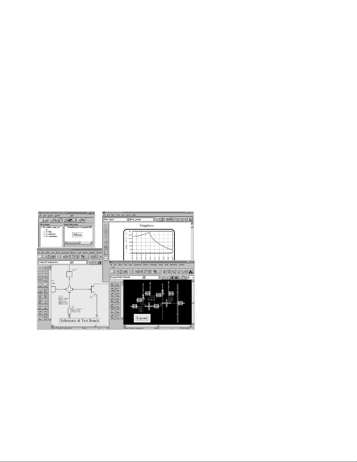
Figure 1. Tools such as Agilent’s Advanced Design System (ADS) provide an intuitive,
windows-based interface. Throughout this document, ADS is utilized to demonstrate
all models, schematics and simulation results. The Main window in ADS, shown at
the upper left, serves as a file manager and a portal to other ADS windows such as
the Layout or Schematic & Test Bench windows. The Graphic Server window (upper
right) offers a visual means of viewing, printing, and analyzing data from completed
simulations.
3
Page 4
Selecting a device
Although an array of process and device technologies
may be suitable for the intended application, the
selected device for this example is an ultra low-noise
amplifier fabricated in a pseudomorphic high-electron
mobility transistor (PHEMT) gallium arsenide (GaAs)
process. The device features 0.5dB NF, +14dBm thirdorder intercept point, and 17.5dB gain at 2GHz, 4V,
60mA. The transistor is optimized for 0.9GHz to 2.5GHz
cellular PCS low-noise amplifiers (LNAs). The wide
gate width of the this device exhibits impedances
that are relatively easy to match, and the 1dB NF
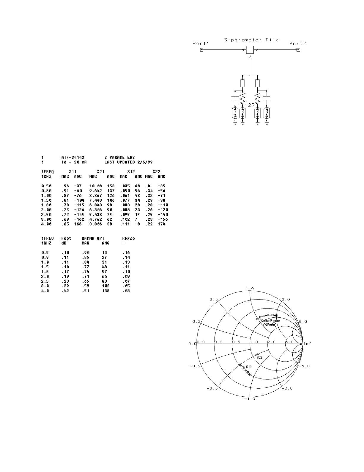
requirement should also be easy to meet. The S-parameters and noise parameters for this device are
shown in Figure 2.
Figure 3. This is the basic schematic of the amplifier using the ultralow-noise ATF-34143 transistor. The model represents the raw device
with source resistance indicated for a self-biased condition.
The model accounts for through-hole vias and selected
source inductances produced by the printed circuit
board. Some source inductance can be beneficial,
because of its impact on input impedance and lowfrequency stability. On the other hand, too much
inductance can cause high-frequency gain peaking,
which results in oscillations. With an 800 micron gate
width, the device in the example design exhibits reasonable tolerance to these effects. However, these
parasitics need to be included in the model since
they affect input and output impedance, which must
be matched.
Figure 2. S-parameters and noise parameters for the ultra-low noise
transistor in the design example (the Agilent ATF-34143). The file, as
shown, is downloadable from the Agilent website formatted for use
directly with ADS.
Raw device modeling
The schematic of the amplifier device, shown in
Figure 3, reveals some source resistance for self bias.
This configuration forces the gate negative with
respect to the source, allowing the drain current to
be set with the source resistor (Rs=Vgs/Id). This
simple biasing technique is very appealing, since it
reduces the overall parts count. The source resistor
is AC bypassed, using a low-impedance capacitor
with the desired operating frequency.
The Smith chart in Figure 4 provides a convenient
way to examine the various impedances for the target device, which in turn can be leveraged to synthesize an appropriate matching network.
Figure 4. Simulated noise and S-parameters for the transistor model,
with S11, S22 and NFmin plotted on a Smith chart.
4
Page 5
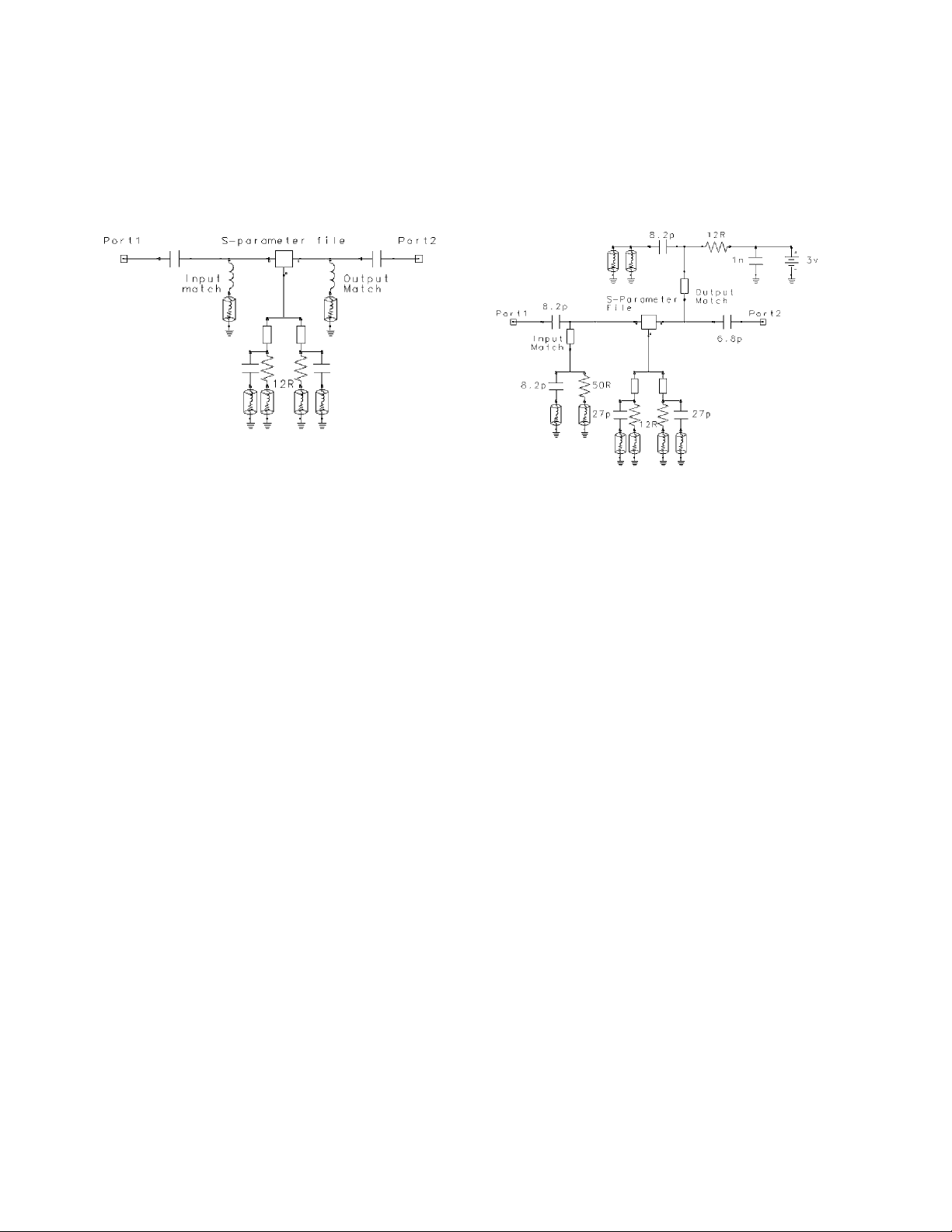
Device matching
Design completion
From the Smith chart it is clear that the device exhibits
some capacitive behavior. Therefore, the matching
network can be a simple high-pass impedance circuit
fashioned from a series capacitor and shunt inductor
as seen in Figure 5.
Figure 5. Since the device is capacitive, a simple high-pass impedance
circuit can be used for the matching network.
The high-pass topology is especially well suited for
personal communications services (PCS) and wireless
LAN applications since it offers sufficient low-frequency
gain reduction, which can minimize the amplifier’s
susceptibility to cellular and pager transmitter overload. A similar high-pass structure is used for the
output impedance matching network, which is optimized for best-return loss and output power.
There are a number of options to determine component
parameters for the matching network. Manual calculation using the device’s impedances represents the
most basic approach. Alternately, while most engineers
are reluctant to use the Smith chart, it provides a
simple, intuitive way of manipulating impedance, and
therefore developing matching networks. Modeling
software is another method of synthesizing and optimizing matching networks based on input and output
impedances.
After the initial optimization, finishing touches can be
made to the amplifier model. Inductors are replaced
with distributed elements and discrete components
are replaced with parts from vendor libraries as seen
in Figure 6.
Figure 6. Here are the synthesized matching circuits for the ultra-lownoise transistor example. After requirements for input and output return
loss, NF and gain are entered, the software optimizes matching circuit
parameters for best results. Inductances are substituted with distributed
elements and discrete components are replaced with behavioral models
of actual parts from vendor libraries.
The 50Ω resistor between the input inductor and
ground provides a DC return for the gate terminal of
the device. This also supplies an effective low-frequency
resistive termination for the device, which is necessary
for stable device operation. In addition to being part
of the matching network, the output inductor
doubles as a way of decoupling the power supply.
With all components defined and the effects of
through-hole vias included in the model, the circuit
is once again optimized and its performance is
assessed. At this point, parameters and components
can be re-tuned if required.
5
Page 6
Design verification
Layout and prototype
Performance simulation
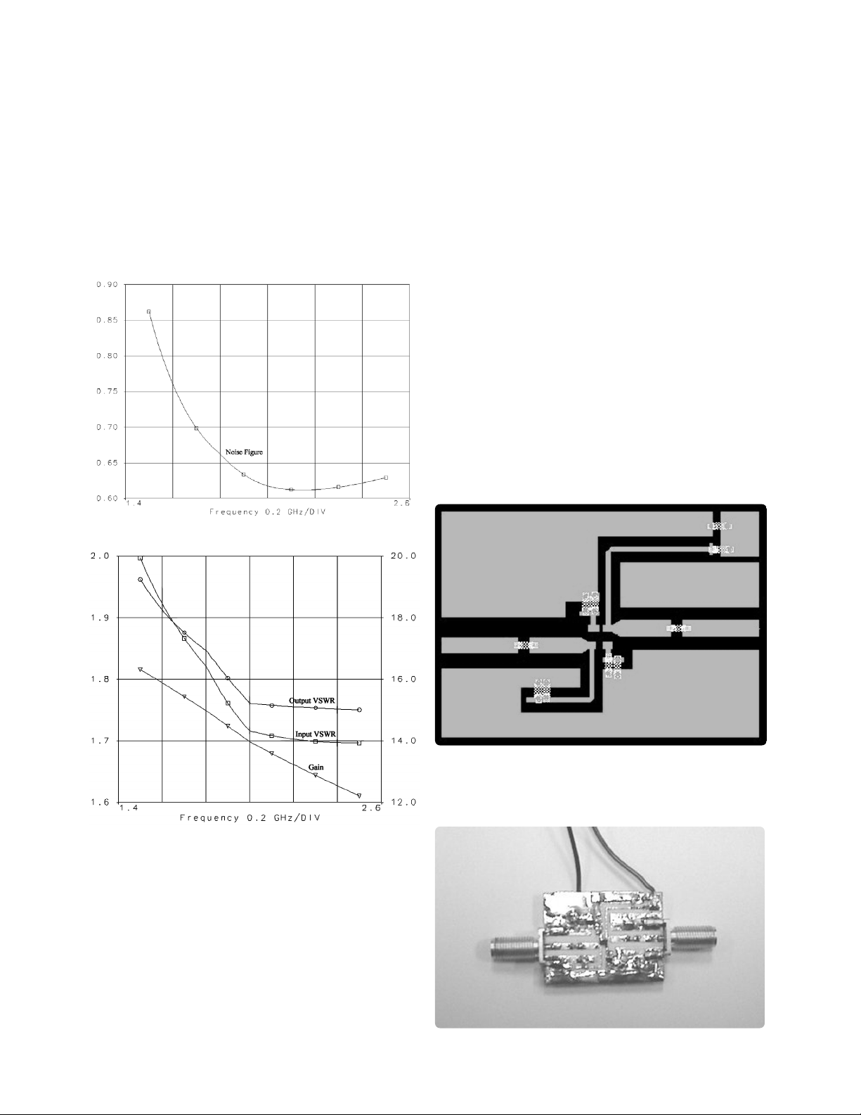
When the finished design is simulated, it looks like
the effort is on track so far. NF for the amplifier easily
meets the requirement of less than 1dB, peaking at
around 0.85dB as seen in Figure 7. The design also
supplies adequate gain. Input and output VSWRs are
also entirely respectable, although they do peak at
the specified upper limit of 2.0:1.
No matter how good simulations look, the ultimate
goal is a working circuit. Simulations are wholly
dependent on the accuracy of device models – they
cannot replace actual measurements on real circuits.
Simulation is merely a tool that speeds up the design
process. The real ‘proof of the pudding’ is in the prototype circuit.
Creating the prototype starts by generating a layout
for the amplifier as shown in Figure 8. Once the schematic is imported into a layout tool, such as the Layout
module in ADS, components, grounding planes, and
transmission lines are placed. The distributed inductors,
which can clearly be seen in Figure 8, were intentionally made longer than required to enable later
modification.
Layouts created in one software modeling tool can
usually be ported to other tools. This simplifies the
task of developing sub-systems of a design independently, for later integration. The layout shown in
Figure 8 was used to build the finished prototype in
Figure 9.
Figure 7. These plots show simulated NF as well as gain and match for
the finished amplifier design.
Figure 8. This layout was generated in a layout tool directly from the
schematic. The layout was printed on high-quality film using a standard
inkjet printer, which was then used to produce the PCB from Rogers
4350 material for the prototype.
Figure 9. The prototype amplifier.
6
Page 7

Design fine-tuning
Performance measurements
Now the initial design work can be verified. In this
example, Agilent’s N8973 Noise Figure Analyzer is
used to measure the performance of the prototype.
First, the analyzer is configured for a 1.5 to 2.5GHz
sweep and calibrated. This is accomplished by
feeding the noise source directly into the instrument.
The analyzer then measures its own noise figure at
various attenuator settings. This is used in the
corrected measurement to remove the effects of the
analyzer.
Once calibration is complete, corrected measurements
for NF, Y-factor, gain, and effective temperatures, can
be executed with the prototype amplifier connected
between the noise source and the instrument. Figure 10
shows the actual screen capture of the NF as measured
and plotted by the analyzer.
Unfortunately, the measured performance falls short
of what was predicted by simulation. The NF peaks
at over 1dB at the band edges. On the other hand,
performance results at the middle of the frequency
range is quite good, at less than 0.7dB. The effects of
nearby mobile phones can also be seen on the plot,
which is to be expected when measuring an unscreened
circuit.
The measurement results don’t tie directly back to
the simulation results, but they do provide a good
starting point for further improvement to the design.
In any case, the design must be modified in order to
meet the required specifications.
A number of parameters can be altered to reach the
desired results, including changing component values
or trace dimensions. The strategy of using distributed
elements may even be suspect, being replaced with a
scheme that uses lumped elements with higher Q
values instead. Once any of these modifications are
made, changes in performance can be monitored
using the analyzer and added to the simulation for
the next design iteration.
Network measurements
Simulation software can also ease the task of gathering
and analyzing data from measurement instruments.
Contemporary simulation tools generally include
some form of general purpose interface to enable the
transfer of data with measurement instruments.
This feature was used to capture the measured Sparameters from a network analyzer for the amplifier example.
The plot in Figure 11 shows the gain and VSWRs of
the example amplifier. The gain easily meets the 10dB
requirement, but the VSWRs are a bit on the high side
at the low frequency end of the band. This is probably
tolerable since the intended frequency bands are 1.8
and 2.3GHz. The required design iteration could very
well improve this situation.
Figure 10. Screen capture of the measured performance of the amplifier
prototype plotted on a noise figure analyzer. The data is corrected for
second-stage effects generated by the analyzer.
Figure 11. Gain and match ported to ADS, and plotted to simplify analysis.
7
Page 8

Narrow band NF measurements
Due to the random nature of noise, noise-power
measurement accuracy improves as bandwidth or
noise exposure time increases, and both parameters
have an averaging effect. In addition, the cumulative
average of many measurements can be calculated to
increase accuracy even further.
Noise-exposure time is a fixed value in NF measurement
equipment. Earlier NF measurement instruments
also had a fixed value of 4MHz for band-width,
while their primary use was for defense applications – in particular, radar. This provided a good
trade-off between measurement time and accuracy
for a given number of averages.
For scores of modern applications, a 4MHz bandwidth
is still acceptable for NF measurements. However, the
explosion in wireless communications and increasing
congestion in the radio spectrum have increased the
need to assess NFs over much narrower bandwidths.
The following example will help illustrate this point.
As shown in the receiver model, the signal enters the
system via an antenna. Generally, the signal is then
passed through an isolation stage to provide a good
match to the amplifier, and possibly split the transmit
and receive paths. Next comes a bandpass filter to
separate the image frequency and remove any adjacent high-power signals.
The critical low-noise amplifier, usually with a NF of
0.5dB or better, follows the bandpass filter stage. The
gain of this amplifier effectively helps to overcome
any NF added by subsequent stages, thereby making
them less critical in terms of NF, but not insignificant.
Why measure narrow band NF?
Figure 13 illustrates the layout of the GSM (global
system for mobile communications) band, the world’s
leading mobile phone service. Transmit and receive
bands are each 25MHz wide, spaced 20MHz apart.
As shown, the receiver input filter must pass the
entire 25MHz band.
Receiver sensitivity
Figure 12 is a simplified representation of a receiver
front-end for a mobile phone or base station application. Good receiver sensitivity is extremely important,
since it enables detection and resolution of weaker
signals. As receiver sensitivity increases, transmitter
power can be reduced, which leads to benefits such as
smaller phones and increased battery life.
Antenna
Low noise
Band
pass
filter
Simplified receiver front-end
Figure 12. Simplified receiver front end for a mobile phone or base
station application.
A direct correlation exists between receiver sensitivity
and NF (i.e., if NF is reduced by 1dB the receiver gains
1dB of sensitivity, or vice versa). With receiver sensitivity representing a key metric for product differentiation between manufacturers and service providers
today, NF has become an extremely important parameter.
amplifier
124, 200 kHz wide channels
Receiver input filter
Example: GSM
Mobile Tx
890 900 910 920 930 940 950 960 970MHz
Figure 13. Example GSM signal arrangement.
Mobile Rx
A GSM base station must accommodate a very sensitive receiver and a high-power transmitter (maybe on
the order of 50dBm) in the same location. The signals
are separated by little more than 20MHz. Plus, there
are likely to be other high-power transmitters for different wireless services at the same location.
In order for the receiver to effectively perform its
function, the input filter must deliver extremely sharp
roll-off characteristics coupled with robust out-of-band
rejection capabilities. Cavity-type filters are generally
employed for these applications.
The 25MHz wide GSM band is split up into 124, 200kHzwide channels. With a cavity-type filter at the receiver
front-end, the filter roll off can potentially impinge on
the channels at the edges of the band. If this happens,
it would cause signal loss in these channels before
the amplifier, resulting in higher NF and rendering
them less effective than mid-band channels. Thus,
system developers must be able to measure NF of
specific channels – not just the overall band.
8
Page 9

Narrow band example
Measuring narrow band NF
Let’s take a look at a narrow-band example. For this
demonstration, a SAW filter is combined with a minicircuits amplifier block as shown in Figure 14. This
arrangement yields an amplifier with approximately
440kHz of bandwidth. The NF of this arrangement is
high, due to approximately 8dB of loss from the SAW
filter, but the example still serves as a good illustration.
In a real-world application, a filter with low loss in
the passband would be used to minimize NF.
Figure 14. The narrow-band amplifier example combines a SAW filter
(~440kHz) with an LNA.
The gain of this filter-amplifier combination measured
on a network analyzer is around 14.5dB as seen in
Figure 15, which serves as a reference. Intuitively, a
plot of NF would roughly be the inverse of the network plot (i.e., the NF is low where the gain is high,
and vice versa). In a real design, this filter-amplifier
combination would be modeled, optimized for lowest
NF, prototyped, measured, and then fine tuned to meet
all specifications for the design.
Figure 16 shows the measurement results of the narrow-band amplifier using the standard 4MHz of noise
bandwidth afforded by older noise figure measurement
instruments. The frequency response shown here is
significantly different from that measured using the
network analyzer. The gain is much lower and the NF
does not have the expected inverse shape.
There are two reasons for this. First, the DUT’s bandwidth is much narrower than the measurement bandwidth, resulting in a linear convolution between the
instrument’s frequency response and the DUT’s
frequency response. The same effect occurs on a
spectrum analyzer if the IF bandwidth is not chosen
correctly, resulting in a plot of the IF filter response
rather than the response of interest.
Figure 15. Checking the response of the narrow-band example circuit
on a network analyzer reveals about 14.5dB of gain over 440kHz of
bandwidth.
Figure 16. Narrow-band amplifier gain and NF measurements using the
customary 4MHz noise bandwidth.
The second reason for the measurement difference
is that the band-pass filter does not shape the noise
floor of the amplifier the same way that it shapes the
signal level or, in the case of a noise-figure measurement, the hot noise power from the noise source.
Although the noise power entering the instrument is
in a narrow band, since the instrument observes this
power over 4MHz, it calculates a lower dBm/Hz
value. This results in a NF plot with the wrong shape
and an artificially high value.
9
Page 10

The plot in Figure 17 shows the same measurement
using a narrower 100kHz bandwidth – more than four
times less than the DUT’s bandwidth. Here, frequency
response is closely correlated with the previous network measurement. Also, NF is much lower and
exhibits the expected shape.
Figure 17. Narrow-band amplifier gain and NF measurements using a
100kHz noise bandwidth.
With older NF analysis equipment, true results are very
difficult to achieve, and the resulting uncertainties
make them unrealistic for measuring modern devices.
The Agilent N8973 NFA makes the measurement easy,
however, as with all noise measurements, there is a
time penalty that must be paid for making accurate
narrow bandwidth measurements.
Microwave NF measurements
Modern measurement instruments easily handle frequencies up to 3GHz. Above that, signals can still be
measured with the aid of an external mixer, local
oscillator, and filters. The mixer can down-convert a
microwave signal to a frequency that can be handled
by the analyzer. If the analyzer has a second interface
port, it can be used to control the frequency and
power level of a signal generator, which serves as
the LO (local oscillator).
Microwave measurements are a bit more difficult.
Systems can employ single-sideband (SSB) or doublesideband (DSB) measurements. It is also important
to make sure that the LO frequency does not appear
in the pass band of the instrument, since high LO
leakage power (relative to noise) from the mixer is
likely to cause the analyzer to range incorrectly. When
choosing an LO, it is important to choose one that
exhibits low phase noise. Otherwise, filters will be
required to ensure that the phase noise is not added
to the overall system noise figure.
Swept LO
In the setup illustrated in Figure 18, the LO is configured to sweep synchronous with the input frequency,
and the analyzer is set to a fixed IF frequency. After
the IF frequency and range are set, the analyzer calculates the frequencies for the LO sweep.
Figure 18. After setting IF frequency and input frequency range, the instrument calculates the LO frequency. Then the instrument is calibrated by
connecting the noise source directly to the mixer. After calibration, the
DUT is inserted between the noise source and the mixer, and corrected
NF and gain are displayed.
10
Page 11

Calibration is accomplished in the same way as an RF
calibration. The noise source is connected directly to
the RF input of the mixer and a user calibration is
performed to measure the NF of the entire system,
including the mixer, cables, and adapters. The DUT
is then placed between the noise source and the mixer
and a corrected measurement is made.
DSB measurements are achieved by taking the average of two measurements spaced at twice the IF frequency. A relatively low IF frequency is desirable to
keep the measurements close together and minimize
the effect of averaging, which increases measurement
uncertainty based on how rapidly gain or NF varies
with frequency.
There is no need to correct for different power levels
of SSB versus DSB measurements, since the total
measurement bandwidth is the same for calibration
and measurement. The analyzer will display the correct gain and NF values.
SSB measurements can also be carried out with the
LO sweep setup, perhaps to remove the effects of
averaging. In this case, an appropriate low-pass filter
is required between the DUT and the mixer to remove
the upper sideband signal, as seen in Figure 19.
Swept IF
It is not necessary to perform measurements using a
swept LO. With some instruments, the LO can be a
fixed value and the instrument’s input frequency can
then be set to sweep in synch with the input frequency. Once the LO frequency and RF input frequency
range are set, the analyzer calculates the frequencies
for the IF (instrument) sweep.
Swept IF measurements are only appropriate for SSB
measurements, which requires the low-pass filter
seen in Figure 19. For example, consider a measurement between 3.7 and 4.2GHz with LO fixed at 3.95GHz.
A DSB measurement would yield the same results
for the average of the two side bands (LO±IF),
regardless of the IF value.
Calibration of the swept IF setup is the same as
swept LO with the exception of the low-pass filter,
which must be in place for both calibration and
measurement.
Figure 19. SSB measurements require the use of a low-pass filter
between the DUT and the mixer.
11
Page 12

Mixer and receiver NF measurements
The NF for mixers and receivers can be measured
using the setup in Figure 20. Calibrating this setup
requires an analyzer with a “mixer measurement
mode.” Once the instrument is set to the correct IF,
LO and input frequencies, the noise source is connected directly to the instrument and user calibration
is performed. After calibration, the instrument will
not display 0dB plus jitter even without the DUT
connected, since the instrument uses the microwave
frequency ENR (excess noise ratio), while the input
is tuned to the IF.
When a mixer is connected directly to the analyzer,
actual conditions are measured. That is, if the external
mixer is configured to reject one side band, a SSB
result is displayed. Similarly, if both sidebands are
converted by the mixer, a DSB result is displayed.
Thus, care should be taken when interpreting results,
since confusion can occur if DSB results are used to
predict performance of a SSB system.
Also, when making DSB measurements of mixers,
receivers, or other frequency-converting devices, the
measured gain will be 3dB higher than the equivalent
SSB measurement. This is because the measured
bandwidth is effectively twice the calibrated value.
Similarly, NF will be 3dB low. Some noise figure analyzers may include loss-compensation features that
will correct this error, but the correction is only
accurate if the gain (conversion loss) in each sideband
is equal.
Using a swept IF configuration with the setup in
Figure 20, the NF of a complete receiver can be measured, assuming access is available to the receiver
IF. Both DSB and SSB measurements are possible.
Figure 20. Mixers can be measured using either a swept LO or swept IF.
With receivers, measurements are performed using swept IF, as the LO
is part of the receiver. Both DSB and SSB signals can be measured, but
care must be takent when interpreting results. User calibration is performed with the noise source connected directly to the instrument, and
the instrument calibrates using ENRs (excess noise ratios) at the IF
frequencies. It then uses the ENRs at the RF frequencies during measurement.
12
Page 13

Measurement uncertainty
Extraneous signals
Satellite and mobile communications applications rely
on monolithic and discrete semiconductor devices
with increasingly-diminishing NFs. This also intensifies the pressure on engineers to reduce NF measurement uncertainty. Many factors can affect the uncertainty of NF measurements, including:
• Extraneous signals
• Nonlinearity
• Instrumentation uncertainty
• ENR uncertainty
• Mismatch
• Measurement architecture
• Instrument NF
• Unwanted in-band power
The following equation can be used to estimate overall NF measurement uncertainty.
2
{
[(
[(
[(
[(
(
F
12
F
1
F
12
δ
G
F
1
1
F
–1
2
δ
G
F
1
1
F
12
–
F
F
1
δ
(
(
1
NF
G
F
NF
2
G
[
+
12
2
[
+
2
2
[
+
(dB)
1
2
0.5
{
[
(
δ
ENR
1
Pagers, security communication systems, wireless
phones, and cordless LANs are all common sources
of intermittent and potentially-disruptive signals at
rather high power levels (a good illustration of this
was revealed in the previous amplifier example). Older
computers can also be a problem, while newer designs
provide much better shielding. The points at which
these signals enter the measurement setup are shown
in Figure 21.
Figure 21. Spurious noise can enter the test setup from external devices
or connected components. Choosing a measurement instrument with
good sheilding is critical for NF measurements, since DUTs are often
connected directly to the instrument. Well-designed instruments will
exhibit very low emissions in the near field.
where, F1is the linear noise figure of the DUT, F2is
the linear noise figure of the noise figure instrument,
F12is the linear noise figure of the complete system
(DUT and instrument), G1is the linear gain of the
DUT, and the δ terms are the associated uncertainty
terms in dB.1In the following sections, the various
uncertainty components are explored in more detail.
In some cases these sources must either be removed
or the measurement setup moved to a shielded room.
Shielding techniques should be designed to reduce
extraneous signal levels by 70 to 80dB, particularly
near transmitters.
One source that cannot be removed in a shielded
room is the measurement instrument. If the DUT is
connected directly to an instrument that does not
incorporate adequate internal screening, any spurious
signals emanating from the instrument increase the
uncertainty of the measured results.
For this reason, NF analyzers are typically heavily
screened, beyond what is called for by standard farfield EMC emissions qualifications, which are not
adequate. Instead, these instruments are normally
required to meet much more rigorous near-field emissions specifications.
1
The derivation of the NF measurement uncertainty equation can be seen in Microwaves & RF Magazine, October 1999, available at www.mwrf.com
13
Page 14

Nonlinearities
Instrumentation uncertainty
It is impossible to measure the NF of a nonlinear device.
Noise measurement can only be accomplished when
both the hot and cold powers from the noise source
are constrained to straight lines. If the DUT behavior
is nonlinear, Y-factor is distorted and NF cannot be
accurately measured. Figure 22 shows a plot of a
device with a degree of compression, resulting in a
NF measurement that is too high.
Figure 22. NF measurements appear too high for nonlinear devices.
Elements such as AGC (automatic gain control),
regenerative circuits, and limiters (e.g., frequency- or
phase-locked loops) add nonlinear behavior to equipment that makes noise characterization virtually
impossible. Thus, the NF of sub-systems should be
measured before these elements are added.
The primary component of instrumentation uncertainty is the linearity of the noise power detector. An ideal
power detector response would be along the horizontal axis of the graph in Figure 23, which illustrates the
behavior of a representative noise figure meter.
0.02
Power Detector Range (dB)
-20
Y-Factor
Error
Figure 23. This shows the typical response of the power detector in the
Agilent 8970B Noise Figure Meter, which is intentionally designed so
that hot noise power falls within the top 5dB window of the detector
response. The NF error in a 11dB Y-factor due to nonlinearities is about
30mdB (i.e., NF=ENR-10Log(Y-1)), which is actually quite good. Instruments not optimized for measuring noise, such as spectrum or network
analyzers, typically exhibit much poorer linearity.
-15
-10 -5
P cold
Y-Factor
P hot
0.01
0
-0.01
-0.02
-0.03
Deviation from Ideal Responses (dB)
-0.04
The nonlinear effects of the power detector are present in every calibration and measurement regardless
of the DUT’s characteristics. This effect can be minimized by choosing a noise source with a lower ENR,
which exercises less of the detector’s dynamic range
and yields behavior that is more linear.
Instrumentation uncertainty is a key measure of the
raw performance of NF measurement equipment –
differences between instruments as little as 50mdB
can have a significant effect on overall measurement
uncertainty. This feature should be a primary concern
when choosing equipment.
14
Page 15

Excess noise ratio (ENR) uncertainty
Mismatch uncertainty
The ENR uncertainty of the noise source can be an
especially large component of measurement uncertainty. Any ENR error transfers directly to the NF,
since NF=ENR-10Log(Y-1). Typical ENR uncertainty
specifications for noise sources are currently around
0.1dB. The plot of a representative noise source is
shown in Figure 24.
ENR Uncertainty
16
15.6
15.2
ENR (dB)
14.8
Figure 24. ENR uncertainty in a typical noise source.
Since specifications for ENR uncertainty in noise
sources are currently covered by recommendations
from the National Institute of Standards and Technology (NIST), there is little that an engineer can do
to improve this parameter. At the very least, care
should be taken to ensure that noise sources are routinely calibrated and that the proper calibration tables
are used.
With previous-generation instruments, calibration
tables were entered into the measurement equipment by hand – a process that was both difficult and
prone to error. Modern equipment eliminates this
source of error because calibration table data is
loaded directly from a disk or transferred via a standard interface, which is desirable for production
environments.
Uncertainty Window
Frequency (GHz) 26.5
Noise-power reflections from noise sources and
attached devices produce extremely complex effects.
The VSWR of the noise source represents a potentially large source of error. Low ENR sources (5dB
or less) with higher internal attenuation provide the
best accuracy. This is due to lower VSWR and better
consistency between on and off impedances.
Figure 25. Noise-power reflections can come from external noise
sources as well as attached devices, increasing mismatch uncertainty.
Placing isolators on the links between the DUT, the
noise source, and the instrument can provide relief
from these effects, but the isolators add insertion
loss and hence another uncertainty component. DUTs
with high gain are more immune to the effects of
mismatch uncertainty, since higher gain reduces the
relative contribution of second-stage NF from the
instrument.
Some manufacturers recommend reducing the
effects of mismatch uncertainty through the use of
S-parameters. But S-parameters reveal nothing about
noise performance. If S-parameters are used without
noise parameters they are likely to introduce more
errors than they remove, in addition to adding their
own uncertainties.
15
Page 16

Instrument architecture uncertainty
Unwanted in-band power
The primary ingredient of instrument architecture
uncertainty is the frequency translation that must
occur to allow the equipment to make measurements
at reasonable IF frequencies. The instrument architecture is either SSB or DSB.
The DSB architecture is used for network analyzers,
meaning that the power in the unwanted sideband is
subsequently measured by the detector. This power
cannot be isolated and therefore causes measurement
error. This is exactly the same sort of problem
encountered when making microwave measurements
with external mixers. SSB architectures are immune
to this kind of uncertainty because the unwanted
sideband is filtered out of the signal.
Instrument NF
The ratio of system (DUT and measurement instrument)
noise factor (linear) to DUT noise factor is expressed
as F12/F1 in the measurement uncertainty equation.
This ratio can never be smaller than one, but has a
significant effect on overall uncertainty as the value
increases above one.
System NF (10logF12) is a function of the instrument’s
NF, plus the gain and NF of the DUT. Overall measurement uncertainty increases significantly as F12
increases. This problem may be most apparent when
using external mixers. In this case, uncertainty can
be improved by inserting a low-noise amplifier before
the mixer during calibration and measurement. High
gain DUTs also reduce F12, but as the DUT gain
increases, the NF of the instrument also increases
due to RF ranging.
NF analyzers typically include a broadband power
detector that monitors the total power entering the
instrument. This enables the equipment to select the
optimum RF range and maintain linearity. The noise
powers entering the instrument are usually very
small–on the order of -40dBm. High levels of unwanted in-band power will cause the analyzer to apply
attenuators and select a poor range for measurement.
This can also occur if any device in the system is
oscillating due to instability. This effect increases
instrument NF and adds to overall measurement
uncertainty.
LO Feedthrough
Instability, etc.
Gain
Device Response
Frequency
Figure 26. High levels of unwanted in-band power will cause the
analyzer to select a poor range for the measurement, resulting in a high
value for instrument noise figure. This can be avoided by keeping the LO
well out of the band of the instrument and ensuring that devices are
stable and free of oscillations.
Another situation can arise when measuring modern
low-noise devices below their optimum operating
frequencies. For example, a GaAs amplifier only
begins to perform well above a few 100MHz. Below
this point, the NF performance is very poor and gain
can peak to rather high levels. This, in turn, increases the power presented to the analyzer, which can
result in a less than optimal measurement. Since
this kind of amplifier would never be used below a
few 100MHz, the frequency response at the low end
should be limited, possibly by choosing low value
coupling capacitors.
GaAs Amplfier Response
Low Frequency Peaking
Useful Portion
Gain
Frequency
Figure 27. Unwanted amplifier response should be filtered.
16
Page 17

Overall uncertainty
As pointed out previously, many components make
up measurement uncertainty, and each contributes
differently to overall uncertainty depending on specific measurement conditions. Looking at each isolated component provides little value. Rather, the
real value is to calculate an aggregate estimate of
overall uncertainty, while simultaneously identifying
the dominant components to facilitate making
improvements.
The previously-discussed measurement uncertainty
equation was developed by applying differential
calculus to the corrected NF equation F1=F12-(F2-1/G1).
This uncertainty equation is available as a web-based
calculator for practical use as seen in Figure 28 and
Figure 29.2This tool enables engineers to quickly
assess NF, NF measurement uncertainty, and identify the components that have the biggest effect on
overall uncertainty.
The calculator enables various parameters to be swept
between two limits, and provides a graphical representation of how overall uncertainty will vary with
any chosen component.
Figure 28. This is the web-based noise-figure measurement uncertainty
calculator data entry window.
2
This web-based NF calculator is available at www.agilent.com/find/nfu
Figure 29. Shown are samples of the results windows for the web-based
noise-figure measurement uncertainty calculator.
17
Page 18

–NOTES–
18
Page 19

–NOTES–
19
Page 20

For more assistance with your test and
measurement needs go to
www.agilent.com/find/assist
Or contact the test and measurement experts
at Agilent Technologies
(During regular or local business hours)
United States:
(tel) 1 800 452 4844
Canada:
(tel) 1 877 894 4414
(fax) (905) 206 4120
Europe:
(tel) (31 20) 547 2000
Japan:
(tel) (81) 426 56 7832
(fax) (81) 426 56 7840
Latin America:
(tel) (305) 267 4245
(fax) (305) 267 4286
Australia:
(tel) 1 800 629 485
(fax) (61 3) 9272 0749
New Zealand:
(tel) 0 800 738 378
(fax) 64 4 495 8950
Asia Pacific:
(tel) (852) 3197 7777
(fax) (852) 2506 9284
Product specifications and descriptions
in this document subject to change
without notice.
Copyright © 2000 Agilent Technologies
Printed in USA 09/00
5980-1916E
20
 Loading...