

Page 1

Series 9800 Desktop Computers
HP 98034
Installation and Service
FliDW
a!~
HEWLETT
PACKARD
Page 2

r/i~
~t:.
HEWLETT
PACKARD
Warranty Statement
Hewlett-Packard
materials
Computer Division
warranty
Hewlett-Packard will ,
which proves to be defective during the warranty period. This
warranty includes labor , parts, and surface travel costs, if any.
Equipment returned to Hewlett-Packard for repair must be
shipped freight prepaid. Repairs necessitated by misuse
equipment, or by hardware, software, or interfacing not provided
by Hewlett-Packard are not covered by this warranty.
NO OTHER WARRANTY
INCLUDING,
OF MERCHANTABILITY
PURPOSE.
CONSEQUENTIAL DAMAGES
For other countries, contact your local Sales and Service Office
•
to determine warranty terms.
applies for ninety (90) days from date of delivery.·
products
and
workmanship
products
BUT NOT LIMITED TO,
HEWLETI-PACKARD SHALL NOT
are warranted against
. For
Hewlett-Packard
sold
in
the U.S.A. and Canada, this
at
its option, repair or replace equipment
IS
EXPRESSED
THE
AND FITNESS
IMPLIED WARRANTIES
FOR
defects
OR
IMPLIED
A PARTICULAR
BE
LIABLE
in
Desktop
of
the
FOR
,
Page 3

98034 HP-IB
Interface
Installation
Manual Part No. 98034-90001
Microfiche
and
No.
Service
98034-99001
Manual
Hewlett-Packard Desktop Computer Division
3404 East Har mony Road, Fort Collins, Colorado 80525
Copyright
by
Hewle
tt
Packard Company 1976, 1
981
Page 4

ii
Printing History
The manual printing
changes
changed
changes
Feb
when a
new
page will
when extensive technical
ru
ary 1981
...
First Edition. Rep la
date
and part
ed ition is printed,
be
indicated
by a revision date at the bottom. The manual part
number
changes
ces
indicate its current edition. The printing
incorporating all
cha nges since the last edition. Each
are made.
the 98 034A HP-IB Interface Manual, 98034-90000 .
date
number
NOTICE
The information contained
HEWLETT-PACKARD MAKES NO WARRANTY OF ANY KIND WITH REGARD TO THIS MATERIAL , INCLUDING, BUT
NOT LIMITED TO, THE IMPLIED WARRANTIES OF MERCHANTABILITY AND FITNESS FOR A PARTICULAR PURPOSE. Hewlett-Packard shall
connection with the furnishing, performance or use of this material.
This document contains proprietary information which
document may be photocopied, reproduced or
Hewlett-Packard Company.
not be liable for errors contained herein or for incidental or consequential damages
in
this document
translated
is
is
subject to change without notice.
protected
to
another program language without the prior written consent of
by
copyright. All rights are reserved. No part of this
in
Page 5

Table
of
Contents
iii
Chapter
Chapter
1:
General
Introduction
98034A
98034B
I/O ROM
Technical
Bus
Functions
Data Transfer Rate
2: Installation
Unpacking
Installation
Interconnecting
Cable
Hardware
Low EMI
Select
Removing the Interface Covers.
Changing
Enabling
Parallel Poll
Code.
Interrupt
System Controller
Information
(Plastic Case) .
(Metal Case)
Cards
and
Length
Cable
Priority
Talk/Listen
Switches
.
Specification
and
Messages ....
......
Inspection
Cables
Restrictions ...........
Con version Kit.
Adapter ........
Addres
Table
..
.
. , . .
.. , ..
, . , . ,
,
of
Contents
. . . . . . . . 1
.
.......
. . . . . . . . . 1
.
........
s.
...
.
.
...
. .... , ,
....
.
, , , . . . ,
. . . . . . .
................
. . . . .... .
...... , ...
..
. . . . . . .
ses
...
...
. . .
...
. .....
. .
........
.
....................... .
..
.......
...
.
. .......... ..
. .
.......
...... ..
.....
.. , .......
...
....
,
...........
. .
..........
. . . . .
........
. . .
...
'. , ...
...
, . .... 8
....
...
...
1
...
2
. .
..
2
.
..
4
6
· , 7
, ... 7
...
8
9
...
9
· . .
9
, 10
.
10
·
. , , 12
, . 13
. . 13
Chapter
3:
Introduction
Functional Test
Replaceable
Calculator
Bus Lines
Data Lines
Control Lines (ATN , IFC, SRQ, EOI ,
Transfer Lines (NRFD,
Data Transfer
Theory of
Select
I/O
Calculator
Calculator
Control
Processor
HP-IB
HP-IB
Service
.. , ....
Assemblies
I/O Lines
and
Operation
Code
Register
Logic
Output
Address
. . ,
.
...
,
Timing.
(D101
Decoder
I/O Data Registers
Interrupt
Interrupt
. . . . . . . . . . . . . . . . . . . . . . . , 19
-
8)
, . ,
...
NDAC ,
....
, . , . , . . . . . . , . .
. .... . , , , , .....
Decoder
. .
Data and Control Bus
and Switch . , ,
and
Logic
Logic
Register.
Calculator
.,
...
. . . . ...........
, ,
......
and
...
. . . .
, . .
...
and
DAV) , . . .
...
..
.......
Command
............ ...
..
, . . . . . . . , ,
...... , ...
Latches.
, . , . , . . . . . . . . .
REN)
..
. . . . . . . . . . . . , . 20
, .
..
, .
....
........
, . , . . . . . . . . .
..
, . ,
..
. . . , .
Register
. .
,
.......
. . . . ..... ..
. ,
. . . .
...........
...
. . .
.....
.........
.
.............
. .
.. , ....
. .... ......
............ , ..
..
...
.. , ..
.....
..
........
....
.
. . .
........
, ... . . ,
. . . . ......
. , .
..
. 15
· . 15
· . 18
..
19
..
. 19
..
19
. . , . . , , 20
, . 22
22
..
23
...
23
24
, .
....
24
..
25
, . , 25
....... , , 25
Page 6

iv
Table
of
Contents
Controlling
98034A
98034B
Replaceable
Circuit
Figures
1 .
2.
3.
4.
5.
6.
7.
8.
9.
10
.
11
.
Data
Input
Multiplexer
HP-IB
Transceivers
Parallel Poll
Initialize
Send
Receive
Read I nterface
Interrupt
Send
Request
Parallel
Interface
Interface
Diagrams
HP-IB
Standard
Low
Opening
HP-IB
98034
Interface
Interrupt
98034
98034
98034A
Logic
Circuit..
the
Interface
Data.
Interface
. . . . . . . . . . . . . .... . .... . . .... . ...........
Data
Operation ...
Service. . .........
Poll.
Parts Lists
Cable
HP-IB
EMI
Cable
the
Three-Wire
Simplified
Status
Status
Detailed
Circuit
Circuit
......
. . .... . . . . . . . . .
.... . . . . . . . . . . . . . . . . . . . . . . . ... . . .... . .
. .
. .
Status . . .... . . . . .....
...
Messages
. . . . . . . . . . . . . . . . . . . . . . .
Assemblies
Assemblies ...... . .... .... . . . . .... . . . . . . . . . .
..
Pinouts .
Cables ... . . .....
Adapter.
Interface
Handshake
Block
Bytes.
Byte.
Block
Diagram
Diagram
.....
..
........
.......................
.....
..
. .... . .... . .
...
.......
. .
....................
....... .....
. . . . . . . . . . . . . . . . . . . . . . . . . . . . . . . .
Case.
Diagram.
. . . . . . . . . . ...
. . . . . . . . . . .
Diagram ......
. . .... .
(Rev . B) . ................
. . . . . . . . . . . . . . . . . .... . . . .
.. ..
. . .
.. ..
. . . . . . . .... . ........ . . . . . . . . . ....
. .... . .
. . . . . ....... . .
. . .
(Timing
...........
. .
...
. . . . . . . .... . . .... .
.
..
......
. . .........
....
...
. . .... . . . ....
. . .
.. ..
......
.. ..
. . .... .
Diagram) ...... .
.
...
. ....... . . . . . . ....
.......
...
. .... . . . . . . .... . . . .
...
. . . ........
. .
.......
. . .
....
...
...
. . . .
..
. .....
. . . .
. . . .
. . .
...
. .
....
.............
. . .... . . . .... .... . .
. . . .
......... . . . .... .
...... . .
....
. . .... . . .... . ........ 33
. .
....
. .
...
...
.
. . . . . . .
...
. .
...
...
.
. .... .
...
...
.
.. ..
. . . . .
..
. . . .
...
........
. . . .
......... . . . .
....
. . . .
. .
...
. . .
......
. . . ....
...... . . . . . .
.
. . .... 26
..
......
..
..
· . 28
.....
. . . . ....
..
..
. . .
· . 32
· . 34
.
...
34-38,41
39,43
...
. . . . 3
...
...
..
...
. .
..
...
. . . .
...
. .
...
.......
....
· . 26
26
26
27
. 28
29
31
32
32
35
. 8
9
11
21
22
30
31
39
43
Tables
1 .
2.
3.
4.
5.
6.
7.
8. 1/0
9.
10.
HP-IB
Signal
98034A
HP-IB
98034
Available
Replaceable
Calculator
Replaceable
98034A
Bus
Messages. . .....
Factory
Bus
Register
Replaceable
Lines ...
Functions
Settings.
Addresses
Assemblies
1/0
Lines
. . . ......... . . . . . . . .... . . .... . . ....... . . . . . .....
Assignments.
Parts ...
......
..............
Parts (Rev. B) . . . . . . . . . . . . . . . . . . . . . . . . . . . .
.. ......
Available
.. ..
. . . . . . . . . . . . . . . . . . . . . . . . . . . . . . . . . .
and
Codes
.....
...
. . . . . . . . . . . . . . . . . . . . . . . . . . . . . . . . . . . . . . . . .
. . . . . . . . . .
.....
........ .....
. .... . ....
.
. . . . ....... . .... . ....
. . . ....
......
...
.........
. . .... .............
.. ..
......
. . . . . . . . . . . .
...
. . . .
...
. . . . .... . . .
. . .
. .
.. ..
.......
...
...
. . .
...
. 3
.....
. 4
. . .... . 5-6
. . . . . .
. . .
.. . .... 41
..
.. ...
..... 18
. . . . .
..
..
..
34-38
12
19
28
7
Page 7

Chapter 1
General
Information
Introduction
The HP98034 HP-I
HP
Interface Bus. The interface conforms to the
top computer to perform a wide variety of operations via
ter, desktop computer and
appropriate
manual
This
description of HP-IB operations
98034A Interface Manual, 98034-90000. All previous versions of the 98034A Interface are
covered here.
98034A (Plastic Case)
The 98034A Interface was revised (rev. E and later) to improve the interface reliability and
interrupt service. This revised version of the
sktop Computers.
both versions of the
B Interface connects
calculator are used interchangeably in this manual, and refer
HP
9800-series computer .
describes
how to install and service the 98034 interface.
is
Replacement parts, component locators, and logic diagrams are shown for
98034A .
given
an
HP
desktop computer (9825, 9835 or 9845) to the
IEEE
Standard 488-1978', allowing the desk-
an HP-
in
the following pages. This manual replaces the
98034A
is
compatible with 9835 and 9845 De-
IB
system. The terms compu-
In
addition , a general
to
an
NOTE
The unrevised version of the 98034A (rev. D and prior) wi
function properly with 9835 and 9845 Desktop Computers.
980348
The 98034B Interface is functionally identical to the 98034A. The metal-case 98034B Interface
provides reduced electromagnetic radiation interference
nent
98034B
, IEEE Slanda
mechanical elements of
(Metal Case)
(EM I). Logic diagrams and compo-
locators are identical to the 98034A rev. E interface. A replacement parts table for the
is
provided.
rd Digital
Interface
for P
Ihe HP-IB syslem
rogrammab
le Inslrumentat ion. This
standard
descr
ll
not
ibes Ihe functional. el
ectrica
l.
and
Page 8

2 General Information
Field
upgrade
connections for the
EMI
is
required. Contact your local
kits are available for desktop computers
98034B Interface. The upgrade kit need only be installed when reduced
HP
Sales and Service office for details.
EMI Upgrade Kits
Low
to
provide the necessary ground
Computer
9825
9835
9845
Upgrade Kit
98273A
98373A
98473A
I/O ROM Cards
The
I/O ROMs
For example , the General
instrument at a time
control of bus functions. After the interface is connected as described
the appropriate I/O
plugged
on
ROM
into the calculator determine which bus operations can be performed.
I/O
ROM
for the
the bus. Use of the Extended I/O
manual for all bus-control operating instructions.
HP
9825A Calculator provides control of one
ROM
, however, enables complete
in
Chapter 2, refer to
Technical Specifications
The bus card's electrical characteristics are listed below. For complete details on HP-IB
electrical , mechanical, and timing requirements, refer to
Select Code
The bus card is preset to select code 7 at the factory. A switch permits changing the setting, if
necessary.
IEEE
Standard 488-1978.
Addresses
The bus card is preset to
pairs of talk/listen addresses can be switch-selected on the card.
Bus
Signal Lines
The bus consists of 16 signal lines as follows:
ASCII talk address "U" and listen address "5".
The pin-outs on a standard HP-IB cable
are shown below .
Anyone
of 30 other
Page 9

General
Information
3
Table 1.
0101
•
HP-IB Signal Lines
Data Input/Output 1
•
• •
•
0108 Data Input/Output 8
DAV
NRFD Not Ready for Data
NDAC Data Not Accepted
IFC
ATN
SRQ
REN
EOI
Data Valid
Interface Clear
Attention
Service Request
Remote Enable
End or Identify
•
SHIELD
.,.
soo
>F
e
NOA
C
NAFO
O.y
.00
0"'"
010'
000.
9'OUndon
,"
I.,
tac.e~'
;TN
SAO
rc
d
NOA
t
NIII'D
OEN
0107
0006
010'
Figure 1. HP-IB Cable Pinouts
Logic Levels
All signals use negative-true logic
(lOW
= logical
1)
•
High >2.
4V
Low <O.4V
+5V
Line Termination
Each of the 16 bus signal lines
Line Drivers
is
terminated as shown
here.
Kn
6.2Kn
t-
Each of the signal lines has a driver circuit with the following characteristics:
Type:
Output Voltage Low State:
Output Voltage High State:
Open Collector
< 0.4 V
>2.4
({t
48 mA
V ({i - 5.2
mA
Line Receivers
Each of the signal lines
is
received with a circuit having the following characteristics:
Hysteresis:
Low State:
High State:
VI
pos. Negative
Positive Threshold voltage 2.0 V
VI
neg . .,.0.4 V
Threshold voltage VI neg.
~V
~0.6
I
pos.
V
Cable Length
A 4-meter cable
is
supplied with the card. Also see "Cable Length Restrictions"
HP
-IB
in
Chapter 2.
Operating Temperature
o - 55° C
Power Requirements
The
calculator supplies all power for the card.
Page 10

4
General
Information
Bus Functions and Messages
The following table lists the HP-IB functions and the capability available with the bus interface.
A
complete description of these interface functions can be found
1978.
Table
2.
Bus Functions Available with the 98034
in
the
IEEE
Standard 488-
Function
SHl
(Source Handshake)
AH
1 (Acceptor Handshake)
T6
(Talker)
L4
(Listener)
SRl (Service Request)
RL¢ (Remote-Local)
PP2
(Parallel Poll)
Implementation
Complete Capability.
Complete Capability.
Basic Talker.
Serial Poll.
Unaddress if my listen address (MLA).
Basic Listener.
Unaddress if my
Complete Capability .
Not Implemented .
Omits capability
talk address (MTA).
of being configured by controller.
DCl
(Device Clear)
DT$1
(Device Trigger)
C1
,2,3,4,5 (Controller)
Complete Capability.
Not Implemented.
System Controller.
Send Interface Clear (IFC
Send Remote Enable (REN).
to
Respond
Send Interface Message.
Receive
Pass Control.
Parallel Poll.
Take Control Synchronously.
Service Request (SRQ).
Control.
).
Page 11

The
interface
generate
certain
automatically
Here
as
details
Message (command or line) Description
calculator
is a
described
.
and
messages
I/O
, as
required
complete
in
previous
calculator
for
controlling
ROMs
, to
list
of
bus
HP-IB
I/O
ROMs
the
. In
many
simplify
messages
manuals.
Table
determine
bus. Some
cases
, the I/O ROM
bus
operation
and
their
Refer to
3.
HP-IB Messages
how
these
functions
functions
for
corresponding
the
are
and
interface
the
user.
appropriate
not
available
bus
I/O ROM
General Information
are
implemented
to
handle
command
manual
the
user
the
functions
or
line
for
5
to
with
name
more
Data
Tr
igger (GET)
Clear
(OCl
or
Remote (REN)
local
(GTl)
local
lockout
SOL)
(LLO)
Transfer instrument-dependent informati
and one or more listeners.
ming informati
Signals a group of selected devices
itiate a set of device-dependent actions .
Causes
power-up state
es
Enabl
ers and device characteristics
messages.
Causes selected instruments
panel)
Prevents local (front or
tions.
on
or data readings.
an
instrument to be initialized
(a
certain range. function, etc.)
remote operation of all devices, allowing paramet-
control.
It may be instrument program-
to
to
be programmed via data
to switch
rea
r panel) control of instrument func-
on
between a talker
simultaneously i
to
a predef ined or
to
local (front or rear
n-
Clear
Lockou t/Local (REN)
Require Service
Status Byte
(SRQ)
(Continued)
Removes
all devices
note.
Indicates a device's need for interacti
Transfers a byte
One bit indicates whether or not the device
ing the require service message. The other 7 bi
indicate device-dependent status.
all devices from Local Lockout mode and causes
to
revert
to
manual contro
(8
bits) of status information
l.
See
on with
is
the controller.
currently send-
the following
to
a listener .
ts
(optional)
Page 12

6
General
Information
Table 3. HP-IB Message (cont.)
Message (command or line)
Status
Bit
Control (TCT)
Pass
Abort (IFC)
When
the 9825 Calculator
automatically outputs
Description
Transfers a
be
may
the controller.
Passes bus controller responsibilities from the current
troller
role.
Halts all
back
pass
single bit of device-dependent status. which
log ically combined with other Status Bit messages to
to a device which can assume the bus supervisory
bus operation and causes control
to the system controller.
to
unconditionally
NOTE
is
the
system controller. pressing 8
the
Abort and Clear Lockout/Local messages.
con-
The
98034 Interface transfers data
second.
talker and listener(s)
The
actual I/O rate can be considerably slower. however. and
on
line at any given time.
actual data rate.
Data Transfer Rate
at
the rate of about
The
45
slowest device always determines the
Kbytes (8-bit characters) per
is
determined by the
Page 13

Chapter 2
Installation
Unpacking
If the shipping carton
unpacked. Inspect the interface for damage. If the interface
electrical specifications, immediately notify the carrier and the nearest
office (offices are
material for the carrier's inspection. The sales. and service office will arrange for the repair or
replacement of your interface without waiting for the claim against the carrier
is
damaged, ask that the carrier's agent be present when the interface
listed
at
the back of this manual). Retain the shipping carton and padding
and
Inspection
is
damaged or fails
HP
sales and service
to
be settled.
to
meet
Installation
Before plugging
system's needs. The switches are preset
A1S1
A1S2
A1S3
A1S3 (6)
A2S1
Switch
(1-5)
in
the bus card, verify that i
Table
4.
Function
Select Code
Parallel Poll Sense
Calculator Address
System Controller
Parallel Poll
Bit
ts
address and function switches are set
at
the factory
98034 Factory Settings
7
Neg-True Logic (position 1)
Talk = U, Listen = 5 (off, on, off, on, off)
Enabled (on)
Bit 1
as
follows:
Factory
Setting
to
your
is
Changing any of the switch settings except select code requires opening the interface case;
see page
After verifying (or changing) the switch settings,
1. Switch the calculator off.
2.
3. Verify that the required I/O
4. Switch the calculator back on.
10
for instructions.
Insert the bus card into
card
firmly into the slot.
see the manual furnished with the
anyone
ROM
install the card
of the I/O slots at the back of the calculator. Press the
is
plugged
ROM
in
to
provide the calculator with bus control;
.
as
follows:
Page 14

8 Installation
Interconnecting Cables
A 4-meter cable
peripheral
the
the new
Length Standard
10.5 meter 10833A
1 meter 10631A 108338
2 meters 106318
4 meters 10631C 10833D
Cabling
device
low-EMI bus cables listed below .
Length
is
supplied with the bus card. The
. Other devices may be
Accessory Number
Low
EMI
10833C
Figure 2. Standard HP-IB Cables
Restrictions
added
piggy-back
to the bus by using either the standard or
connector end is connected to
In
order to ensure
of
length
For
2 m/
devices (10 device x 2 m/
(4 +
than two meters must
connected together using one 4-meter and thirteen 1-meter
Other combinations may be used as long as both requirements are met.
There are no restrictions to the ways
recommended that no more than 3 or 4
device
mechanical
bus
• The total length of cable permitted with one bus card must
meters times the number of
as one device).
• The total length of cable must not exceed 20 meters .
example , there may
device
(8
x 2) = 20). If more than ten
. The resulting structure could exert
proper
cables when they are
= 4 m). Additional devices may
damage
operation of the bus. two rules must
connected
devices
be
up to 4 meters of
device
be
used between some of the devices. For example, 15 devices can be
.
= 20 meters) using one 4-meter and
devices
cables may be connected together . However ,
piggy-back
be
observed regarding the total
together:
be
less than or equal to two
connected together (the interface card
cable
between the first two
be
added
are to be connected together , cables shorter
great
using 2-meter cables
cables
connectors
force on the connector mounting and cause
be
stacked together on one
is
counted
devices
eight
(4
(2
devices x
up
to a total of
2-meter cables
+ (13 x 1) = 17).
10
it
is
Page 15

Hardware Conversion Kit
The
cable supplied wi
M3.9xO.6)
mounting hardware wi
metric hardware is
A convers ion
metric threads. Order
. Earlier bus cables and some HP-IB compatible instruments, however, have
it
th
the 98034 Interface has mounting hardware wi
th
English
black. Do not attempt to mate silver and black hardware.
is available to replace the mounting hardware
HP
part number 5060 -0138.
threads (6-32 UNC). The English
LOW EM I Cable Adapter
The
HP
1 0834A Adapter helps in applications where limited rear-panel space is available for
connecting the new
away from the rear
connector .
low EMI bus cables . The adapter extends the bus cable about 23 mm
panel, prov iding space for other connectors , switches, etc
th
metric threads (ISO
cable
hardware is silver while the
on
any
HP-
IB connector wi
.,
near the HP-IB
I
nstallat
-
th
ion 9
The 1
0834A Adapter
HP
instruments
your
HP
tails.
sales representative for more de-
is
packaged with some
, where
needed. Contact
Figure
Select Code
The select code switch is accessible through a small hole
switch is preset to
small screwdriver.
select code 7 at the factory.
The
Desktop Computer reserves certain select codes (see the Operating and Programming Manual). Those codes are reserved for internal
computer peripherals (display, keyboard, etc). Also do not use
the same code for more than one interface.
To
change the setting, rotate the switch using a
NOTE
3.
The 1 0834A Adapter
on
the top of the interface case. The
Page 16

10
Installation
Interrupt
Some calculator I/O ROMs enable a peripheral -interrupt scheme based
code . Select codes 2 through 7 have a low-interrupt priority, while select codes 8 through
have a high-interrupt priority. If a device on the bus requires fast interrupt service, the interface
should be set to a high-priority select
more
details.
Follow these steps to open the interface case :
1. Switch the
2. Position the interface
shown. Then
screws.
3.
Carefully seperate the halves of the interface case and position them as shown
last photo.
Priority
on
the interface select
code
. See the appropriate I/O
Removing
calculator off; then unplug the interface from both the calculator and the bus.
as
flip the interface over and remove only the
shown
the
Interface Covers
in
the first photo and remove only the four screws
upper
ROM
manual for
-right and lower-left
in
the
15
To
reassemble the interface:
1. Be sure that
other board.
2. Position the
together .
3. Secure the
other screws.
all five pin connectors
cable wires so that they are not crimped as the case halves are pressed
cable-end of the case first, using the two long screws . Then replace the
on
one board are aligned with their sockets
on
the
Page 17

Installation
11
A. Remove only the four screws shown above.
B. Flip the card over and remove the
system
controller
(on)
se
two screws.
C. Separate the case halves and position them
Figure
4.
Opening the Interface Case (98034A shown)
as
parallel poll bit (1)
shown.
Page 18

12
Installation
The
bus interface
be changed
Changing
is
set
to
talk address
to
any talk/listen pair of characters listed
Talk/Listen
"U"
and listen address
through 5) on the A 1 circuit board. Setting each slide
"0" in
the table.
Table
5.
Address
Listen Talk
SP
!
~
II
$
%
Characters
@
A
B
C
0
E
& F
,
(
)
*
+
,
-
/
0 P
1
2
3
4
5
6
7
8 X
9
-
- ,-
i-
G
H
I
J 0
K
L
M
N
0 0
Q
R 1
S
T
U 1
V
W
Y
Z
[
< I
=
>
]
"
-
- i -
i-
Available
Address
(5)
0
0
1
1
1
1 1
1 1
1 1
1 1 1
1 1
1 1 1 1
Bus
Addresses
Switch
(4) (3) (2)
0 0 0
0 0
0 0 0 1
0 0 0 1 1
0
0
0 0 1
0 0 1 1
0 0 1 1 1 7
1
0
1
0
1
0 1
1
0
1 1
1 1 1
1 1
1 0 0
1
0 0 0 1 17
0
1
0 0 1 1 19
0
0
0
0
1 1
SeUings
0 0
1
0
0
0 1
0
1
0
1
0 0
1
1 1
1 1
0 0 0
0 0 1 25
0
0
0 0
1
0
Addresses
"5"
at the factory . These may
in
the next table by setting switch
to
the
"ON"
position corresponds to a
and
Codes
(1
)
0 0 0
1 1
0 2
0
0
1
0
0
0 0
1
0
0
1
1
0 0
1
0
0
1 1
0 0
1
0
1
0
0
1 23
1
0 26
1 1 27
1
0 30
decimal octal
10
11
12
13
14
15 17
16
18
20
i-
21
I-
22
24
28
29
Address
3
4
5
6 6
8 10
9
Codes
0
1
2
3
4
5
7
11
12
13
14
15
16
20
21
22
23
24
25-pr
26
27
30
31
32
33
34
35
36
S3
eset
(1
Page 19

Installation
13
Enablin
Switch S3(6)
system controller function
Switch
poll operation.
using a small screwdriver.
Switch
poll bit.
the "0" position.
S1
S2
on
the A 1 circuit board enables the calculator
on
the A2 circuit board determines which data bit
A2S1
is
preset
on
the A 1 circuit board determines the logic level used when sending the parallel
The
switch
is
preset
g Sy
is
enabled when A 1 S3(6)
Parallel
to
bit 1
to
use negative-true logic.
stem
Poll
at
the factory.
Controller
as
is ON. Refer
Switches
is
output
To
change the setting, rotate the switch
To
use positive-true logic, set A 1
the system controller.
to
the preceding photo.
in
response
to
a parallel
S2
The
to
Page 20

14
Installation
Notes
Page 21

Introduction
Chapter 3
Service
This chapter contains a description of interface operation and instructions
the interface. A
chapter.
Due to the microprocessor-based organization of this interface, it's recommended that the
interface not be repaired to the discrete component
described next, and then the 98034 Test Procedure described
Exerciser.
and
Circuit Diagram to find the defective assembly.
If
you have difficulty repairing the interface or if you would rather have
nearest Sales and Service office for assistance; office locations are listed after the circuit
diagram .
This test checks operation of most 98034 circuits.
follow the 98034 Test Procedure
complete circuit diagram and a list of replaceable parts are at the
level. Instead,
in
your computer's System
If
either test indicates a defective interface, use the following Theory of Operation
Functional
in
your computer's System Exerciser.
Test
To
perform a complete test of the interface,
to
help you repair
back
run
the Functional Test
HP
repair it, contact the
of this
This test assumes that the interface switches are set to their factory settings:
98034 Factory Settings
Switch
A1S1
A1S2
A1S3
(1thru
5)
A1S3 (6)
A2S1
Refer to Chapter 2 for instructions on setting the switches.
Function
Select Code
Parallel Poll Sense
Calculator
System Controller
Parallel Poll
Address
Bit
7
Negative-True Logic (position
Talk = U, Listen = 5 (off, on, off, on, off)
Enabled (on)
Bit 1 (least-significant bit)
Factory
Setting
1)
Page 22

16
Service
To Test the Interface (9825):
1. Plug the interface card into any I/O slot
General I/O
culator.
2. Switch the calculator on and verify the
If the i·
not appear, refer to the 9825 System Test Booklet.
3. When
The first thru fourth status bytes are displayed from left to right, respectively. See page
30 for details
When only a General
ROM
or
an
Extended I/O (with General I/O)
··
· does not appear, remove the interface and press 8 . If the i . display still does
an
Extended I/O
on
status bytes .
ROM
110
is
plugged in, execute this line and verify the display:
ROM
is plugged in, execute this line and verify the display:
on
the back of the calculator. Verify that either a
ROM
is
display.
[,-_! ... _.
___________
plugged
in
the cal-
\J
4. If the display does not return after the line
code switch to 0 and
5. If the display still does not return, or
card
is
defective .
The
numbers returned
Address and/or System Controller switches are incorrectly
back
to
7.
Then repeat the appropriate line above.
if
an
NOTE
in
this procedure
is
executed, press E1 and rotate the select
incorrect number
will
be incorrect
is
returned, the interface
when
the
set
.
Page 23

To Test the Interface (System 35/45):
Service
17
1. Plug the interface into any empty I/O slot on the
ROM
is
plugged into the computer.
2. Switch the computer on and verify that the cursor appears
does not appear on the
refer to your System Exerciser
CRT,
press CONTROL-STOP.
Manual.
back
of the computer. Verify that the I/O
on
the
CRT. If
If
the
cursor still does not
3. Execute the following statements:
~:::;
T
f1
T U
~:::;
? ;
f1
;
E,
C ,
[I
the results are
~
.-
.'
~
i
=_1
The first thru fourth status bytes are displayed from left to right, respectively. See
30 for details
If
the results are not as shown, rotate the select code switch to 0 and back to 7. Repeat
4.
on
status bytes.
step 3.
If
the results still are not
5.
as
shown, refer to the System Exerciser Manual for further
interface verification procedures .
the cursor
appear
page
,
NOTE
The
numbers returned
in
this procedure will be incorrect
Address and/or System Controller switches are incorrectly
when
set.
the
Page 24

18
Service
Replaceable
Assemblies
These assemblies are available for direct replacement:
Table 6. Replaceable Assemblies
Assembly
Calculator 1/0 Logic Board
HP-IB Control Logic Board (A2 or A4)
Cable Assembly:
98034A
98034B
(cable and case-half assembled)
(A
1 or A3)
The 98034A was built with 98034-66501 and 98034-66502 boards
The 980348
is
built with 98034-66503 and 98034-66504 boards
as
HP
as
A3
98034-66503
98034-66504
98034-61601
98034-61611
98034A and 980348 are functionally compatible. However, the A 1 and
be used
and
in
the 980348 .
A4
are interchangeable.
In
the 98034A ONLY: The A 1 and
A3
are interchangeable , and the
Part
Number
A 1 and
and
A2
A2
assemblies.
A4
assemblies. The
assemblies cannot
A2
Page 25

Calculator 1/0 Lines
The
data
and control lines available at the calculator I/O slots are listed on the next
lines are also shown
that negative-true logic is used.
Line
in
the
block
diagram
Table
on page 22. The bar above each line name
7.
Calculator I/O Lines
Signal Direction
(Calc.
Description
<--+
page
indicates
interface)
Service
. The
19
10D~
thru
1007
PAj"thru
~thruiC2
PA3
DOUT
10SB
FLG
STS
!NiT
iR[
11*i
INT
Input/Output Data Lines
Peripheral Address Lines
Register
Direction of Data Transfer
I/O Strobe Line
Interface Flag
Interface Status
Calculator Initialize (reset)
Interrupt Request Low
Interrupt Request High
Demand Response
Code Lines
Bus Lines and Timing
The standard HP-IB signal lines are
by
IEEE
Standard 488-1978.
Data Lines
(0101-8)
(1
= interface ready)
(1
= interface present)
(0-7)
(8-15)
to
Interrupt Poll
described
(1
= output)
next. The function of each line
is
fully
described
The
data
lines are used to communicate all data including input . output and program
addresses
sent one character (byte) at a time (i.e ..
Transfer Lines.
control. and status information between instruments connected to the bus . Data is
byte-serial and bit-parallel) under control of the
In
most instruments .
data
is
based on the 7-bit ASCII code . Unused
terminate in a resistor load.
Control Lines (ATN, IFC, SRO, EOI, and REN)
The five control lines govern the flow
ATN (Attention) is driven
(ATN
is
low) or
data
(ATN
by
the active controller and indicates whether address
is
high) are being transmitted .
of
information over the
data
and transfer lines .
commands
codes
data
.
lines
Page 26

20
Service
IFC
(Interface Clear)
message.
poll mode
no effect
SRO
controller .
EOI
When
the same time that it
REN
operating instruments under remote
use
resistor
When
is
disabled , and control
on
the bus operation.
(Service Request)
SRO
(End or Identify) may be used to indicate the end of
ATN
is
high, the addressed talker may indicate the end of its data by setting
(Remote Enable)
REN
and they monitor
load. The system controller may change the state of
is
used only by the system controller
IFC
is
low for at least 100
is
may be set low
places the last byte
is
it
to
J,Ls
, all talkers and listeners are stopped, the serial
is
returned
driven low by a device
at
any time except when
driven by the system controller and
control. Only instruments capable of remote operation
at all times. Instruments that
to
the system controller. When IFC
to
on
the data lines.
indicate that
IFC
is
an
do
not use
REN
initialize the bus via the Abort
is
high,
it
has
it
wants the attention of the
low.
instrument's character string.
EOIlow
is
one of the conditions for
REN
terminate the line
at any time.
in
at
a
Transfer
The
three transfer (handshake) lines are used
tion
on
technique
tions being placed
complished at the speed of the slowest instrument.
NRFD
data
lines.
NDAC (Not Data Accepted)
by all listeners.
DAV
(Data Valid) indicates the validity of information
information
the
data lines
Data
Lines
the data lines. All instruments use these lines and employ
to
pass information. This allows asynchronous data transfer without timing restric-
(Not Ready for Data) indicates that all listeners are ready to accept information
When
on
(NRFD,
on
any instrument connected to the bus. Transfer of each byte
NRFD
When
the data lines
is
not valid.
is
NDAC
NDAC,
low, one or more listeners are not ready for data .
is
high
to
is
low,
all
is
valid for the listener(s).
and
DAV)
to
execute the-transfer of each byte of informa-
an
interlocked "handshake"
indicate the acceptance of information
listeners have not accepted the information.
on
the data lines. When DAV
When
DAV
is
high, the information
Transfer
on
the data lines
is
low, the
is
on
ac-
the
on
Transfer of data
instruments connected
on
tion
the
on
the bus
data lines are shown
to
the bus.
is
asynchronous. It places
The
timing and levels required
in
the next figure. Transfer
no
restrictions
on
the data rates of
to
transfer a byte of informa-
is
under the control of three
Page 27
Service
21
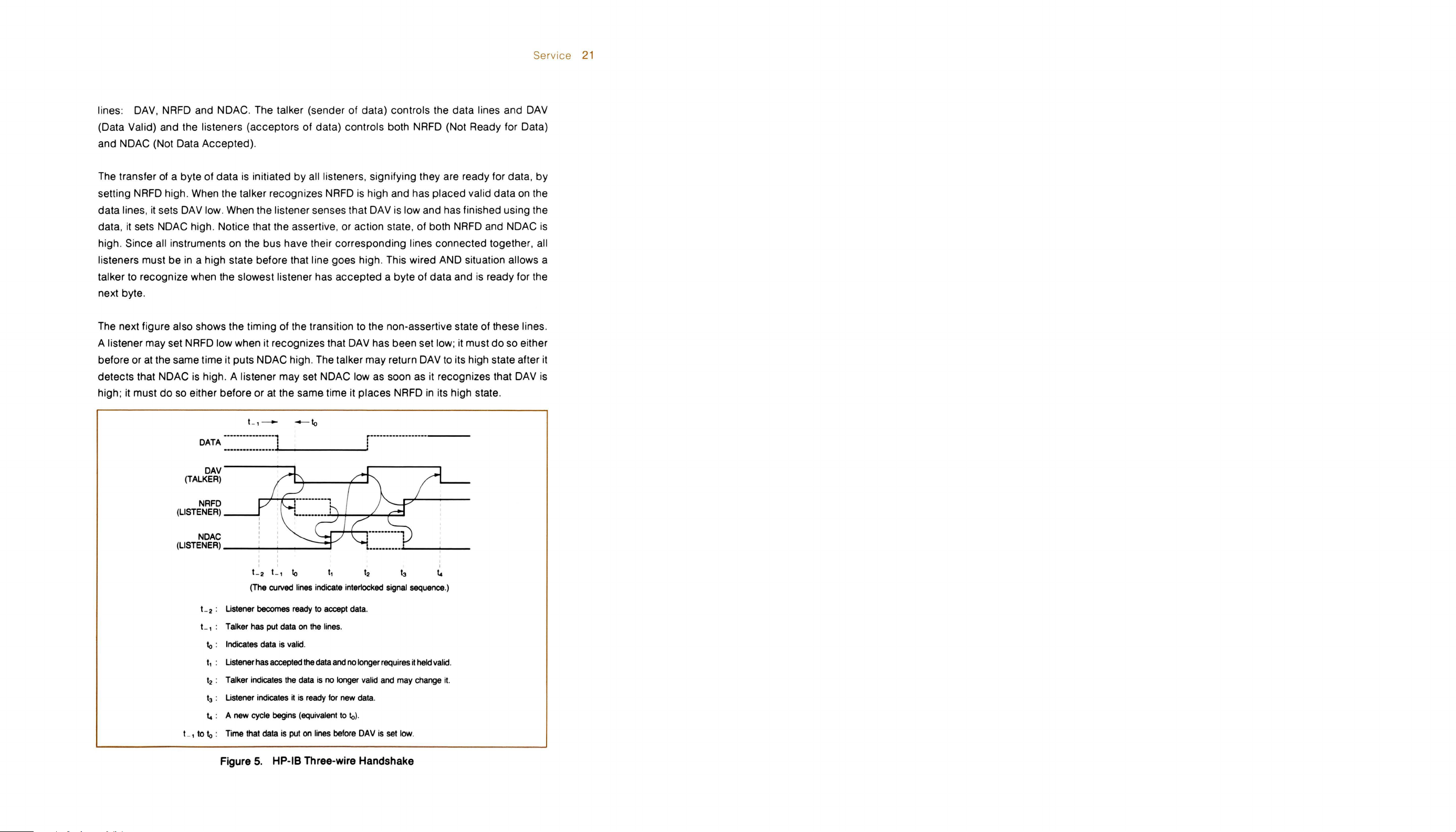
lines:
(Data
and
The transfer
setting
data
data,
high. Since all instruments
listeners
talker
DAV,
NRFD
and NDAC. The talker (sender of data) controls the data lines and DAV
Valid) and the listeners (acceptors of data) controls both NRFD (Not Ready for Data)
NDAC (Not Data Accepted).
of
a byte of data
NRFD
lines,
it
to
high. When the talker recognizes
it
sets
DAV
low. When the listener senses that DAV
sets NDAC high. Notice that the assertive, or action state, of both
must be
in
a high state before that line goes high. This wired AND situation allows a
recognize when the slowest listener has accepted a byte of data and
is
initiated by all listeners, signifying they are ready for data ,
NRFD
is
high and has placed valid data
is
low and has finished using the
NRFD
on
the bus have their corresponding lines connected together, all
is
next byte.
The next figure
also shows the timing of the transition
A listener may set NRFD low when it recognizes that
at
before or
detects that
high; it must do
the same time it puts NDAC high. The talker may return
NDAC
is
high. A listener may set NDAC low as soon
so
either before or at the same time it places NRFD
to
the non-assertive state of these lines.
DAV
has been set low;
DAV
as
it
must
to
its high state after it
it recognizes that DAV
in
its high state.
by
on
the
and NDAC
ready for the
do
so either
is
is
DATA
----------------'1
----------------+.
DAV
(TALKER)
NRFD
(LISTENER)
(LISTENER)
L 1 to
__
NDAC
__
L 2 : Ustener becomes ready to accept data .
Talker has put data on the lines.
L 1 :
10
: Indicates data is valid.
t1
: Ustener has accepted the data and no longer requires it held valid.
t2
: Talker indicates the data is no longer valid and may change
t3
: Ustener indicates
t. : A new cycle begins (equivalent to
10
: Time that data is
-----_
-!
.........
---!I--
__
L2
L1
10
(The curved lines indicate interlocked signal sequence.)
it
is
ready for new data.
put
on lines before
---'
:---------------------
.....
:
t1
it.
10)
.
DAV
is set low.
Figure
5.
HP-IB Three-wire Handshake
Page 28

22
Service
Control Lines
IC1
.IC2
DOUT
Figure
6.
Calculator 1/0
"'"
I
I
I
..
..
Calculator
1/0
Registers
I
I
....
"'"
I
I
I Interface
!
I
I
I
I
I
I
..
...
..
•
..
Calculator
Interrupt
Logic
t
Calculator -
Command
Reg
ister
I
98034 Simplified Block Diagram
Processor Data Bus '"\
..
"'"
Select
..
Code
Switch
CFLG
Bus
Address
Switch
-
•
Processor
and
ROM
..
...
Data Output
Latch
Data Input
Multiplexer
Control
and
Interrupt
Logic
...
"'"
...
.....
"'"
..
..
Bus
Transceivers
Bus
Transceivers
....
HP· B
..
Data:
0101 -
Transfe
DAV
NRFD
NDAC
Control:
IFC
ATN
SRQ
REN
EOI
0108
r:
Theory
The 98034 interfaces the calculator to the HP-IB by performing four major functions: interpret -
control bytes from the calculator , transferring data bytes from the calculator to the HP-IB,
ing
transferring data bytes from the HP-IB
calculator .
the
A simplified block diagram of the interface is shown
interconnections between processor,
the processor,
The processor monitors the status of both the calculator 1/0 and the HP-IB. It determines if the
calculator
the
calculator command register. If this signal
instructions
processor monitors the status of the
SRO, REN
Multiplexer. If
message) the processor issues the appropriate instructions to
quested.
Please refer
section.
Select
The function of the Select Code Decoder
the
calculator. The interface responds only when the code
PA,0
through PA3, matches the select code set
code
enables the interface
is
ready for
the
flag line (FLG) low and setting the status line (STS) low when no error conditions exist on
the interface.
calculator 1/0 and HP-IB.
is
requesting
to
the other modules to
, IFC and EOI) and its transfer lines (DAV, NRFD and NDAC) via the Data Input
a condition is detected that requires action (for example, a Require Service
to
the Complete Block Diagram
Code
Decoder
an
1/0 operation, the interface indicates its presence
an
1/0 operation by monitoring the CFLG (Calculator Flag) line from
and
to
look for
of
Operation
to
the calculator, and transferring status information to
on
the left. The diagram shows the
ROM
, 1/0 registers and other circuits needed to support
is
true, the processor issues the appropriate
decode
HP-IB
and execute the requested 1/0 operation. The
by
periodically sampling its control lines (ATN,
complete the operation re-
on
page 33 while reading the remainder of this
Switch
is
to determine when the interface
on
the peripheral address lines,
on
the select code switch. Receiving the preset
an
1/0 command from the calculator. When the interface
to
the calculator
is
addressed by
by
setting
..
Foldout
Page 29

I/O
Register
Decoder
and
Calculator
Command
Register
Service
23
The I/O Register Decoder
requested by the
looking at the DOUT line. For
by
data
lines
(IOD~
I/O strobe pulse (IOS8) occurs. For
an
interrupt poll (INT), the data
culator
latched into the Calculator Command Register when the I/O strobe pulse (IOS8) occurs.
The Calculator Command Register consists of a 4-bit latch and four open-collector NAND
gates. The
the direction of the
set when the calculator requests
NAND gates and becomes the
flag line (FLG) to go high, indicating that the interface
used to gate the
Read Calculator Command Register (RCCR) instruction.
the requested
Command Register (CCCR) instruction, which clears the Calculator Command Register and
readies the interface for another
data lines. For both input and output, the code
calculator. It determines whether
through 1007)
latch holds the I/O register code
I/O transfer determined by DOUT.
DOUT,
I/O operation and
is
a network of gates which interprets the type of I/O operation being
the
transfer
an
output operation,
is
latched into the Calculator Output Data Register when the
an
input operation when the calculator
in
the Calculator Input Data Register
(R4
an
I/O operation. This bit
Calculator Flag line (CFLG). Setting this line true causes the
IC1
and IC2 signals onto the processor's data bus when
is
ready for another I/O operation,
I/O operation.
the
through
In
is
addition, one bit of
busy.
is
an
data
on
on
the DOUT,
R7)
determined by
is
buffered through one of the
The
other three NAND gates are
When
the processor has executed
it
input or output operation
the calculator input/output
is
not conducting
is
placed
IC1
the
issues a Clear Calculator
on
the cal-
and IC2 lines
IC1
and IC2 and
latch
is
it
issues a
is
always
Calculator
The Calculator Output Data Register consists of two 4-bit latches and eight open-collector
NAND gates . As described earlier, this register holds the data to be transferred from the
calculator to the interface . The data contained
bus when the processor issues a Read
Calculator Input Data Register consists of two 4-bit latches and eight open-collector
The
NAND gates. The data
processor issues the Send Calculator Input Data (SCID) command. The data
transferred to the calculator input/output data lines when the calculator requests
operation.
I/O
Data
Registers
in
the latches is gated onto the processor data
Calculator Output Data (RCOD) instruction.
on
the processor data bus is latched into the two 4-bit latches when the
in
this register
an
is
input
Page 30

24
Service
Calculator
The
Calculator Interrupt Logic allows the interface
several conditions which are described later in the section "Controlling the Interface". The
Calculator Interrupt Logic
the appropriate interrupt request line (IRL or IRH) low when the processor issues a Calculator
Interrupt
(INT). IRL
IRH
is
pulled low when the switch
service request,
poll
is
conducted when INT
(PA3) matches the most-significant address bit from the Select Code switch, the Calculator
Interrupt
switch determines which line
Code
Interrupt
Request (CIRQ) instruction and the calculator
is
pulled low when the select code switch
it
conducts
Logic pulls one of the calculator input/output data lines low. The setting of the Select
Logic
to
request service from the calculator for
is
a network of gates and a one-of-eight
is
not conducting
is
set to
an
is
set between a and 15. When the calculator senses a
an
interrupt poll to determine which interface requires service. A
is
low. When the most-significant bit of the peripheral address
is
pulled low, as shown in the following table:
Interrupt
Select Code Line Pulled
o or 8
1 or 9 1001
2 or 10
3 or
11
4 or 12
5 or 13
6 or 14
7 or 15
Request Bits
Low
100~
1002
1003
1004
1005
1006
1007
decoder
address between 0 and
. This logic pulls
an
interrupt poll
7,
and
Control
The Processor,
interface. The
control lines, the a-bit processor data bus, and selecting I/O registers via the I/O Register
Selector. The algorithms for interface control and the implementation of the HP-IB interface
functions are contained
asymmetrical waveform which
signal
The Processor also contains a vectored interrupt structure for conditions that require immediate action. These conditions are described next.
Logic
ROM
I/O Register Selector, and Oscillator form the control logic portion of this
Processor controls all interface operations
in
the 4096-bit ROM. The Oscillator generates a 2 mHz (approx.)
is
used as the main clock for the Processor and as the enable
for the I/O Register Selector.
by
issuing instructions via seven
Page 31

Service
25
Processor
The Processor I nterrupt Logic
processor for either of two conditions:
• When
• When the control line A
An
interrupt occurs for the second condition only when the calculator
ler .
The processor enables the interrupt logic via the Interrupt Enable (lENA) line.
message is received via the
pulse
on
The
IFC
line was previously set true
When the interface
logic via the Interrupt Enable line, but also sets the Immediate Control line (IMD) true.
Abort message
which initializes all of the HP-IB interface functions.
of the
the DAV line, the NRFD line, and the
the algorithm which controls the acceptance and analysis of the data sent by the controller.
HP-IB sets the
Data Latch and disables the HP-IB Transceivers for the HP-IB data lines (0101 through 0108),
interface ready to receive data from the
the
an
IFC
Interrupt
Abort message (IFC)
line and then initializes all of the HP-IB interface funct ions within the interface.
is
is
received, the interrupt logic generates a vectored interrupt
Logic
is
a network of gates that provides the ability
is
received from the HP-IB or
TN
is
set true by the controller
HP-IB, the interrupt causes the processor to generate a 100
as
the result of
not the active controller, the processor not only enables the interrupt
ATN
line true, the interrupt logic immediately clears the HP-IB Output
EOI
line; then the NDAC line
controller. A vectored interrupt
an
In
in
charge.
is
not the active control-
1/0 operation from the calculator.
addition, when the controller
is
set low. This leaves the
to
interrupt the
When
to
the algorithm
in
is
also generated
an
Abort
When
charge
JJ.s
an
to
HP-IB
The HP-IB Output Data Latch consists of two 4-bit latches. Data
processor data bus into this 8-bit
(SIBD) command. The outputs of this latch are routed to the HP-IB data lines via the drivers
contained in the
The
HP-IB control lines
from the processor data bus into this
Control (SIBC) command. This latch consists of one 4-bit latch and one 0 flip-flop.
of this
HP-IB
The HP-IB Address Register consists of a hex, tri-state buffer and six switches . Five of the
switches are used to set the five least-significant bits of the
each switch
Output
HP-IB
Control Bus Latch
latch are routed
Address
is
off , its corresponding bit
Data
HP-IB Tranceivers.
(EOI
and
Control
latch when the processor issues the Send Interface Bus Data
is
a 5-bit latch which holds the bit pattern to be applied to the
, ATN,
to
SRO, REN
the bus drivers contained
Register
Bus
Latches
is
transferred from the
and IFC). The appropriate bit pattern
latch when the processor issues the Send Interface Bus
in
the HP-IB Transceivers .
HP-IB talkllisten address. When
is
set
to
a logical 1. The HP-IB address switches are
is
transferred
The
outputs
Page 32

26
Service
connected to the five least-significant bits of the processor data bus
addition to the HP-IB address switches, this module also contains the System Controller
switch. When this switch
is
connected
processor data bus when the processor issues a Read Interface Bus Address (RIBA) instruction.
Data
The
function
a
control byte (EOI,
to
the processor data bus.
Bus Data (RIBO) command. The control byte is selected when the processor issues the Read
Interface Bus Control (RIBC) command.
This
module consists of one AND gate and two, quad 2-to-1 multiplexers.
HP-IB
The
interface uses four bus transceiver modules . Two are used for the HP-IB data lines (0101
through 0108) and two are used for the HP-IB control lines (EOI, ATN,
NRFO
and NOOC). These transceivers allow bidirectional flow
between the interface and the
and four receivers with hystereSiS.
to
bit
Input
Multiplexer
of
the Data Input Multiplexer
Transceivers
is on, the interface assumes the role of system controller. This switch
05
of
the
processor data bus. The contents of this register
is
to route either a data byte (0101 through 0108) or
ATN, SRO,
REN,
IFC,
OAV,
NRFO
and NOAC) from the HP-IB Transceivers
The
processor selects the data byte by issuing the Read Interface
of
data and control information
HP-IB. Each transceiver provides four open-collector drivers
(DO
through 04). In
is
gated onto the
SRO,
REN,
IFC,
OAV,
Parallel
The
Parallel Poll Logic provides the capability
controller in charge of the HP-IB.
true) and the calculator has requested service from the controller via the
poll logic
This logic consists of a 3-input NAND gate, a slide switch to set the logic level of the bit, and a
switch to
parallel poll.
Initialize
The
Initialize Circuit applies
This condition
processor to execute
algorithm issues the Abort message (IFC) and sets the
system controller, this algorithm clears all HP-IB interface functions . This circuit also provides
a reset
Poll
Logic
sends one bit of status
select which bit
Circuit
is
indicated by the initialize signal (INIT) from the calculator, and causes the
an
pulse
to
the HP-IB Control Bus Latch.
to
respond to a parallel poll conducted by the
When
the controller initiates a parallel poll
SRO
to
the controller via one data line (0101 through 0108).
on
the HP-IB data lines will be used to send the response to the
+9 V to
initialize algorithm. If the interface is the system controller, this
the processor after all other power supplies are stable.
REN
line true. If the interface
(ATN
and
EOI
line, the parallel
is
not the
Page 33

Service
27
Controlling
The calculator controls the interface via four 1/0 registers,
memory
four registers are not dedicated components
through the
in
registers transfers the data to the interface
load operation from any of these registers into the calculator transfers the data from the
selected interface to the calculator .
The calculator 1/0 signals
below :
locations used for the storage of input and output data.
Calculator 1/0 Registers (see block diagram
the processor's readlwrite memory. A store operation from the calculator to anyone of these
IC1
and IC2 determine which 1/0 register
IC2
0 0
0
the
previously selected by the peripheral address. A
IC1
0
Interface
R4
through R7. These registers are
It
should be noted that these
on
the bus interface. Instead, all data passes
on
page 22) and
Register
R7
R6
R5
R4
is
temporarily stored
is
addressed,
as
shown
The contents of each 1/0 register are assigned unique roles such
(see the next table) . These assignments are described
in
the following pages.
NOTE
The calculator's store and load instructions mentioned here
nal routines, used by
statements and functions. Registers
to
be directly accessible via user-language operations.
1/0
ROM
to
implement
R4
the
through
user-language 1/0
R7
are
as
data, status or control
are
inter-
not
intended
Page 34

28
Service
Table 8.
1/0
Register
Assignments
Send
Data
Register Direction
IN
R4
R5
R6
R7
f
t
OUT Send Data to Bus
IN
{
OUT
IN
{
OUT
IN
{
OUT
1/0 Instruction
Request Data from Bus
Interface Status Request
Interrupt
Null Operation
Send Multiline Interface
Gel Parallel Poll Byte
Send Uniline Interface
Byte
Message
Message
The
least-significant eight bits of data contained
the HP-IB data bus (0101 through 0108) when a Store
transfer occurs only if the interface has previously been addressed
the interface has not been addressed to talk, the calculator status line
Receive
When
places
listen, however, the calculator status line
The
first Load
tially a request data byte instruction. The data byte placed in the Calculator Input Data
Register may be transferred into the least-significant eight bits of the calculator accumulator
by executing either a Load
Load
R6
causes the interface
instructions
byte; the first Load
calculator.
Data
a Load
R6
R4
instruction
it
in
the Calculator Input Data Register. If the interface has not been addressed to
R4
instruction received by the interface after any other
and Load
to
R4
rapidly input data.
R4
is
executed, the interface accepts a data byte from the HP-IB and
(STS)
R6
instruction or another Load
instructions are treated
to
remain
requests the byte and the second Load
in
the input-data routine, permitting successive Load
Two
Load
in
the calculator accumulator
R4
instruction
as
a talker
(STS)
is
cleared and data
R4
instruction.
as
"no operations" by the interface . The Load
R4
instructions are needed to input each data
is
not accepted.
1/0
R4
transfers the byte
is
transferred
is
executed. Data
on
the HP-IB. If
is
cleared.
instruction
In
this case, both the
is
essen-
R4
to
the
to
Page 35

Service
29
Read I nterface
The
calculator
tions . The
calculator
to the
The execution
calculator. The fifth
determined
used to identify the
algorithm,
cessive Load
instruction.
can read the status of this interface
following
:
of
the
by
the
contents
which
transfers
R6
instructions.
Status
by
executing a
table
shows the
Instruction Data Byte
Load
RS
Load
R6
Load
R6
Load
R6
R6
Load
Load
RS
and
sixth bits are always set to a logical 1. The remaining six bits are
of
interface
. This instruction also
each
If
sequence
98034
instruction causes the interface to transfer a
the Calculator
the status line (STS) is clear, it will
Read
HP-IB Interface Signature
First Status Byte (Device Clear and Error)
Second Status Byte (HP-IB Address)
Third Status Byte (HP-IB Control Byte)
Fourth Status Byte (Interface Status)
of
the four additional status bytes to the calculator with suc-
of
instructions and the information transferred
Status
Input
Sequence
Data Register and are ignored . This byte is
causes
the interface to enter a read status
sequence
be
set
of five instruc-
data
by
the fourth Load
byte to the
R6
calculator
The
whenever the interface
has been transferred to the
pleted, however,
message
bytes are summarized on the next
does
in
(IFC), sent
not have to read all four status bytes. The read status algorithm terminates
detects
less than 100 ms. This restriction is necessary to insure that the Abort
by
the controlier in charge, is not missed. The bit assignments of the four
an instruction other than Load
calculator. The read interface status instruction must
page
R6
before the fourth status byte
be
com-
.
Page 36

30
Service
First Status Byte:
Z
f6
Is 1 when error detected .
Bit
0:
Is 1 when Device Clear received.
2:
Bit
Second Status Byte:
7 5
Third Status Byte:
7
EOI
Logical 1 indicates corresponding signal line
§
¢
6
6
REN
:i
rI
0
5 4
SRO
~
rI
4
(MSB)
ATN
is
Ij
¢
IFC
true.
3
3
2
Device
Clear
2
Hr-'B
Add,"~S
2
NDAC
rJ
NRFD
If
Error
0
(LSB)
0
DAV
Fourth
Status Byte:
7
Service
Request
Bit 7: Is 1 when the
6:
Is 1 when the calculator
Bit
Bit 5: Is 1 when the calculator
Bit
4:
Is 1 when the calculator
Bit 3: Is 1 when the calculator
Bit 2:
Bit 1:
Is always 1.
Is 1 when
0 Is 1 when the
Bit
6 5
Controller
Active Active Active
a serial poll
Talker Listener
SRO
signal line
EOI
(end of record) line
Figure
4 3
System
Controller
Set
is
true.
is
the active controller.
is
the active talker.
is
an
active listener.
is
the active system controller.
is
in
process.
is
true.
7.
Interface
Status
Bytes
2
1
Serial End
Poll
Set
0
of
Record
Page 37

Service
31
Interrupt
The
98034 can be enabled to interrupt the calculator by transferring
from the calculator accumulator to the interface with a
ments
Bit 7: Logical 1 enables interrupt
Bit 6: Logical 1 enables interrupt
Bit 5: Logical 1 enables interrupt
Bit 4: Logical 1 enables interrupt
Bit 3: Logical 1 enables interrupt on input register full.
Bit 2: Logical 1 enables interrupt on output register empty .
Bit 1:
Bit
Operation
Store
in
the interrupt enable byte are shown
7
Service Controller
Request
Logical 1 enables interrupt when error detected. device clear or selective device
clear/received (when not active
0: Enable
6 5
Active
EOI
to
clear status line (STS).
Talker
Active
Listener
Active
on
SRQ
on
active controller.
on
active talker.
on
active listener .
in
the following table:
4
Input
Register
Full
.
controller). or
3
EOI
received.
an
interrupt-enable byte
RS
instruction.
2
Output
Register Interrupt
Empty
Other
Conditions
The
bit assign-
o
Enable
EOI
Figure 8. Interrupt Enable
When the interface receives a Store
from the Calculator
Output Data Register
RS
instruction, the interrupt enable byte
to
an
internal read/write register
Byte
in
The interrupt enable algorithm then checks the byte against existing conditions
an
immediate interrupt should be generated.
Any
of the following conditions cause
mediate interrupt:
•
SRQ
(service request) detected.
• Interface
• Interface
• Interface
is
active controller.
is
active talker.
is
active listener.
• Output register empty.
The calculator status line
the above five conditions. The status line
interrupt.
All subsequent output-register-empty interrupts will have status set.
(STS)
is
cleared
when
the interface generates
is
only cleared
an
interrupt for any of
on
the first output-register-empty
is
transferred
the
processor.
to
determine if
an
im-
The interrupt request from the interface
R6
instruction. If the status line
has
been cleared
reading the interface status.
(IRL or IRH) can only be cleared by executing a Load
as
the result of
an
interrupt, it can be set by
Page 38

32
Service
Sending
When
in
the
interface interprets this instruction
other devices
then set true and the byte
After this multiline message has been transferred, the
instruction other than Store
transferred
not the active controller when the Store
status
The
interface sends uniline interface messages
calculator executes a Store
the eighth bit set
shown
Interface
a Store
calculator are transferred to the Calculator Output Data Register
line
in
R6
instruction
on
the HP-IB.
to
another device
(STS)
to
to
the following diagram:
7
Messages
is
executed, the eight least-significant bits of the data contained
as
a command to send a multiline interface message to
If
the
interface is the active controller, the
in
the Calculator Output Data Register
R6
is
received
on
the HP-IB with a Store
indicate
a logical 1, the remaining bits
6
(no,
an
error.
R7
instruction. If the byte received via a Store
5
fsed
l
by
the interface or a Pass Control message (TCT)
R6
instruction
4
EOI
ATN
R6
is
to
other devices
in
the byte are sent
3 2 o
IFe
on
the interface. The
ATN
line
on
the HP-IB
is
transferred to the HP-IB.
line remains true until either
instruction.
received, the interface clears the
ATN
When
the calculator
on
the HP-IB when the
R7
instruction has
as
uniline messages,
REN
SRO
is
an
is
is
as
Request
When
instruction
byte are stored
controller
the interface
charge.
Parallel
The
calculator can conduct a parallel poll when it
initiated by setting both the
executing a
Messages section. Once a parallel poll has been initiated, the Status Bit message
HP-IB must be transferred to the Calculator Input Data Register. This occurs when the calculator
then transferred to the calculator with a Load R6. The parallel poll is terminated when the
calculator executes a Store
lines.
Service
the eighth bit of the byte received with a Store
is
interpreted
in
in
charge when a serial poll
automatically sets the
one
as
a Require Service message. The seven least-significant bits of this
of
the processor's read/write registers. This byte
is
conducted. If the seventh bit of the byte
SRO
line true and requests service from the controller
Poll
is
the controller
ATN
and
EOI
lines true. The calculator can accomplish this by
Store
R7
instruction with
executes a Load
R7
instruction. The byte that represents the parallel poll response
R7
the
appropriate byte,
instruction with the appropriate byte to clear the A
R7
instruction
as
is
in
charge. A parallel poll
described
set to a logical 0, the
is
transferred to the
is
a logical 1,
in
is
in
the Send Interface
on
the
is
TN
and
EOI
Page 39

Notes
=
---L-
f---!-
f....-.!-
~
~
1 •
~
SEUCT
coor
SWITCH
14
UNEII
~e.LCULATO"
l
1-----
11..j~=:'1
va
PROCESSOR
lII'OISTE"
KueT
DATA
aus
LINES
Service
C.
UNI"
(.,
010 •
33
CALCULATOIt
•
ELlCT
coor
o[eoor:lII
iii. 'NT[ftftUPT
..........
J-JI ,
...
_!Io...+--------
+--------I-I-------ILOI'C
R'OI
~----_I.~--~p~lm~·~pl~O&I----~--------
__
I " LINES' I
rWL~------Ii------_tt_----~--~~--'--
CONTItOL LINES
l-.!!iil!!:ITL
______
ioii
..,..,
l-Rl~--------t--JL--!
,..-
~~L--------_+-----+---------~~~~:~:.:~I~~.--~
;;;;;
iii
i<i
~~-------++-----~
I~
III[OIST[R
orcoor
T 1
-------
L
n-
O1oor
~~~'I~Z[
1-
___ 1 ___
III[UT
''''
o",nro
ID
--~:C:.L~C~U~L~~J~
(o!=1ml~"11r----
f
I
1
-----
--
'MO
L-+--.-JL!!l!---ILOIIC
~
I
I
__
-r
I
~
or
..
lno
SlLrCTOO
I
lENA
I.C • ...:.
.......
'------
,......---
(1)
lonoou
..
_I--
.....L.....L,
.oocnloo
~--~
~
IREO
~-=
I • - -
r-
0011
eLl.,.
-I--""'=..!!!::.!.!._--<>--ll-
",."
f)
I-L..
(4
____
LINES'
I OSCIUATOltl
-
II_--------~
D.Y
00At
.....J
Figure 9. 98034 Detailed
Block
Diagram
Page 40

34
Service
98034A Interface Assemblies
98034-66501
5040-8163
5040-7998
/
5040-8158
98034-66502
~
/'
~/
5040-8161
:
5040-8174
98034-61601
Table 9a. 98034A Replaceable Parts
-hp-
PART NO.
98034-61601
5040-8161 1 Cover, Plastic: Left Front Housing
5040-8163 1 Cover, Plastic: Right Front Housing
5040-8174 1 Cover, Plastic: Left Rear Hou sing
5040-7998 1 Cover, Plastic: Right Rear Housing
2200-0510
2200-0536
5040-8158
7120-5800
7120-5799
DESCRIPTION
TO
Cable Assembly
1
4-40,
Screw :
2
8
1 Latch, Plastic
1
1
4-40, .44
Screw:
Label , Front Housing
Label, Rear Housing
.75 inches long, Flat-head
inches long, Flat-head
Page 41

Service 35
98034-66503
98034-66504
980348
Interface
Assemblies
7120-8187
/
/~
2200-0510
98046-64404
1390-0520
Table 9b .
-hp-
PART NO.
98034-616
98046-64404
98034-66503
98034-66504
1390-0520
7101-0559
7120-5911
7120-8187
2200-0510
11
980348
TO
1
1
1
1
1
1
1
1
10
Replaceable Parts
DESCRIPTION
Cable Assembly wi
Ha
lf-Case
Right
I/O Logic
HP-
IB Control
Spring Latch
Plate
Rear
Warning
Label
98034B Label
Screw. 4-40
PC
Assembly
PC
..
75-lnch Long
th
Assembly
98034-61611
Left Half-Case
Page 42

36
Service
Notes
Page 43

-CIO-
-R6-
-R7-
I,
-R8-
I,
-CII-
I,
UI7
UI8
UI9
e
81
81
91
I
11\
0
I
I,
I,
I,
-R9-
I,
t£:
P4
0
UI4
UIS
U20
UI6
6 ,
0
P5
I6
:::Jl
~I,
I
81
I,
91
I,
91
I,
81
I,
I6P3-"
----o]
-R5- -R4-
U9
UIO
CII
UI2
UI 3
81
91
81
91
91
- R
~
I
I,
~
I,
I
II
~
I,
I
3-
us
U6
U7
U8
81
I
<t
0
I
81
"'
81
-C3--±
EPI
I,
-R2-
I,
re
-Rl-
I,
I,
P2
:=iJ
Ul
U2
U3
U4
----o]
18
v
'I
·I~
I
91~
I
91
A
Service
37
REFERENCE
DESIGNATOR
Al
A3 98034-66503
A1Cl,C2
A1C3
A1C4 -C
ll
A1Pl
A1Ql
A1Rl
Al
R2-R5,R8
A1R6
A1R7
A1R9
A1SWl
A1SW2
A1SW3 3101-3364
A1Ul
A1U2,U6-U8,
Ul1
,U16,U18
A1U3,U4
U12,U13
A1U5
A1U9
A1Ul0
A1U14
A1U15
A1U17
A1U19
A1U20
98034-86501
-hp-
PART NO.
0160-3847
0180-0106
0160-4571
1251-4257
1854-0019
0683-5625
0683-2225
0683-1025
0683-4725
0683-3325
3101-2097
3101 -1341
1820-1297
1820-1198
1820-1562
1820-1199
1820-1284
1820-1427
1820-1144
1820-1195
1820-1203
1820-1266
1820-1437
COMPONENT
A1/A3
HP Part No. 98034-66501
HP Part No.
Table 9c.
98034-66503
A1/A3
CHECK
DIGIT
5
6 1
0
9
8 8
1 5
3
3
8
9
2
6
8
3
4 1 Switch, 4PDT:
0
0
2
1
5
8
6
7
8
3
0
SIDE
Rev E (98034A)
Rev B (98034B)
Replaceable Parts
TO
DESCRIPTION
pc
1
2
1
1 Transistor: NPN,
1 Res, Fixed:
5
1 Res, Fixed:
1
1
1
1 Switch, 1
1
7
4
1
1
1
1
1
1
1
1
Assembly, Computer I/O LogiC
PC
Assembly, Computer I/O Logic (98034B)
Cap, Fixed :
Cap, Fixed: 60,.F,
Cap, Fixed:
Plug:
6 pin
Res, Fixed :
Res
, Fixed : 4.7KO, 5%
Res
, Fixed:
Switch, 6PST DIP:
PDT
IC
: 74LS266, Quad NOR Gate
IC
: SN74LS03N, Quad NAND Gate
MM74C175N , 4-bit Register
IC
:
IC
: 74LS04A , Hex Inverter
SN74LS55,
IC
:
SN74LS56 ,
IC
:
IC
: SN74LS02N, Quad NOR Gate
IC
: 74S175,
IC: SN74LSll
IC
: MM80C97N, Hex Buffer
SN74LS221 ,
IC
:
0.01
,.F
, 100V
6V
0.1,.F, 100V
Si
5.6KO, 5%,
2.2KO, 5%,
lKO,
3.3KO, 5%, V
Parallel Poll
:
Select Code
4-bit
N,
V.W
V.W
5%
V.W
V.W
.W
Address
And-or-Invert Gates
Decoder
Register
3-input
AND Gate
Dual One Shot
& System Controller
Sense
Page 44

38 Service
Table
9d.
A2/A4
Replaceable Parts
REFERENCE
DESIGNATOR
A2
A4
A2C1
.C2
A2C3,6,8-10 ,
C12-C14,C16
A2C4,C17
A2C5
A2C7
A2C11
A2C15
A2CR2,CR3,
CR5
A2CR4
A2P1-P5
A2J1
A2Q1
A2Q2
A2R2
A2R3
A2R4,R9,R12
A2R5
A2R6
A2R7
A2R8
A2R10
A2R11
A2R13 0683-1035
A2R14
A2R15 0693-1515
A2SW1
A2U1
A2U2
fetch A2U3
A2U4,
U5
A2U6
A2U7
A2U8
UlO
A2U9,
A2U11
A2U12
A2U13
A2U14,U17
A2U18
98034-66502 6
98034-66504
-hp- CHECK
PART NO. DIGIT
5
0180-0210
0160-4571
0160-3334
0180-0106
0160-3847
0160-0495
0121-0180
1901-0040
1902-3158
1251-4215
1251-4333 4
1853-0016
1854-
0071
0683-5615
0683-3325
0683-2225
.
0683-1815
0683-2025 1
0683-5625
0698-3225
0698-3557
0683 -1515
3100-3378
1816-1242
1820-1692
1820-1216
1820-1562
1820-1112
1820-1201
1820-1199 1 1 IC: 74LS04N, Hex Inverter
1820-1439 2 2
1820-1192
1820-1417
1820-1425 6
1820-1689
1810-0326
6
8
9 2 Cap, Fixed: 0.01JLF,50V
9
9 1 Cap, Fixed : 0.
7 1 Cap, Fixed:
5 1
1
0 1 Diode, Zener: 9.76V ,
1
8
7
1 1 Res, Fixed:
6 1 Res, Fixed:
3
5 1 Res, Fixed :
3
6 1 Res, Fixed :
7 1 Res, Fixed:
1 1 Res, Fixed: 10KO, 5% , V.W
3
3
8 1 Switch, 1
6 1 IC:
9
3 1
2 2
8 1
6
4
6
4
3
DESCRIPTION
TO
pc
1
1
2
9
1
3 Diode:
5 Connector: 6-pin
1 Connector: 24-pin
1
1 Transistor:
3
1 (Optimum Value Selected at the factory)
1 Res , Fixed:
1
1 Res, Fixed:
1
1
1
1
1
1 IC: SN74LS132N , Quad NAND Schmitt
1
1
Assembly:
PC
Assembly: HP-IB Control Logic (98034B)
Cap. Fixed :
Cap, Fixed:
Cap, Fixed :
Cap
, Variable: 15 to 60pF
Transistor : PNP ,
Res, Fixed:
Res, Fi
Res, Fixed:
PROM
IC:
Nanoprocessor
IC: SN74LS138N,
IC: MM74C175N, 4-bit Register
IC
: SN74LS74, Dual Flip-flop
IC:
SN74LS08N,
IC:
SN74LS258N,
IC
: SN74LS175, Quad D Flip-flop
IC
: 74LS21iN , Quad
IC: MC3446P, HP-IB Bus Buffer
ResistorlDiode Network
HP-IB Control Logic
3.3JLF
, 15V
0.1
JLF,
100V
60JLF,6V
01JLf
, 25V
390pF, 300V, ± 1 %
Si
, 0.05A, 30V
±2%
Si
PNP,
Si
5600,5%,
3.3KO, 5%
2.2KO, 5%,
1.
8KO,5%,v.W
2.0KO, 5%,
xed: 5.6KO, 5%,
1.43KO, 1 %, V
8060
1500, 5%
1500,5%,
P1 OT: Parallel Poll Bit
V.W
, 1 %, V
, V
V.W
Decoder
Quad And Gate
Quad Data Se lector
HV
@ 10ma
V.W
V.W
V.W
V.W
aW
aW
aW
NAND Gate
Page 45

Serv ice
PI
24
12
39
COMPONENT
SIDE
A2
HP Part No. 98034·66502 Rev B
When replacing the nanoprocessor
for A2R5. This resistor determines the amount of back-bias voltage that the nanoprocessor
receives. The correct
will vary from
appro
numbers and resistor
value for back-bias vollage
ximately - 2.0 volls
values to be used to provide the correct voltage.
Table ge. Replacement Values for A2R5
BACK-BIAS
VOLTAGE VALUE
-
20V
5V
- 2
- 3.0V 604f! 0757·0
5V
- 3.
- 4.0V
SV
- 4.
- 5.0V
chip (PIN 1820-1692)
is
to
- 5.0 voll
RESISTOR
365
f!
475
f!
750
f!
909f! 0757·0422
1100f! 075 7·0424 7
1
30
0f!
PART NUMBER
be
sure to provide the corre ct value
printed
s.
A2R5 CHECK
0757·04 12
0757·041 5
0757·04
0757 ·0426
on
the nanoprocessor
The following tabl e provides the part
161
20
DIGIT
3
6
9
3
5
9
chip
and
Figure 10. 98034 Circuit Diagram
Page 46

40
Service
Notes
Page 47

Service
41
Table 10. 98034A
REFERENCE
DESIGNATOR
A1
A1C1
,C2 0160-3847 2
A1C3 0180-0106
A1C4,C5,C6 0160-3622
A1P1-P5 1251-4257 5 Plug: 6 pin.
A1Q1
A1R1
A1R2-R5,R8 0683-2225
A1R6
A1
R7
A1SW1
A1SW2
A1SW3
A1U1
A1U2,U6-U8,
U11,U16,U18
A1U3,U4,
U12,U13
A1U5
A1U9
A1U10
A1U14
A1U15
A1U17
A1U19
A2
A2C1
,C2
A2C3,C6,
C8-C10 0160-3622 5 Cap, Fixed:
A2C4 0160-3334 1 Cap, Fixed:
A2C5 0180-0106 1
A2C7
A2C11 0160-3482 1 Cap, Fixed:
A2CR1
A2CR2,CR3,
CR5
A2CR4 1902-3018 1 Diode:
A2P1-P5 1251-4215 5 Connector:
A2J1
A2Q1
A2R1
A2R2 0683-5615 1
A2R3 0683-3325 1 Res, Fixed:
A2R4,R9,R12 0683-2225 3 Res, Fixed:
A2R5
A2R6
A2R7
A2R8 0683-5625 1 Res, Fixed:
A2R10 0698-3225 1
A2R11
A2R13
A2SW1
A2U1
A2U2
A2U3
A2U4,U5,U11 1820-1562
A2U6
A2U7
A2U8 1820-1199 1 IC:
A2U9,U10 1820-1439 2
A2U12
A2U13
A2U14-U17 1820-1689 1
-t-
PAR NO.
98034-66501
1854-0019
0683-5625
0683-1025
0683-4725
3101
-2097
3101-1341
3100-3364 1 Switch, 6 Gang:
1820-1297 1
1820-1198
1820-1562
1820-1199
1820-1284
1820-1427
1820-1144 1
1820-1195 1
1820-1203
1820-1266 1
98034-66502 1
98034-69502
0180-0210 2 Cap, Fixed: 3.
0160-3847 1 Cap. Fixed:
1906-0075 1 Diode Array.
1901-0040 3 Diode :
1251-4333 1 Connector:
1853-0016
1810-0264
.
0683-1815 1 Res, Fixed:
0683-2025 1 Res, Fixed:
0698-3557
0683-1035
3100-3378 1
1816-0868 1
1820-1691
1820-1216
1820-1753 1
1820-1201 1 IC: SN74LS08N
1820-1417
1820-1425 1
TQ DESCRIPTION
1
PC
Assembly, Calculator I/O Logic.
Cap, Fixed:
1 Cap, Fixed:
3 Cap, Fixed: 0.
1 Transistor:
1 Res, Fixed:
5 Res, Fixed:
1
Res, Fixed:
1
Res, Fixed:
1
Switch , 4PDT:
1 Switch,1PDT :
74LS266, Quad
IC
:
7
4
1
1
1 IC: SN74LS56, Decoder.
1
1
1
1
1
1
1
1
3
1
SN74LS03N,
IC
:
MM74C175N, 4-bit Register.
IC
:
74LS04A,
IC
:
IC: SN74LS55.
SN74LS02N ,
IC
:
74S175, 4-bit Register.
IC
:
SN74LS11N, 3-input
IC:
IC
: MM80C97N.
PC
Assembly:
PC
Assembly without
Cap, Fixed:
Transistor:
Resistor Network.
Res
, Fixed:
(Optimum
Res, Fixed:
Res, Fixed:
Res, Fixed:
Switch,1P10T:
IC: PROM.
IC: Nanoprocessor.
IC: SN74LS138N
MM74C175N, 4-bit Register.
IC:
IC: MM74C74N
74LS04N,
SN74LS258N
IC
:
IC
: 74LS26N
IC: SN74LS132N
MC3446P
IC:
Rev.
0.01I-'F, 100V.
6OI-'F,6V
1I-'F
NPN
, Si.
5.6KO, 5
2,2KO, 5
1KO
, 5
4.7KO, 5
Select Code.
Parallel Poll Sense.
Address
Hex Inverter.
HP-IB Control
3I-'F
0.1I-'F,100V.
0.01I-'F,50V.
60I-'F,6V.
0.01I-'F, 25V.
430 PF, 300V, 1
Si, 0.
05A,
Zener.
6 pin.
24
pin.
PNP
, Si.
5600, 5%, 1/4W.
3.3KO, 5
2.2KO, 5
value
selected
1.8KO, 5
2KO, 5
5.6KO, 5
14300,1%
8060
10KO, 5
Parallel Poll Bit.
Hex Inverter.
B Replaceable Parts
.
, 100V.
%,
1/4W.
%,
1/4W.
%, 1/4W.
%,
1/4W.
& System Controller.
NOR
Gate.
Quad NAND Gate.
Quad
NOR
Gate.
AND
Gate.
Logic.
U1
and
U2.
,15
V.
%.
30V.
%,
1/4W.
%,
1/4W.
%,
1/4W.
%, 1/4W
%,
1/4W.
, 1/8W.
, 1%,1/8W.
%,
1/4W.
at
the factory
.
See
page
39)
Page 48

42
Service
parallel poll logic (1)
I,
U9
81<
5
Epl~
-R
I-
UI7
I,
-R8
UI8
I,
UI9
I,
se
lect
oode
(7)
98034-66501
convert a
jumper from U14 pin 5
Rev
81
I,
UI4
81
I,
UIO
91
I,
U5
61
C;4 "
61
91
I,
I,
UI5
UI6
91
81
UII
UI2
UI
P3
3
5- -
61
3
I,
I,
I,
rs=
-R
lalkllislen address
(off, on, off, on, off)
9j
91
-R3-
I,
I,
I,
R4-
U6
U7
U8
81
81
81
-
COMPONENT SIDE
A1
HP Part No. 98034·66501
NOTE
Rev
. B and Rev. C boards are electrically identical.
. A board
to
Rev, BIC, lift pin 5
to
U14 pin 7.
Rev B
on
U14 and connect a
I,
I,
-R2-
I,
C3--
P2
rs-
UI
U2
U3
U4
1l
81
81t
I
91L
I
91
To
~
:>
0
~
{!.
A
Page 49

Serv
ce
43
U 14 'II
- C9- - C12
UI
I.
cia
Pl
24
12
I.
C
I4
I.
U
UI7
I6
,,-'
__
U9---,'
5
'I
I. U
IO
'I I.
'I
UII
CI3 - C6 - - R7-
U
I2
I.
.
- C
8-
I.
UI 3
J4
E
=n
-R
COMPONENT
1 1,,-.
'II.
'I
I.
II
I.
'.
'I
",
1._ U
I5-
-:U=4
----,'I
US 'I
U6
U7
_8--,
-C7
-CI
7-
'I
'I
.
'1
-
SIDE
20
2 '
"
Ul :::l I
U2
,,4-"-0_---"1
r---~
19 U3
RS
-
R6-
- CR2
-R2-
-RB-
-Cl
-~[~=
-
- CR4
-::
- CR3....!
§@F~~=
'I
~
J l
=-::JJ
~
I
~
~
(J
'"
'0
I
--'
- +
C2-2
A2
HP Part
No,
98034-66502 Rev E (98034A)
HP Part
No
. 98034-66504 Rev B (98034B)
Schematic Notes:
1,
Unless indicated otherwise, resistor values are shown
microfarads.
2.
See
Chapter 2 before changing the setting of switches.
3.
Wire color code is the same
second number indicates the wider strip, and third color indicates the narrower strip (e.g., 924
= white, red, yellow).
o
~
Black
1
~
Brown
4,
A2RS
Typical values
is
selected to maintain the processor's V
for
2 ~ Red
3
~
A2RS
Orange
are from
as
resistor color code:
4
5
36Sfl
(-2V)
~
~
thru
Yellow
Green
BG
in
ohms and capacitor values are shown
The
first number indicates the base color,
6
~
Blue
7 = Viole I
voltage
1.3Kfl
in
(-SV)
the range of
,
-2
thru
8 ~ Grey
9
-5
volts,
~
in
While
~------------------
/l----<I
--(,
I
I
l
I
I
,.
I
,
+sv----(",
....
11IO'--(
iOOi----(.
iDOi--(1
""'--(,
'iiii"i----<4
iiVi---<o
iiiOi--<~
",",--(.
..
n.o--<,
.11"----('
_11,,---<.,
1Ii1-<
....
I
I
MI--<
IOii--<!
iliT---<,
",,~
m~.
m----<_
.
I
,
,
I
I
!
I
,
,
I
,
tlO)'l· ..
AI
too
!,~
f~
:
...
,~
.~
~
~~
~
T
1
t
fB·
.,=
iiiIf~
,
r7
'---
~CUUTOl'l
110
LO"e
f~~
f-~
~~"
f~
KlGJ
..
liS!!!
u,~;os~
UI·Y
-'.i),"Jo"
4lr'l~
1<9'1'1"'.11.1
I
" .
.ov·.ul~
"
~
...
l~
..
v
[2§?
I
~,
,'. . •
'"
OD;OO(II
<.-
-
----------------------------l
~m
~
"
~
.
..a
'o'
-::;;:::a
. .
J
"
~
-:-E
CAl.
eu..
_'rOA
IIo'r.ll
"f'"ltAS
R-
F1:
R."
'
~
'R
~
R
'~
'''ARlI'
'liP';'
fIJof
..
Cn CuLATOR
HV...1..~
.1
..
~
=r:
-f!r.ew
&'4*.US!!!
..
rui-----~
~:
..
,:
: . :
L _
__________
~
~
.
I==EY.--"
U1
~
j::a'----"
~
UTt
~
IIIIT£AF"ACE
~L-I<
.
,
J;;--"
.'
.
r...,...:
COOO
MUJ
~(GlnlA
~
~
~-
"
re:-"
"
mI
....
'
LI!ItC
_ : I
....
••
'"
'"
•
..
'----"
,
'----"
,~
..
.
~
f-"
f--oo
,
..<1,
'<I
..<1,
""-I
~
~
,
,
I
7'
I
,
i
7'
I
[P:
~~
..
·r.
!!!!!!!u.s
!!I!'I~.
..
~"'RE~
,
'<t!:~
g "Q
I
,,;
~~
I ,
~~
=:~3"-I
Zotll.
Q~
'
'--
'."
,"J..
.:,
~
1
..
,.
,
,.
,
~~
t==:i
I
I
I
I
j
:'
)
~
----?
~
2~1~~f:
~,-
J!'O
II[GlS1'(Its(
(CT~
;
:
,
.
'"
~
HP-IB
Cable
Pinouts
~
,
,
~
",
-f:>o'-
Figure 11, 98034A Circuit Diagram
(Rev
B)
Page 50

Flin-
~e.
HEWLETT
PACKARD
Part No. 98034-90001
Microfiche No. 98034-99001
First
Printed
Edition,
in
U.S.A.
Feb.
1981
 Loading...