

Datasheet HCPL-530K, HCPL-5301, HCPL-5300, 5962-9685201HYC, 5962-9685201HYA Datasheet (HP)
...
1-498
H
Intelligent Power Module
and Gate Drive Interface
Optocouplers
Technical Data
Applications
• Military and Space
• High Reliability Systems
• Harsh Industrial
Environments
• Transportation, Medical, and
Life Critical Systems
• IPM Isolation
• Isolated IGBT/MOSFET Gate
Drive
• AC and Brushless DC Motor
Drives
• Industrial Inverters
Description
The HCPL-5300/5301 devices
consist of a GaAsP LED optically
coupled to an integrated high
gain photo detector in a
hermetically sealed package. The
The connection of a 0.1 µF bypass capacitor between pins 5 and 8 is recommended.
products are capable of operation
and storage over the full military
temperature range and can be
purchased as either standard
product or with full MIL-PRF38534 Class Level H or K testing
or from the DESC Drawing 5962-
96852. All devices are
manufactured and tested on a
MIL-PRF-38534 certified line and
are included in the DESC
Qualified Manufacturers List
QML-38534 for Hybrid Microcircuits. Minimized propagation
delay difference between devices
make these optocouplers excellent
solutions for improving inverter
efficiency through reduced
switching dead time. An on chip
20 kΩ output pull-up resistor can
be enabled by shorting output
pins 6 and 7, thus eliminating the
need for an external pull-up
resistor in common IPM applications. Specifications and
performance plots are given for
typical IPM applications.
HCPL-5300
HCPL-5301
5962-96852
CAUTION: It is advised that normal static precautions be taken in handling and assembly of this component to
prevent damage and/or degradation which may be induced by ESD.
Features
• Performance Specified Over
Full Military Temperature
Range: -55°C to 125°C
• Fast Maximum Propagation
Delays
t
PHL
= 450 ns,
t
PLH
= 650 ns
• Minimized Pulse Width
Distortion (PWD = 450 ns)
• High Common Mode
Rejection (CMR): 10 kV/µs at
VCM = 1000 V
• CTR > 30% at IF = 10 mA
• 1500 Vdc Withstand Test
Voltage
• Manufactured and Tested on
a MIL-PRF-38534 Certified
Line
• Hermetically Sealed
Packages
• Dual Marked with Device
Part Number and DESC
Drawing Number
• QML-38534, Class H and K
• HCPL-4506 Function
Compatibility
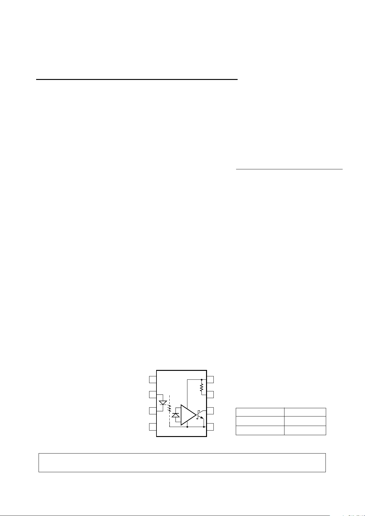
8
7
6
1
3
SHIELD
5
2
4
20 kΩ
Schematic Diagram
Truth Table
LED V
O
ON L
OFF H
5964-9648E
1-499
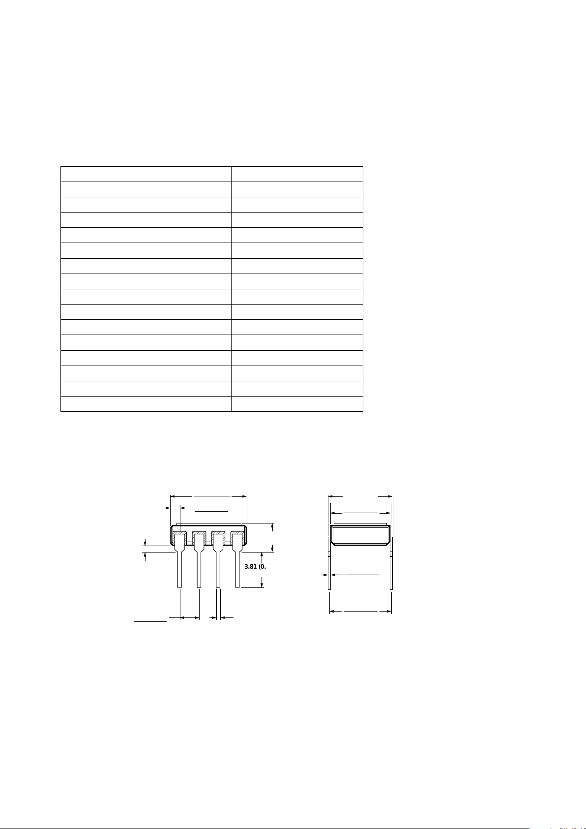
Selection Guide-Package Styles and Lead
Configuration Options
HP Part # and Options
Commercial HCPL-5300
MIL-PRF-38534, Class H HCPL-5301
MIL-PRF-38534, Class K HCPL-530K
Standard Lead Finish Gold Plate
Solder Dipped Option #200
Butt Cut/Gold Plate Option #100
Gull Wing/Soldered Option #300
SMD Part #
Prescript for all below 5962-
Either Gold or Solder 9685201HPX
Gold Plate 9685201HPC
Solder Dipped 9685201HPA
Butt Cut/Gold Plate 9685201HYC
Butt Cut/Soldered 9685201HYA
Gull Wing/Soldered 9685201HXA
Outline Drawing
3.81 (0.150)
MIN.
4.32 (0.170)
MAX.
9.40 (0.370)
9.91 (0.390)
0.51 (0.020)
MAX.
2.29 (0.090)
2.79 (0.110)
0.51 (0.020)
MIN.
0.76 (0.030)
1.27 (0.050)
8.13 (0.320)
MAX.
7.36 (0.290)
7.87 (0.310)
0.20 (0.008)
0.33 (0.013)
7.16 (0.282)
7.57 (0.298)
NOTE: DIMENSIONS IN MILLIMETERS (INCHES).
1-500
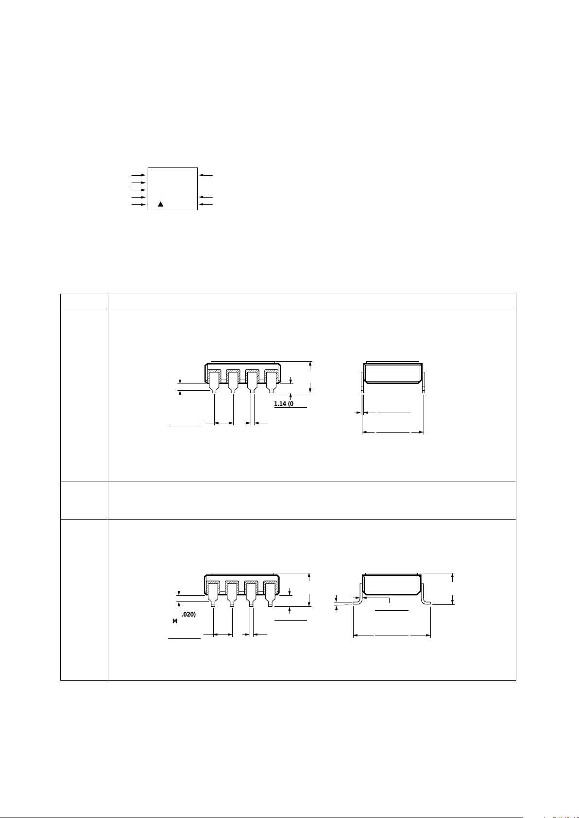
Device Marking
Hermetic Optocoupler Options
Option Description
100 Surface mountable hermetic optocoupler with leads trimmed for butt joint assembly. This
option is available on commercial and hi-rel product in 8 pin DIP (see drawings below for
details).
200 Lead finish is solder dipped rather than gold plated. This option is available on commercial
and hi-rel product in 8 pin DIP. DESC Drawing part numbers contain provisions for lead
finish.
300 Surface mountable hermetic optocoupler with leads cut and bent for gull wing assembly.
This option is available on commercial and hi-rel product in 8 pin DIP (see drawings below
for details). This option has solder dipped leads.
1.14 (0.045)
1.40 (0.055)
4.32 (0.170)
MAX.
0.51 (0.020)
MAX.
2.29 (0.090)
2.79 (0.110)
0.51 (0.020)
MIN.
7.36 (0.290)
7.87 (0.310)
0.20 (0.008)
0.33 (0.013)
NOTE: DIMENSIONS IN MILLIMETERS (INCHES).
COMPLIANCE INDICATOR,*
DATE CODE, SUFFIX (IF NEEDED)
HP QYYWWZ
XXXXXX
XXXXXXX
XXX USA
50434
COUNTRY OF MFR.
HP FSCN*
HP LOGO
DESC SMD*
PIN ONE/
ESD IDENT
HP P/N
DESC SMD*
* QUALIFIED PARTS ONLY
0.51 (0.020)
MIN.
5.57 (0.180)
MAX.
0.51 (0.020)
MAX.
2.29 (0.090)
2.79 (0.110)
1.40 (0.055)
1.65 (0.065)
9.65 (0.380)
9.91 (0.390)
5° MAX.
5.57 (0.180)
MAX.
0.20 (0.008)
0.33 (0.013)
NOTE: DIMENSIONS IN MILLIMETERS (INCHES).

1-501
Absolute Maximum Ratings
Storage Temperature (TS) ............................................................................................................. -65 to 150°C
Operating Temperature (TA) ......................................................................................................... -55 to 125°C
Junction Temperature (TJ) ...................................................................................................................... 175°C
Average Input Current (I
F(AVG)
) ............................................................................................................... 25 mA
Peak Input Current (50% duty cycle, ≤ 1 ms pulse width) (I
F(PEAK)
) ........................................................ 50 mA
Peak Transient Input Current (<1 µs pulse width, 300 pps) (I
F(TRAN)
) ..................................................... 1.0 A
Reverse Input Voltage (Pin 3-2) (VR)............................................................................................................ 5 V
Average Output Current (Pin 6) (I
O(AVG)
) ................................................................................................ 15 mA
Resistor Voltage (Pin 7) (V7) ......................................................................................................... -0.5 V to V
CC
Output Voltage (Pin 6-5) (VO) ........................................................................................................ -0.5 to 30 V
Supply Voltage (Pin 8-5) (VCC) ....................................................................................................... -0.5 to 30 V
Output Power Dissipation (PO)............................................................................................................. 100 mW
Total Power Dissipation (PT)................................................................................................................ 145 mW
Lead Solder Temperature (soldering, 10 seconds) .................................................................................. 260°C
ESD Classification
(MIL-STD-883, Method 3015)
HCPL-5300/5301 ......................(∆),Class 1
Recommended Operating Conditions
Parameter Symbol Min. Max. Units
Power Supply Voltage V
CC
4.5 30 Volts
Output Voltage V
O
0 30 Volts
Input Current (ON) I
F(ON)
10 20 mA
Input Voltage (OFF) V
F(OFF)
-5 0.8 V

1-502
Electrical Specifications
Over recommended operating conditions (TA = -55°C to +125°C, VCC = +4.5 V to 30 V,
I
F(ON)
= 10 mA to 20 mA, V
F(OFF)
= -5 V to 0.8 V) unless otherwise specified.
Group A
Sub-
Parameter Symbol groups
[12]
Min. Typ.* Max. Units Test Conditions Fig. Note
Current Transfer CTR 1, 2, 3 30 90 % IF = 10 mA, VO = 0.6 V 1
Ratio
Low Level Output I
OL
1, 2, 3 3.0 9.0 mA IF = 10 mA, VO = 0.6 V 1, 2
Current
Low Level Output V
OL
1, 2, 3 0.3 0.6 V IO = 2.4 mA
Input Threshold I
TH
1, 2, 3 1.5 5.0 mA VO = 0.8 V, 1 7
Current IO = 0.75 mA
High Level I
OH
1, 2, 3 5 75 µAVF = 0.8 V 3
Output Current
High Level Supply I
CCH
1, 2, 3 0.6 1.5 mA VF = 0.8 V, VO = Open 7
Current
Low Level Supply I
CCL
1, 2, 3 0.6 1.5 mA IF = 10 mA, VO = Open 7
Current
Input Forward V
F
1, 2, 3 1.0 1.5 1.8 V IF = 10 mA 4
Voltage
Temperature ∆VF/ -1.6 mV/°CIF = 10 mA
Coefficient of ∆T
A
Forward Voltage
Input Reverse BV
R
1, 2, 3 5 V IR = 100 µA
Breakdown Voltage
Input Capacitance C
IN
90 pF f = 1 MHz, VF = 0 V
Input-Output I
I-O
1 1.0 µA RH = 45%, t = 5 sec, 2
Insulation Leakage V
I-O
= 1500 Vdc,
Current TA = 25° C
Resistance R
I-O
10
12
Ω V
I-O
= 500 Vdc 2
(Input-Output)
Capacitance C
I-O
2.4 pF f = 1 MHz 2
(Input-Output)
Internal Pull-up R
L
1 142028kΩTA = 25° C 4, 5,
Resistor 6
Internal Pull-up ∆RL/ 0.014 kΩ/°C
Resistor ∆T
A
Temperature
Coefficient
*All typical values at 25°C, VCC = 15 V.
Voltage

1-503
Switching Specifications (R
L
= 20 kΩ External)
Over recommended operating conditions:
(TA = -55°C to +125°C, V
CC
= +4.5 V to 30 V, I
F(ON)
= 10 mA to 20 mA, V
F(OFF)
= -5 V to 0.8 V) unless
otherwise specified.
Group A
Parameter Symbol Subgrps.
[12]
Min. Typ.* Max. Units Test Conditions Fig. Note
Propagation t
PHL
9, 10, 11 30 180 450 ns CL =I
F(on)
= 10 mA, 5, 7, 3, 4,
Delay Time to 100 pF V
F(off)
= 0.8 V, 9-12 5, 6,
Low Output 100 ns C
L
=7
Level 10 pF
Propagation t
PLH
9, 10, 11 250 350 650 ns CL =
Delay Time to 100 pF
High Output 130 C
L
=
Level 10 pF
Pulse Width PWD 9, 10, 11 150 450 ns CL =11
Distortion 100 pF
Propagation t
PLH
- 9, 10, 11 -170 140 500 ns 8
Delay t
PHL
Difference
Between Any
Two Parts
Output High |CMH| 9 10 17 kV/µsIF = 0 mA, VCC = 15.0 V, 6, 17, 9, 13
Level Common V
O
> 3.0 V CL = 100 pF, 18, 21
Mode V
CM
= 1000 V
P-P
Immunity TA = 25°C
Transient
Output Low |CML| 9 10 17 kV/µsIF = 10 mA 10, 13
Level Common V
O
< 1.0 V
Mode
Transient
Immunity
*All typical values at 25°C, VCC = 15 V.
VCC = 15.0 V,
V
THLH
= 2.0 V,
V
THHL
= 1.5 V

1-504
Switching Specifications (RL= Internal Pull-up)
Over recommended operating conditions:
(TA = -55°C to +125°C, V
CC
= +4.5 V to 30 V, I
F(ON)
= 10 mA to 20 mA, V
F(OFF)
= -5 V to 0.8 V) unless
otherwise specified.
Group A
Parameter Symbol Subgrps.
[12]
Min. Typ.* Max. Units Test Conditions Fig. Note
Propagation t
PHL
9, 10, 11 20 185 500 ns I
F(on)
= 10 mA, 5, 8, 3, 4,
Delay Time to V
F(off)
= 0.8 V, 5, 6,
Low Output V
CC
= 15.0 V, 7
Level C
L
= 100 pF,
Propagation t
PLH
9, 10, 11 220 415 750 ns
Delay Time to
High Output
Level
Pulse Width PWD 9, 10, 11 150 600 ns 11
Distortion
Propagation t
PLH
- 9, 10, 11 -225 150 650 ns 8
Delay t
PHL
Difference
Between Any
Two Parts
Output High |CMH|10kV/µsIF = 0 mA, VCC = 15.0 V, 6, 21 9
Level Common V
O
> 3.0 V CL = 100 pF,
Mode Transient V
CM
= 1000
Immunity T
A
= 25°C
Output Low |CML|10kV/µsIF = 16 mA 10
Level Common V
O
< 1.0 V
Mode Transient
Immunity
Power Supply PSR 1.0 V
P-P
Square Wave, t
RISE
, t
FALL
7
Rejection > 5 ns, no bypass
capacitors.
*All typical values at 25°C, VCC = 15 V.
Notes:
1. CURRENT TRANSFER RATIO in percent is defined as the ratio of output collector current (IO) to the forward LED input current
(IF) times 100.
2. Device considered a two-terminal device: Pins 1, 2, 3 and 4 shorted together and Pins 5, 6, 7 and 8 shorted together.
3. Pulse: f = 20 kHz, Duty Cycle = 10%
4. The internal 20 kΩ resistor can be used by shorting pins 6 and 7 together.
5. Due to the tolerance of the internal resistor, and since propagation delay is dependent on the load resistor value, performance can
be improved by using an external 20 kΩ 1% load resistor. For more information on how propagation delay varies with load
resistance, see Figure 8.
6. The RL = 20 kΩ, CL = 100 pF represents a typical IPM (Intelligent Power Module) load.
7. Use of a 0.1 µF bypass capacitor connected between pins 5 and 8 can improve performance by filtering power supply line noise.
8. The difference in t
PLH
and t
PHL
between any two parts under the same test condition. (See IPM Dead Time and Propagation Delay
Specifications section.)
9. Common mode transient immunity in a Logic High level is the maximum tolerable dVCM/dt of the common mode pulse, VCM, to
assure that the output will remain in a Logic High state (i.e., VO > 3.0 V).
10. Common mode transient immunity in a Logic Low level is the maximum tolerable dVCM/dt of the common mode pulse, VCM, to
assure that the output will remain in a Logic Low state (i.e., VO < 1.0 V).
11. Pulse Width Distortion (PWD) is defined as the difference between t
PLH
and t
PHL
for any given device.
12. Standard parts receive 100% testing at 25°C (Subgroups 1 and 9). Hi-Rel and SMD parts receive 100% testing at 25°C, +125°C,
and -55°C (Subgroups 1 and 9, 2 and 10, 3 and 11 respectively).
13. Parameters are tested as part of device initial characterization and after design and process changes. Parameters are guaranteed
to limits specified for all lots not specifically tested.
V
THLH
= 2.0 V
V
THHL
= 1.5 V

1-505
LED Drive Circuit
Considerations For Ultra
High CMR Performance
Without a detector shield, the
dominant cause of optocoupler
CMR failure is capacitive
coupling from the input side of
the optocoupler, through the
package, to the detector IC as
shown in Figure 14. The HCPL5300/5301 improves CMR
performance by using a detector
IC with an optically transparent
Faraday shield, which diverts the
capacitively coupled current away
from the sensitive IC circuitry.
However, this shield does not
eliminate the capacitive coupling
between the LED and the optocoupler output pins and output
ground as shown in Figure 15.
This capacitive coupling causes
perturbations in the LED current
during common mode transients
and becomes the major source of
CMR failures for a shielded
optocoupler. The main design
objective of a high CMR LED
drive circuit becomes keeping the
LED in the proper state (on or
off) during common mode
transients. For example, the
recommended application circuit
(Figure 13), can achieve 10 kV/µs
CMR while minimizing component complexity. Note that a
CMOS gate is recommended in
Figure 13 to keep the LED off
when the gate is in the high state.
Another cause of CMR failure for
a shielded optocoupler is direct
coupling to the optocoupler
output pins through C
LEDO1
and
C
LEDO2
in Figure 15. Many factors
influence the effect and magnitude of the direct coupling
including: the use of an internal
or external output pull-up
resistor, the position of the LED
current setting resistor, the
connection of the unused input
package pins, and the value of
the capacitor at the optocoupler
output (CL).
Techniques to keep the LED in
the proper state and minimize the
effect of the direct coupling are
discussed in the next two
sections.
CMR With The LED On
(CMRL)
A high CMR LED drive circuit
must keep the LED on during
common mode transients. This is
achieved by overdriving the LED
current beyond the input
threshold so that it is not pulled
below the threshold during a
transient. The recommended
minimum LED current of 10 mA
provides adequate margin over
the maximum ITH of 5.0 mA (see
Figure 1) to achieve 10 kV/µs
CMR. Capacitive coupling is
higher when the internal load
resistor is used (due to C
LEDO2
)
and an IF= 16mA is required to
obtain 10 kV/µs CMR.
The placement of the LED
current setting resistor affects the
ability of the drive circuit to keep
the LED on during transients and
interacts with the direct coupling
to the optocoupler output. For
example, the LED resistor in
Figure 16 is connected to the
anode. Figure 17 shows the AC
equivalent circuit for Figure 16
during common mode transients.
During a +dV
CM/dt
in Figure 17,
the current available at the LED
anode (I
TOTAL
) is limited by the
series resistor. The LED current
(IF) is reduced from its DC value
by an amount equal to the current
that flows through C
LEDP
and
C
LEDO1
. The situation is made
worse because the current
through C
LEDO1
has the effect of
trying to pull the output high
(toward a CMR failure) at the
same time the LED current is
being reduced. For this reason,
the recommended LED drive
circuit (Figure 13) places the
current setting resistor in series
with the LED cathode. Figure 18
is the AC equivalent circuit for
Figure 13 during common mode
transients. In this case, the LED
current is not reduced during a
+dV
CM/dt
transient because the
current flowing through the
package capacitance is supplied
by the power supply. During a
-dV
CM/dt
transient, however, the
LED current is reduced by the
amount of current flowing
through C
LEDN
. But better CMR
performance is achieved since the
current flowing in C
LEDO1
during
a negative transient acts to keep
the output low.
Coupling to the LED and output
pins is also affected by the
connection of pins 1 and 4. If
CMR is limited by perturbations
in the LED on current, as it is for
the recommended drive circuit
(Figure 13), pins 1 and 4 should
be connected to the input circuit
common. However, if CMR
performance is limited by direct
coupling to the output when the
LED is off, pins 1 and 4 should
be left unconnected.
CMR With The LED Off
(CMRH)
A high CMR LED drive circuit
must keep the LED off
(VF≤ V
F(OFF)
) during common
mode transients. For example,
during a +dV
CM/dt
transient in
Figure 18, the current flowing
through C
LEDN
is supplied by the
parallel combination of the LED
and series resistor. As long as the
voltage developed across the
resistor is less than V
F(OFF)
the
LED will remain off and no

1-506
common mode failure will occur.
Even if the LED momentarily
turns on, the 100 pF capacitor
from pins 6-5 will keep the
output from dipping below the
threshold. The recommended
LED drive circuit (Figure 13)
provides about 10 V of margin
between the lowest optocoupler
output voltage and a 3 V IPM
threshold during a 10 kV/µs
transient with VCM= 1000 V.
Additional margin can be
obtained by adding a diode in
parallel with the resistor, as
shown by the dashed line connection in Figure 18, to clamp the
voltage across the LED below
V
F(OFF)
.
Since the open collector drive
circuit, shown in Figure 19,
cannot keep the LED off during a
+dV
CM/dt
transient, it is not
desirable for applications
requiring ultra high CMR
H
performance. Figure 20 is the AC
equivalent circuit for Figure 16
during common mode transients.
Essentially all the current flowing
through C
LEDN
during a +dV
CM/dt
transient must be supplied by the
LED. CMRH failures can occur at
dv/dt rates where the current
through the LED and C
LEDN
exceeds the input threshold.
Figure 21 is an alternative drive
circuit which does achieve ultra
high CMR performance by
shunting the LED in the off state.
IPM Dead Time and
Propagation Delay
Specifications
These devices include a
Propagation Delay Difference
specification intended to help
designers minimize “dead time” in
their power inverter designs.
Dead time is the time period
during which both the high and
low side power transistors (Q1
and Q2 in Figure 22) are off. Any
overlap in Q1 and Q2 conduction
will result in large currents
flowing through the power
devices between the high and low
voltage motor rails.
To minimize dead time the
designer must consider the
propagation delay characteristics
of the optocoupler as well as the
characteristics of the IPM IGBT
gate drive circuit. Considering
only the delay characteristics of
the optocoupler (the characteristics of the IPM IGBT gate drive
circuit can be analyzed in the
same way) it is important to
know the minimum and maximum
turn-on (t
PHL
) and turn-off (t
PLH
)
propagation delay specifications,
preferably over the desired
operating temperature range.
The limiting case of zero dead
time occurs when the input to Q1
turns off at the same time that the
input to Q2 turns on. This case
determines the minimum delay
between LED1 turn-off and LED2
turn-on, which is related to the
worst case optocoupler propagation delay waveforms, as shown
in Figure 23. A minimum dead
time of zero is achieved in Figure
23 when the signal to turn on
LED2 is delayed by (t
PLH max
-
t
PHL min
) from the LED1 turn off.
This delay is the maximum value
for the propagation delay
difference specification which is
specified at 500 ns for the HCPL5300/5301 over an operating
temperature range of -55°C to
+125°C.
Delaying the LED signal by the
maximum propagation delay
difference ensures that the minimum dead time is zero, but it
does not tell a designer what the
maximum dead time will be. The
maximum dead time occurs in the
highly unlikely case where one
optocoupler with the fastest t
PLH
and another with the slowest t
PHL
are in the same inverter leg. The
maximum dead time in this case
becomes the sum of the spread in
the t
PLH
and t
PHL
propagation
delays as shown in Figure 24. The
maximum dead time is also
equivalent to the difference
between the maximum and
minimum propagation delay
difference specifications. The
maximum dead time (due to the
optocouplers) for the HCPL5300/5301 is 670 ns (= 500 ns (-170 ns)) over an operating
temperature range of -55°C to
+125°C.

1-507
I
O
– OUTPUT CURRENT – mA
0
IF – FORWARD LED CURRENT – mA
6
4
2
5
10
10 15 20
VO = 0.6 V
8
0
125 °C
25 °C
-55 °C
Figure 5. Propagation Delay Test Circuit.
Figure 1. Typical Transfer
Characteristics.
Figure 2. Normalized Output Current
vs. Temperature.
Figure 3. High Level Output Current
vs. Temperature.
0.1 µF
V
CC
= 15 V
20 k
Ω
I
F(ON)
=10 mA
V
OUT
CL*
+
–
*TOTAL LOAD CAPACITANCE
+
–
I
f
V
O
V
THHL
t
PHL
t
PLH
t
f
t
r
90%
10%
90%
10%
V
THLH
8
7
6
1
3
SHIELD
5
2
4
5 V
20 kΩ
I
F
– FORWARD CURRENT – mA
1.10
0.001
VF – FORWARD VOLTAGE – VOLTS
1.60
10
1.0
0.1
1.20
1000
1.30 1.40 1.50
TA = 25°C
I
F
V
F
+
–
0.01
100
Figure 4. Input Current vs. Forward
Voltage.
NORMALIZED OUTPUT CURRENT
TA – TEMPERATURE – °C
0.8
0.7
0.5
IF = 10 mA
V
O
= 0.6 V
0.9
1.0
0
0.6
0 40 60 100-60 -20 20 80-40 120 140
I
OH
– HIGH LEVEL OUTPUT CURRENT – µA
TA – TEMPERATURE – °C
20
10
5
25
0
VF = 0.8 V
V
CC
= VO = 30 V
15
0 40 60 100-60 -20 20 80-40 120140

1-508
t
P
– PROPAGATION DELAY – ns
TA – TEMPERATURE – °C
500
300
200
600
t
PLH
t
PHL
IF = 10 mA
V
CC
= 15 V
CL = 100 pF
RL = 20 kΩ
(INTERNAL)
100
0 40 60 100-60 -20 20 80-40 120140
400
Figure 11. Propagation Delay vs.
Supply Voltage.
Figure 10. Propagation Delay vs. Load
Capacitance.
t
P
– PROPAGATION DELAY – ns
0
CL – LOAD CAPACITANCE – pF
800
600
400
100
1400
200 300 400
IF = 10 mA
V
CC
= 15 V
RL = 20 kΩ
T
A
= 25°C
200
1000
t
PLH
t
PHL
1200
0 500
t
P
– PROPAGATION DELAY – ns
0
V
CC
– SUPPLY VOLTAGE – V
800
600
400
10
1400
15 20 25
IF = 10 mA
CL = 100 pF
RL = 20 kΩ
T
A
= 25°C
200
1000
t
PLH
t
PHL
530
1200
t
P
– PROPAGATION DELAY – ns
RL – LOAD RESISTANCE – K Ω
600
400
200
30 50
800
010
20
40
t
PLH
t
PHL
IF = 10 mA
V
CC
= 15 V
CL = 100 pF
T
A
= 25 °C
Figure 7. Propagation Delay with
External 20 kΩ RL vs. Temperature.
Figure 8. Propagation Delay with
Internal 20 kΩ RL vs. Temperature.
Figure 9. Propagation Delay vs. Load
Resistance.
Figure 6. CMR Test Circuit. Typical CMR Waveform.
V
CM
∆t
OV
V
O
V
O
SWITCH AT A: IF = 0 mA
SWITCH AT B: I
F
= 10 mA
V
CC
V
OL
V
CM
∆t
δV
δt
=
t
P
– PROPAGATION DELAY – ns
TA – TEMPERATURE – °C
500
300
200
600
t
PLH
t
PHL
IF = 10 mA
V
CC
= 15 V
CL = 100 pF
RL = 20 kΩ
(EXTERNAL)
100
0 40 60 100-60 -20 20 80-40 120140
400
0.1 µF
V
CC
= 15 V
20 kΩ
A
I
F
V
OUT
100 pF*
+
–
*100 pF TOTAL
CAPACITANCE
+
–
+
–
B
V
FF
V
CM
= 1000 V
8
7
6
1
3
SHIELD
5
2
4
20 kΩ

1-509
Figure 12. Propagation Delay vs. Input
Current.
t
P
– PROPAGATION DELAY – ns
100
IF – FORWARD LED CURRENT – mA
300
10
500
15
VCC = 15 V
CL = 100 pF
RL = 20 kΩ
T
A
= 25°C
200
400
t
PLH
t
PHL
5020
Figure 15. Optocoupler Input to
Output Capacitance Model for
Shielded Optocouplers.
Figure 16. LED Drive Circuit with Resistor Connected to LED Anode (Not
Recommended).
8
7
6
1
3
SHIELD
5
2
4
C
LEDP
C
LEDN
C
LED01
C
LED02
20 kΩ
0.1 µF
V
CC
= 15 V
20 kΩ
CMOS
310 Ω
+5 V
V
OUT
100 pF
+
–
*100 pF TOTAL
CAPACITANCE
8
7
6
1
3
SHIELD
5
2
4
20 kΩ
Figure 13. Recommended LED Drive Circuit. Figure 14. Optocoupler Input to
Output Capacitance Model for
Unshielded Optocouplers.
0.1 µF
V
CC
= 15 V
20 kΩ
CMOS
310 Ω
+5 V
V
OUT
100 pF
+
–
*100 pF TOTAL
CAPACITANCE
8
7
6
1
3
SHIELD
5
2
4
20 kΩ
8
7
6
1
3
SHIELD
5
2
4
C
LEDP
C
LEDN
20 kΩ

1-510
Figure 21. Recommended LED Drive
Circuit for Ultra High CMR.
+5 V
8
7
6
1
3
SHIELD
5
2
4
20 kΩ
20 kΩ
* THE ARROWS INDICATE THE DIRECTION OF CURRENT
FLOW FOR +dV
CM
/dt TRANSIENTS.
300 Ω
V
OUT
100 pF
+
–
I
TOTAL*
V
CM
8
7
6
1
3
SHIELD
5
2
4
20
kΩ
C
LEDN
C
LED01
C
LED02
I
CLEDP
I
F
C
LEDP
I
CLED01
20 kΩ
* THE ARROWS INDICATE THE DIRECTION OF CURRENT
FLOW FOR +dV
CM
/dt TRANSIENTS.
** OPTIONAL CLAMPING DIODE FOR IMPROVED CMH
PERFORMANCE. V
R
< V
F (OFF)
DURING +dVCM/dt.
V
OUT
100 pF
+
–
V
CM
8
7
6
1
3
SHIELD
5
2
4
20
kΩ
C
LEDP
C
LEDN
C
LED01
C
LED02
I
CLEDN*
300 Ω
+ VR** –
Figure 17. AC Equivalent Circuit for
Figure 16 During Common Mode
Transients.
Figure 18. AC Equivalent Circuit for Figure 13 During
Common Mode Transients.
Figure 19. Not Recommended Open Collector LED Drive
Circuit.
Q1
+5 V
8
7
6
1
3
SHIELD
5
2
4
20 kΩ
20 kΩ
* THE ARROWS INDICATE THE DIRECTION OF CURRENT
FLOW FOR +dV
CM
/dt TRANSIENTS.
V
OUT
100 pF
+
–
V
CM
8
7
6
1
3
SHIELD
5
2
4
20
kΩ
C
LEDP
C
LEDN
C
LED01
C
LED02
I
CLEDN*
Q1
Figure 20. AC Equivalent Circuit for Figure 19 During
Common Mode Transients.

1-511
0.1 µF
20 kΩ
CMOS
310 Ω
+5 V
V
OUT1
I
LED1
V
CC1
M
HCPL-5300
HCPL-5300
HCPL-5300
HCPL-5300
HCPL-5300
Q2
Q1
-HV
+HV
IPM
8
7
6
1
3
SHIELD
5
2
4
20 k
Ω
HCPL-5300
0.1 µF
20 kΩ
CMOS
310 Ω
+5 V
V
OUT2
I
LED2
V
CC2
8
7
6
1
3
SHIELD
5
2
4
20 k
Ω
HCPL-5300
Figure 22. Typical Application Circuit.
Figure 24. Waveforms for Dead Time Calculations.
V
OUT1
V
OUT2
I
LED2
t
PLH
MIN.
MAXIMUM DEAD TIME
(DUE TO OPTOCOUPLER)
= (t
PLH MAX.
-
t
PLH MIN.
) + (t
PHL MAX.
-
t
PHL MIN.
)
= (t
PLH MAX.
-
t
PHL MIN.
) - (t
PLH MIN.
-
t
PHL MAX.
)
= PDD* MAX. - PDD* MIN.
t
PHL
MIN.
I
LED1
Q1 ON
Q2 OFF
Q1 OFF
Q2 ON
*PDD = PROPAGATION DELAY DIFFERENCE
t
PLH
MAX.
t
PHL
MAX.
PDD*
MAX.
MAX.
DEAD TIME
NOTE: THE PROPAGATION DELAYS USED TO CALCULATE THE MAXIMUM
DEAD TIME ARE TAKEN AT EQUAL TEMPERATURES.
Figure 23. Minimum LED Skew for
Zero Dead Time.
V
OUT1
V
OUT2
I
LED2
t
PLH MAX.
PDD* MAX. =
(t
PLH-tPHL) MAX. = tPLH MAX. - tPHL MIN.
t
PHL
MIN.
I
LED1
Q1 ON
Q2 OFF
Q1 OFF
Q2 ON
*PDD = PROPAGATION DELAY DIFFERENCE
NOTE: THE PROPAGATION DELAYS USED TO CALCULATE
PDD ARE TAKEN AT EQUAL TEMPERATURES.
MIL-PRF-38534 Class H,
Class K, and DESC SMD
Test Program
Hewlett-Packard’s Hi-Rel Optocouplers are in compliance with
MIL-PRF-38534 Classes H and K.
Class H devices are also in
compliance with DESC drawing
5962-96852.
Testing consists of 100% screening and quality conformance
inspection to MIL-PRF-38534.
 Loading...