

HP HCPL-5401, HCPL-5400, HCPL-543K, HCPL-643K, HCPL-6431 Datasheet
...
1-524
V
CC
V
O
V
E
GND
H
Hermetically Sealed,
Very High Speed,
Logic Gate Optocouplers
Technical Data
Features
• Dual Marked with Device
Part Number and DESC
Drawing Number
• Manufactured and Tested on
a MIL-PRF-38534 Certified
Line
• QML-38534, Class H and K
• Three Hermetically Sealed
Package Configurations
• Performance Guaranteed
over -55°C to +125°C
• High Speed: 40 M bit/s
• High Common Mode
Rejection 500 V/µs
Guaranteed
• 1500 Vdc Withstand Test
Voltage
• Active (Totem Pole) Outputs
• Three Stage Output Available
• High Radiation Immunity
• HCPL-2400/30 Function
Compatibility
• Reliability Data
• Compatible with TTL, STTL,
LSTTL, and HCMOS Logic
Families
Applications
• Military and Space
• High Reliability Systems
• Transportation, Medical, and
Life Critical Systems
• Isolation of High Speed
Logic Systems
Each channel contains an AlGaAs
light emitting diode which is
optically coupled to an integrated
high gain photon detector. This
combination results in very high
HCPL-540X*
5962-89570
HCPL-543X
Functional Diagram
Multiple Channel Devices
Available
Single Channel DIP
Input Enable Output
On (H) L L
Off (L) L H
On (H) H Z
Off (L) H Z
Truth Tables
(Positive Logic)
Multichannel Devices
Input Output
On (H) H
Off (L) L
HCPL-643X
5962-89571
*See matrix for available extensions.
• Computer-Peripheral
Interfaces
• Switching Power Supplies
• Isolated Bus Driver
(Networking Applications)(5400/1 Only)
• Pulse Transformer
Replacement
• Ground Loop Elimination
• Harsh Industrial
Environments
• High Speed Disk Drive I/O
• Digital Isolation for A/D,
D/A Conversion
Description
These units are single and dual
channel, hermetically sealed
optocouplers. The products are
capable of operation and storage
over the full military temperature
range and can be purchased as
either standard product or with
full MIL-PRF-38534 Class Level
H or K testing or from the
appropriate DESC Drawing. All
devices are manufactured and
tested on a MIL-PRF-38534
certified line and are included in
the DESC Qualified Manufacturers List QML-38534 for Hybrid
Microcircuits.
CAUTION: It is advised that normal static precautions be taken in handling and assembly of this component to
prevent damage and/or degradation which may be induced by ESD.
5965-3004E

1-525
Selection Guide–Package Styles and Lead Configuration Options
Package 8 Pin DIP 8 Pin DIP 20 Pad LCCC
Lead Style Through Hole Through Hole Surface Mount
Channels 1 2 2
Common Channel None VCC, GND None
Wiring
HP Part # & Options
Commercial HCPL-5400 HCPL-5430 HCPL-6430
MIL-PRF-38534, Class H HCPL-5401 HCPL-5431 HCPL-6431
MIL-PRF-38534, Class K HCPL-540K HCPL-543K HCPL-643K
Standard Lead Finish Gold Plate Gold Plate Solder Pads
Solder Dipped Option #200 Option #200
Butt Cut/Gold Plate Option #100 Option #100
Gull Wing/Soldered Option #300 Option #300
SMD Part #
Prescript for all below 5962- 5962- 5962Either Gold or Solder 8957001PX 8957101PX 89571022X
Gold Plate 8957001PC 8957101PC
Solder Dipped 8957001PA 8957101PA 89571022A
Butt Cut/Gold Plate 8957001YC 8957101YC
Butt Cut/Soldered 8957001YA 8957101YA
Gull Wing/Soldered 8957001XA 8957101XA
data rate capability. The detector
has a threshold with hysteresis,
which typically provides 0.25 mA
of differential mode noise
immunity and minimizes the
potential for output signal
chatter. The detector in the single
channel units has a three state
output stage which eliminates the
need for a pull-up resistor and
allows for direct drive of a data
bus.
All units are compatible with TTL,
STTL, LSTTL, and HCMOS logic
families. The 35 ns pulse width
distortion specification guarantees a 10 MBd signaling rate at
+125°C with 35% pulse width
distortion. Figures 13 through 16
show recommended circuits for
reducing pulse width distortion
and optimizing the signal rate of
the product. Package styles for
these parts are 8 pin DIP through
hole (case outlines P), and
leadless ceramic chip carrier
(case outline 2). Devices may be
purchased with a variety of lead
bend and plating options. See
Selection Guide Table for details.
Standard Military Drawing (SMD)
parts are available for each
package and lead style.
Because the same electrical die
(emitters and detectors) are used
for each channel of each device
listed in this data sheet, absolute
maximum ratings, recommended
operating conditions, electrical
specifications, and performance
characteristics shown in the
figures are similar for all parts.
Occasional exceptions exist due
to package variations and limitations and are as noted. Additionally, the same package assembly
processes and materials are used
in all devices. These similarities
give justification for the use of
data obtained from one part to
represent other part’s performance for die related reliability and
certain limited radiation test
results.
1-526
7
5
6
8
1
2
3
4
V
CC
GND
V
E
V
O
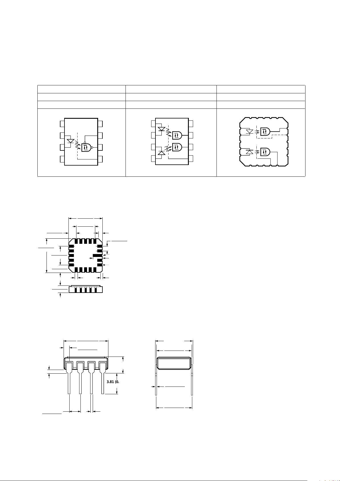
Functional Diagrams
8 Pin DIP 8 Pin DIP 20 Pad LCCC
Through Hole Through Hole Surface Mount
1 Channel 2 Channels 2 Channels
Note: All DIP devices have common VCC and ground. LCCC (leadless ceramic chip carrier) package has isolated channels with
separate VCC and ground connections.
Outline Drawings
V
CC
7
5
6
8
V
O1
GND
1
2
3
4
V
O2
GND
1
V
O2
19
20
2
3
V
O1
87
V
CC2
V
CC1
10
GND
2
15
13
12
20 Terminal LCCC Surface Mount, 2 Channels
8.70 (0.342)
9.10 (0.358)
4.95 (0.195)
5.21 (0.205)
1.78 (0.070)
2.03 (0.080)
1.02 (0.040) (3 PLCS)
4.95 (0.195)
5.21 (0.205)
8.70 (0.342)
9.10 (0.358)
1.78 (0.070)
2.03 (0.080)
0.51 (0.020)
0.64
(0.025)
(20 PLCS)
1.52 (0.060)
2.03 (0.080)
METALIZED
CASTILLATIONS (20 PLCS)
2.16 (0.085)
TERMINAL 1 IDENTIFIER
NOTE: DIMENSIONS IN MILLIMETERS (INCHES).
SOLDER THICKNESS 0.127 (0.005) MAX.
1.14 (0.045)
1.40 (0.055)
3.81 (0.150)
MIN.
4.32 (0.170)
MAX.
9.40 (0.370)
9.91 (0.390)
0.51 (0.020)
MAX.
2.29 (0.090)
2.79 (0.110)
0.51 (0.020)
MIN.
0.76 (0.030)
1.27 (0.050)
8.13 (0.320)
MAX.
7.36 (0.290)
7.87 (0.310)
0.20 (0.008)
0.33 (0.013)
7.16 (0.282)
7.57 (0.298)
NOTE: DIMENSIONS IN MILLIMETERS (INCHES).
8 Pin DIP Through Hole, 1 and 2 Channel

1-527
0.51 (0.020)
MIN.
5.57 (0.180)
MAX.
0.51 (0.020)
MAX.
2.29 (0.090)
2.79 (0.110)
1.40 (0.055)
1.65 (0.065)
9.65 (0.380)
9.91 (0.390)
5° MAX.
5.57 (0.180)
MAX.
0.20 (0.008)
0.33 (0.013)
NOTE: DIMENSIONS IN MILLIMETERS (INCHES).
Leadless Device MarkingLeaded Device Marking
Hermetic Optocoupler Options
Option Description
100 Surface mountable hermetic optocoupler with leads trimmed for butt joint assembly. This
option is available on commercial and hi-rel product in 8 pin DIP (see drawings below for
details).
200 Lead finish is solder dipped rather than gold plated. This option is available on commercial
and hi-rel product in 8 pin DIP. DESC Drawing part numbers contain provisions for lead
finish. All leadless chip carrier devices are delivered with solder dipped terminals as a
standard feature.
300 Surface mountable hermetic optocoupler with leads cut and bent for gull wing assembly. This
option is available on commercial and hi-rel product in 8 pin DIP (see drawings below for
details). This option has solder dipped leads.
1.14 (0.045)
1.40 (0.055)
4.32 (0.170)
MAX.
0.51 (0.020)
MAX.
2.29 (0.090)
2.79 (0.110)
0.51 (0.020)
MIN.
7.36 (0.290)
7.87 (0.310)
0.20 (0.008)
0.33 (0.013)
NOTE: DIMENSIONS IN MILLIMETERS (INCHES).
COMPLIANCE INDICATOR,*
DATE CODE, SUFFIX (IF NEEDED)
HP QYYWWZ
XXXXXX
XXXXXXX
XXX USA
* 50434
COUNTRY OF MFR.
HP FSCN*
HP LOGO
DESC SMD*
PIN ONE/
ESD IDENT
HP P/N
DESC SMD*
* QUALIFIED PARTS ONLY
COMPLIANCE INDICATOR,*
DATE CODE, SUFFIX (IF NEEDED)
HP QYYWWZ
XXXXXX
* XXXX
XXXXXX
USA 50434
DESC SMD*
HP FSCN*
HP LOGO
COUNTRY OF MFR.
HP P/N
PIN ONE/
ESD IDENT
DESC SMD*
* QUALIFIED PARTS ONLY
 Loading...