

Page 1
µA7800 SERIES
POSITIVE-VOLTAGE REGULATORS
SLVS056E – MAY 1976 – REVISED JULY 1999
D
3-Terminal Regulators
D
Output Current up to 1.5 A
D
Internal Thermal-Overload Protection
D
High Power-Dissipation Capability
D
Internal Short-Circuit Current Limiting
D
Output Transistor Safe-Area Compensation
D
Direct Replacements for Fairchild µA7800
Series
description
This series of fixed-voltage monolithic
integrated-circuit voltage regulators is designed
for a wide range of applications. These
applications include on-card regulation for
elimination of noise and distribution problems
associated with single-point regulation. Each of
these regulators can deliver up to 1.5 A of output
current. The internal current-limiting and
thermal-shutdown features of these regulators
essentially make them immune to overload. In
addition to use as fixed-voltage regulators, these
devices can be used with external components to
obtain adjustable output voltages and currents,
and also can be used as the power-pass element
in precision regulators.
The µA7800C series is characterized for
operation over the virtual junction temperature
range of 0°C to 125°C.
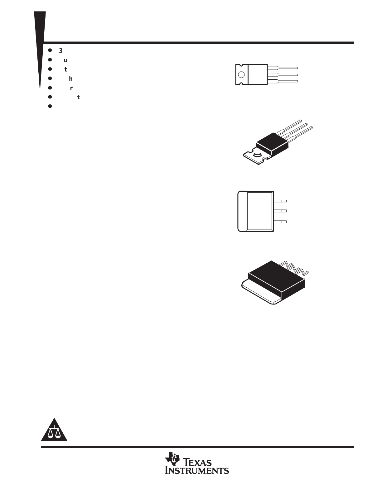
KC PACKAGE
(TOP VIEW)
OUTPUT
COMMON
INPUT
The COMMON terminal is in electrical
contact with the mounting base.
TO-220AB
O
C
I
KTE PACKAGE
(TOP VIEW)
OUTPUT
COMMON
INPUT
The COMMON terminal is in
electrical contact with the mounting
base.
O
C
I
Please be aware that an important notice concerning availability, standard warranty, and use in critical applications of
Texas Instruments semiconductor products and disclaimers thereto appears at the end of this data sheet.
PRODUCTION DATA information is current as of publication date.
Products conform to specifications per the terms of Texas Instruments
standard warranty. Production processing does not necessarily include
testing of all parameters.
POST OFFICE BOX 655303 • DALLAS, TEXAS 75265
Copyright 1999, Texas Instruments Incorporated
1
Page 2
µA7800 SERIES
CHIP
POSITIVE-VOLTAGE REGULATORS
SLVS056E – MAY 1976 – REVISED JULY 1999
V
O(NOM)
(V)
5 µA7805CKC µA7805CKTE µA7805Y
6 µA7806CKC µA7806CKTE µA7806Y
8 µA7808CKC µA7808CKTE µA7808Y
8.5 µA7885CKC µA7885CKTE µA7885Y
10 µA7810CKC µA7810CKTE µA7810Y
12 µA7812CKC µA7812CKTE µA7812Y
15 µA7815CKC µA7815CKTE µA7815Y
18 µA7818CKC µA7818CKTE µA7818Y
24 µA7824CKC µA7824CKTE µA7824Y
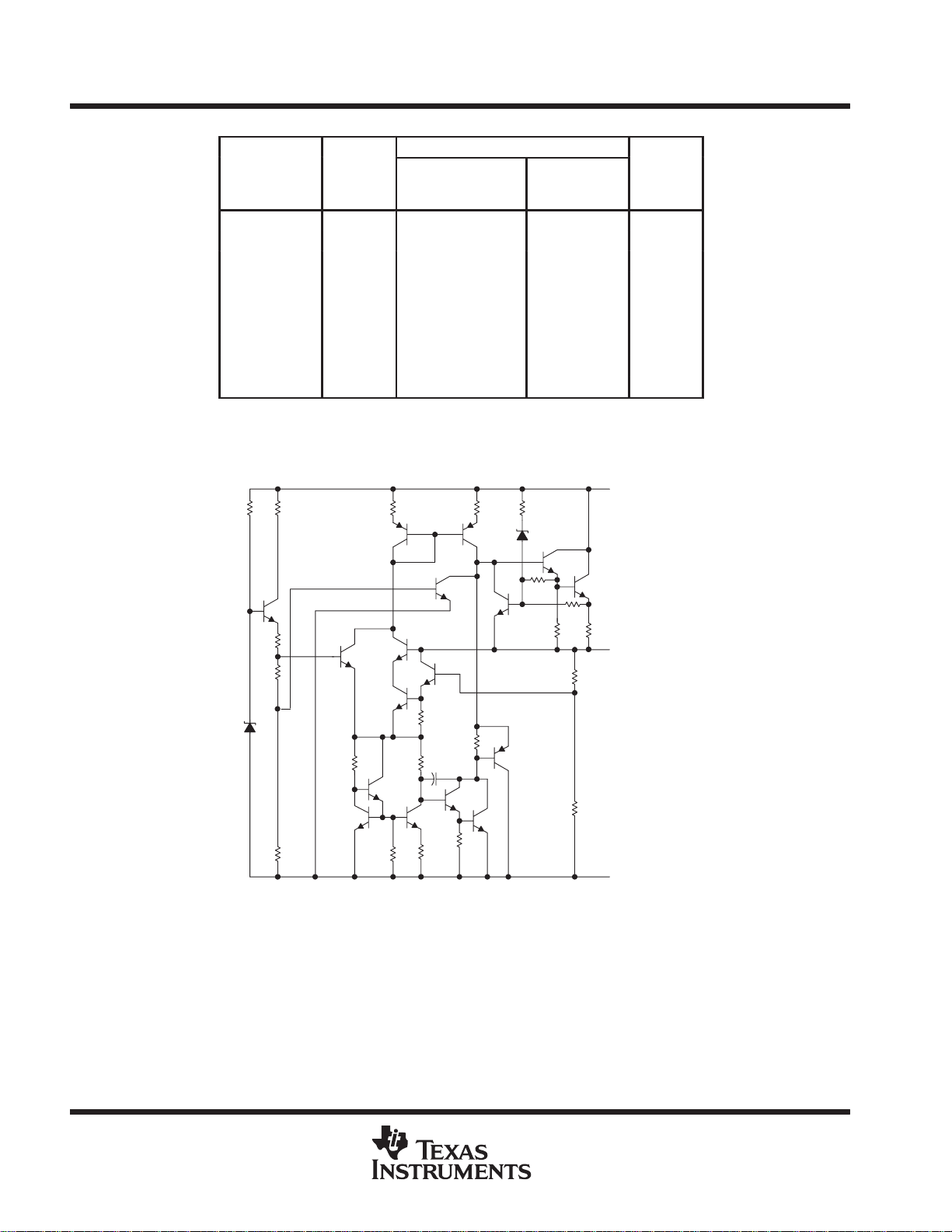
schematic
T
J
0°C to 125°C
The KTE package is only available taped and reeled. Add the suffix R to the device type
(e.g., µA7805CKTER). Chip forms are tested at 25°C.
AVAILABLE OPTIONS
PACKAGED DEVICES
PLASTIC
FLANGE-MOUNT
(KC)
HEAT-SINK
MOUNTED
(KTE)
FORM
(Y)
INPUT
OUTPUT
COMMON
2
POST OFFICE BOX 655303 • DALLAS, TEXAS 75265
Page 3
Input voltage, V
V
Package thermal impedance, θ
(see Notes 1 and 2)
°C
µA7800 SERIES
POSITIVE-VOLTAGE REGULATORS
SLVS056E – MAY 1976 – REVISED JULY 1999
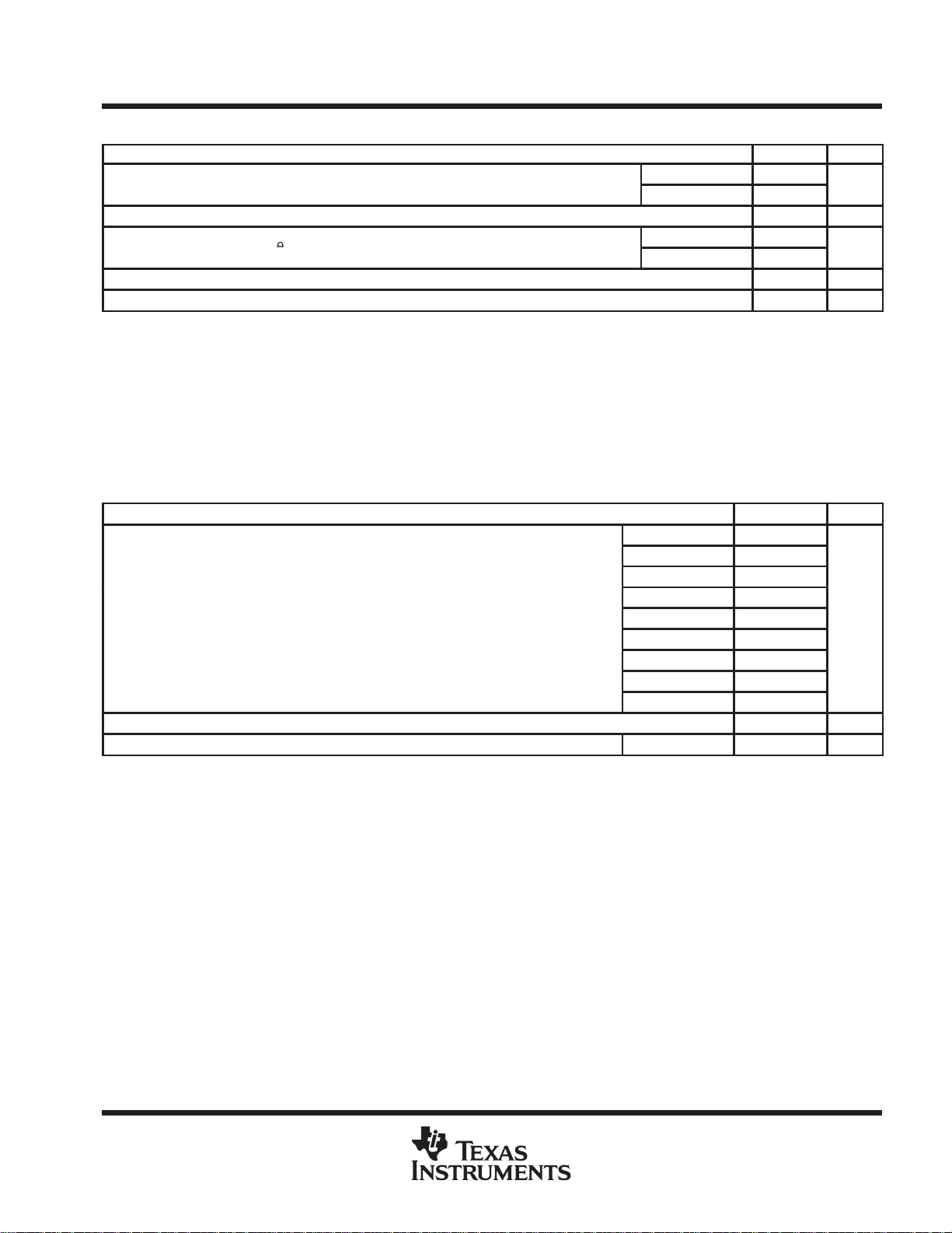
absolute maximum ratings over operating temperature ranges (unless otherwise noted)
µA78xx UNIT
p
Virtual junction temperature range, T
Lead temperature 1,6 mm (1/16 inch) from case for 10 seconds 260 °C
Storage temperature range, T
†
Stresses beyond those listed under “absolute maximum ratings” may cause permanent damage to the device. These are stress ratings only, and
functional operation of the device at these or any other conditions beyond those indicated under “recommended operating conditions” is not
implied. Exposure to absolute-maximum-rated conditions for extended periods may affect device reliability.
NOTES: 1. Maximum power dissipation is a function of TJ(max), θJA, and TA. The maximum allowable power dissipation at any allowable
I
J
p
ambient temperature is PD = (TJ(max) – TA)/θJA. Operating at the absolute maximum TJ of 150°C can impact reliability. Due to
variations in individual device electrical characteristics and thermal resistance, the built-in thermal overload protection may be
activated at power levels slightly above or below the rated dissipation.
2. The package thermal impedance is calculated in accordance with JESD 51, except for through-hole packages, which use a trace
length of zero.
stg
JA
µA7824C 40
All others 35
KC package 22
KTE package 23
–65 to 150 °C
†
0 to 150 °C
°
recommended operating conditions
MIN MAX UNIT
µA7805C 7 25
µA7806C 8 25
µA7808C 10.5 25
µA7885C 10.5 25
Input voltage, V
Output current, I
Operating virtual junction temperature, T
I
O
µA7810C 12.5 28
µA7812C 14.5 30
µA7815C 17.5 30
µA7818C 21 33
µA7824C 27 38
1.5 A
J
µA7800C series 0 125 °C
V
POST OFFICE BOX 655303 • DALLAS, TEXAS 75265
3
Page 4
µA7800 SERIES
PARAMETER
TEST CONDITIONS
T
†
UNIT
Output voltage
O
,
I
,
V
Input voltage regulation
25°C
mV
Output voltage regulation
25°C
mV
Bias current change
0°C
125°C
mA
PARAMETER
TEST CONDITIONS
T
†
UNIT
Output voltage
O
,
I
,
V
Input voltage regulation
25°C
mV
Output voltage regulation
25°C
mV
Bias current change
0°C to 125°C
mA
POSITIVE-VOLTAGE REGULATORS
SLVS056E – MAY 1976 – REVISED JULY 1999
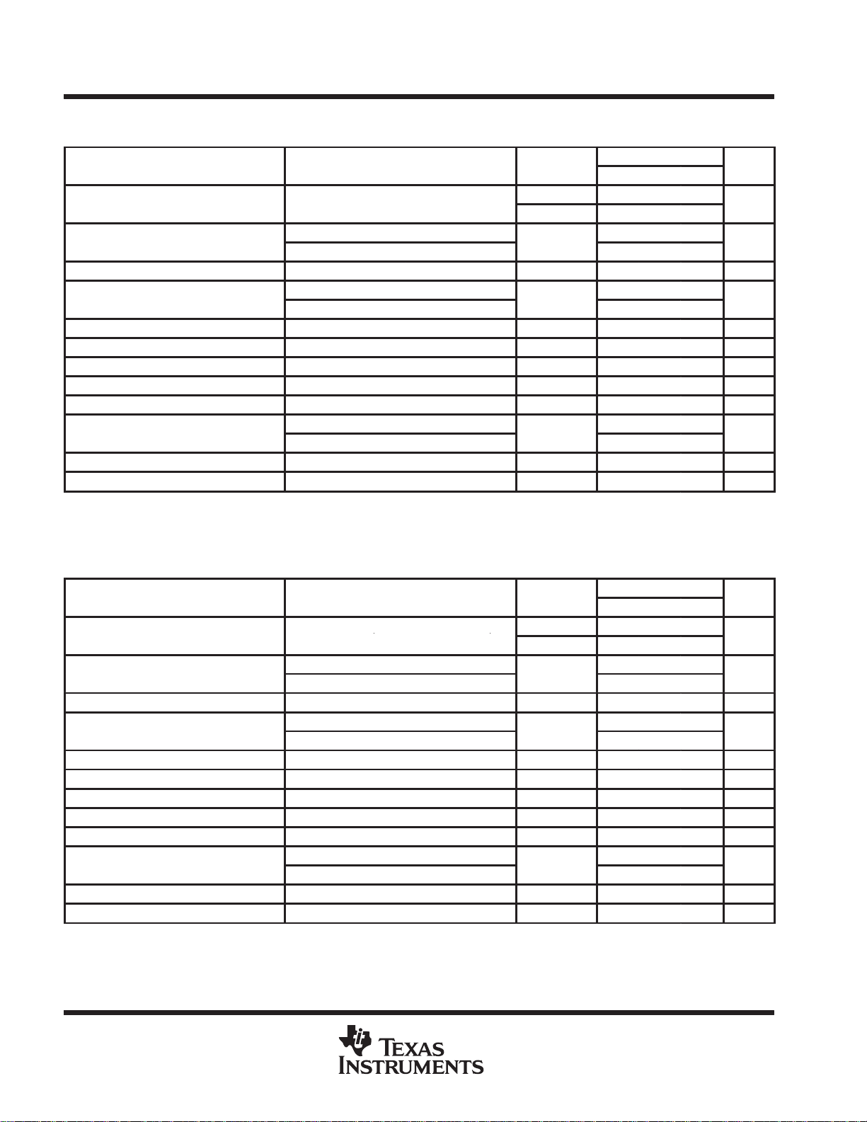
electrical characteristics at specified virtual junction temperature, VI = 10 V, IO = 500 mA (unless
otherwise noted)
J
I
p
p
Ripple rejection VI = 8 V to 18 V, f = 120 Hz 0°C to 125°C 62 78 dB
p
Output resistance f = 1 kHz 0°C to 125°C 0.017 Ω
Temperature coefficient of output voltage IO = 5 mA 0°C to 125°C –1.1 mV/°C
Output noise voltage f = 10 Hz to 100 kHz 25°C 40 µV
Dropout voltage IO = 1 A 25°C 2 V
Bias current 25°C 4.2 8 mA
Short-circuit output current 25°C 750 mA
Peak output current 25°C 2.2 A
†
Pulse-testing techniques maintain the junction temperature as close to the ambient temperature as possible. Thermal effects must be taken into
account separately . All characteristics are measured with a 0.33-µF capacitor across the input and a 0.1-µF capacitor across the output.
= 5 mA to 1 A, V
PD ≤ 15 W
VI = 7 V to 25 V
VI = 8 V to 12 V
IO = 5 mA to 1.5 A
IO = 250 mA to 750 mA
VI = 7 V to 25 V
IO = 5 mA to 1 A
= 7 V to 20 V,
25°C 4.8 5 5.2
0°C to 125°C 4.75 5.25
°
°
to
µA7805C
MIN TYP MAX
3 100
1 50
15 100
5 50
1.3
0.5
electrical characteristics at specified virtual junction temperature, VI = 11 V, IO = 500 mA (unless
otherwise noted)
J
I
p
p
Ripple rejection VI = 9 V to 19 V, f = 120 Hz 0°C to 125°C 59 75 dB
p
Output resistance f = 1 kHz 0°C to 125°C 0.019 Ω
Temperature coefficient of output voltage IO = 5 mA 0°C to 125°C –0.8 mV/°C
Output noise voltage f = 10 Hz to 100 kHz 25°C 45 µV
Dropout voltage IO = 1 A 25°C 2 V
Bias current 25°C 4.3 8 mA
Short-circuit output current 25°C 550 mA
Peak output current 25°C 2.2 A
†
Pulse-testing techniques maintain the junction temperature as close to the ambient temperature as possible. Thermal effects must be taken into
account separately . All characteristics are measured with a 0.33-µF capacitor across the input and a 0.1-µF capacitor across the output.
= 5 mA to 1 A, V
PD ≤ 15 W
VI = 8 V to 25 V
VI = 9 V to 13 V
IO = 5 mA to 1.5 A
IO = 250 mA to 750 mA
VI = 8 V to 25 V
IO = 5 mA to 1 A
= 8 V to 21 V,
25°C 5.75 6 6.25
0°C to 125°C 5.7 6.3
°
°
°
°
µA7806C
MIN TYP MAX
5 120
1.5 60
14 120
4 60
1.3
0.5
4
POST OFFICE BOX 655303 • DALLAS, TEXAS 75265
Page 5
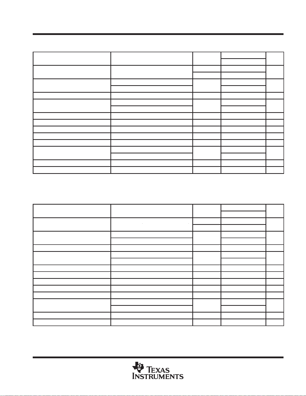
PARAMETER
TEST CONDITIONS
T
†
UNIT
Output voltage
O
,
I
,
V
Input voltage regulation
25°C
mV
Output voltage regulation
25°C
mV
Bias current change
0°C to 125°C
mA
PARAMETER
TEST CONDITIONS
T
†
UNIT
Output voltage
O
,
I
,
V
Input voltage regulation
25°C
mV
Output voltage regulation
25°C
mV
Bias current change
0°C to 125°C
mA
µA7800 SERIES
POSITIVE-VOLTAGE REGULATORS
SLVS056E – MAY 1976 – REVISED JULY 1999
electrical characteristics at specified virtual junction temperature, VI = 14 V, IO = 500 mA (unless
otherwise noted)
J
I
p
p
Ripple rejection VI = 11.5 V to 21.5 V, f = 120 Hz 0°C to 125°C 55 72 dB
p
Output resistance f = 1 kHz 0°C to 125°C 0.016 Ω
Temperature coefficient of output voltage IO = 5 mA 0°C to 125°C –0.8 mV/°C
Output noise voltage f = 10 Hz to 100 kHz 25°C 52 µV
Dropout voltage IO = 1 A 25°C 2 V
Bias current 25°C 4.3 8 mA
Short-circuit output current 25°C 450 mA
Peak output current 25°C 2.2 A
†
Pulse-testing techniques maintain the junction temperature as close to the ambient temperature as possible. Thermal effects must be taken into
account separately . All characteristics are measured with a 0.33-µF capacitor across the input and a 0.1-µF capacitor across the output.
= 5 mA to 1 A, V
PD ≤ 15 W
VI = 10.5 V to 25 V
VI = 11 V to 17 V
IO = 5 mA to 1.5 A
IO = 250 mA to 750 mA
VI = 10.5 V to 25 V
IO = 5 mA to 1 A
= 10.5 V to 23 V,
25°C 7.7 8 8.3
0°C to 125°C 7.6 8.4
°
°
°
°
µA7808C
MIN TYP MAX
6 160
2 80
12 160
4 80
1
0.5
electrical characteristics at specified virtual junction temperature, VI = 15 V, IO = 500 mA (unless
otherwise noted)
J
I
p
p
Ripple rejection VI = 11.5 V to 21.5 V, f = 120 Hz 0°C to 125°C 54 70 dB
p
Output resistance f = 1 kHz 0°C to 125°C 0.016 Ω
Temperature coefficient of output voltage IO = 5 mA 0°C to 125°C –0.8 mV/°C
Output noise voltage f = 10 Hz to 100 kHz 25°C 55 µV
Dropout voltage IO = 1 A 25°C 2 V
Bias current 25°C 4.3 8 mA
Short-circuit output current 25°C 450 mA
Peak output current 25°C 2.2 A
†
Pulse-testing techniques maintain the junction temperature as close to the ambient temperature as possible. Thermal effects must be taken into
account separately . All characteristics are measured with a 0.33-µF capacitor across the input and a 0.1-µF capacitor across the output.
= 5 mA to 1 A, V
PD ≤ 15 W
VI = 10.5 V to 25 V
VI = 11 V to 17 V
IO = 5 mA to 1.5 A
IO = 250 mA to 750 mA
VI = 10.5 V to 25 V
IO = 5 mA to 1 A
= 11 V to 23.5 V,
25°C 8.15 8.5 8.85
0°C to 125°C 8.1 8.9
°
°
°
°
µA7885C
MIN TYP MAX
6 170
2 85
12 170
4 85
1
0.5
POST OFFICE BOX 655303 • DALLAS, TEXAS 75265
5
Page 6
µA7800 SERIES
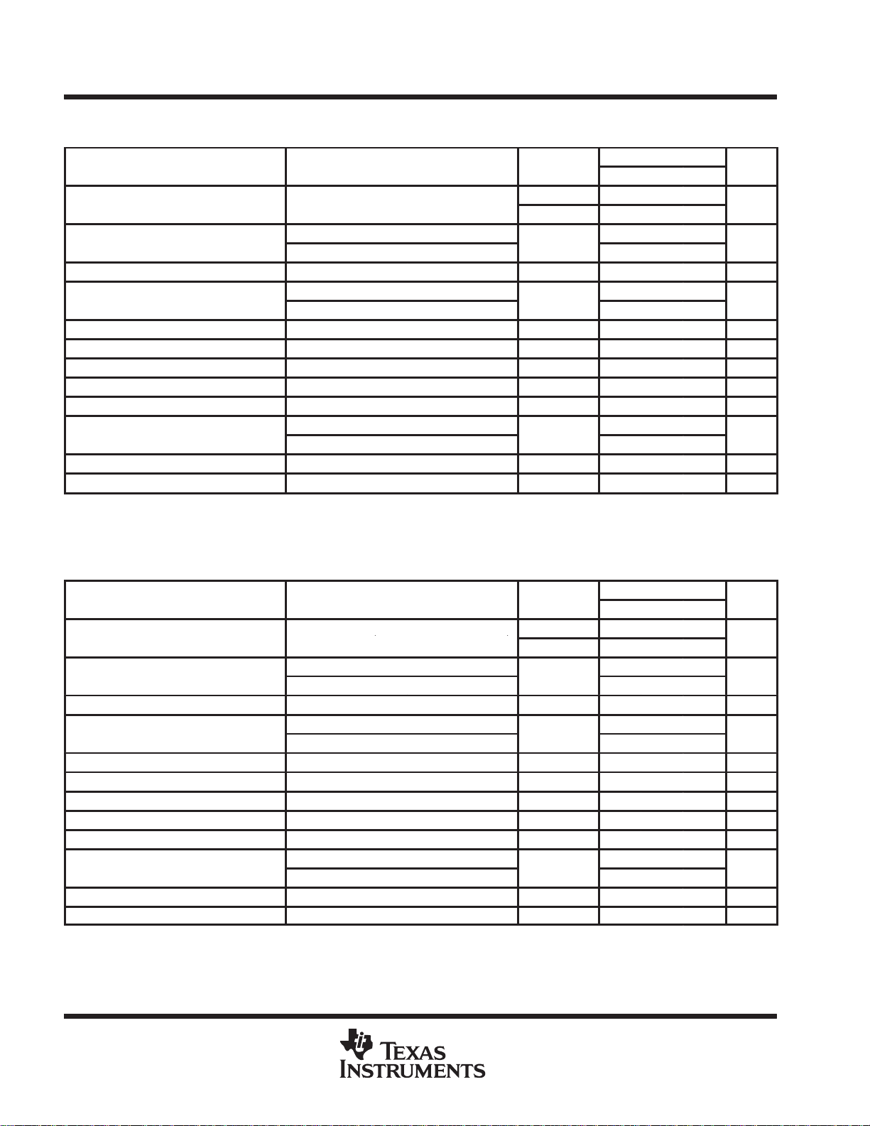
PARAMETER
TEST CONDITIONS
T
†
UNIT
Output voltage
O
,
I
,
V
Input voltage regulation
25°C
mV
Output voltage regulation
25°C
mV
Bias current change
0°C to 125°C
mA
PARAMETER
TEST CONDITIONS
T
†
UNIT
Output voltage
O
,
I
,
V
Input voltage regulation
25°C
mV
Output voltage regulation
25°C
mV
Bias current change
0°C
125°C
mA
POSITIVE-VOLTAGE REGULATORS
SLVS056E – MAY 1976 – REVISED JULY 1999
electrical characteristics at specified virtual junction temperature, VI = 17 V, IO = 500 mA (unless
otherwise noted)
J
I
p
p
Ripple rejection VI = 13 V to 23 V, f = 120 Hz 0°C to 125°C 55 71 dB
p
Output resistance f = 1 kHz 0°C to 125°C 0.018 W
Temperature coefficient of output voltage IO = 5 mA 0°C to 125°C –1 mV/°C
Output noise voltage f = 10 Hz to 100 kHz 25°C 70 µV
Dropout voltage IO = 1 A 25°C 2 V
Bias current 25°C 4.3 8 mA
Short-circuit output current 25°C 400 mA
Peak output current 25°C 2.2 A
†
Pulse-testing techniques maintain the junction temperature as close to the ambient temperature as possible. Thermal effects must be taken into
account separately . All characteristics are measured with a 0.33-µF capacitor across the input and a 0.1-µF capacitor across the output.
= 5 mA to 1 A, V
PD ≤ 15 W
VI = 12.5 V to 28 V
VI = 14 V to 20 V
IO = 5 mA to 1.5 A
IO = 250 mA to 750 mA
VI = 12.5 V to 28 V
IO = 5 mA to 1 A
= 12.5 V to 25 V,
25°C 9.6 10 10.4
0°C to 125°C 9.5 10 10.5
°
°
°
°
µA7810C
MIN TYP MAX
7 200
2 100
12 200
4 100
1
0.5
electrical characteristics at specified virtual junction temperature, VI = 19 V, IO = 500 mA (unless
otherwise noted)
J
I
p
p
Ripple rejection VI = 15 V to 25 V, f = 120 Hz 0°C to 125°C 55 71 dB
p
Output resistance f = 1 kHz 0°C to 125°C 0.018 W
Temperature coefficient of output voltage IO = 5 mA 0°C to 125°C –1 mV/°C
Output noise voltage f = 10 Hz to 100 kHz 25°C 75 µV
Dropout voltage IO = 1 A 25°C 2 V
Bias current 25°C 4.3 8 mA
Short-circuit output current 25°C 350 mA
Peak output current 25°C 2.2 A
†
Pulse-testing techniques maintain the junction temperature as close to the ambient temperature as possible. Thermal effects must be taken into
account separately . All characteristics are measured with a 0.33-µF capacitor across the input and a 0.1-µF capacitor across the output.
= 5 mA to 1 A, V
PD ≤ 15 W
VI = 14.5 V to 30 V
VI = 16 V to 22 V
IO = 5 mA to 1.5 A
IO = 250 mA to 750 mA
VI = 14.5 V to 30 V
IO = 5 mA to 1 A
= 14.5 V to 27 V,
25°C 11.5 12 12.5
0°C to 125°C 11.4 12.6
°
°
to
µA7812C
MIN TYP MAX
10 240
3 120
12 240
4 120
1
0.5
6
POST OFFICE BOX 655303 • DALLAS, TEXAS 75265
Page 7
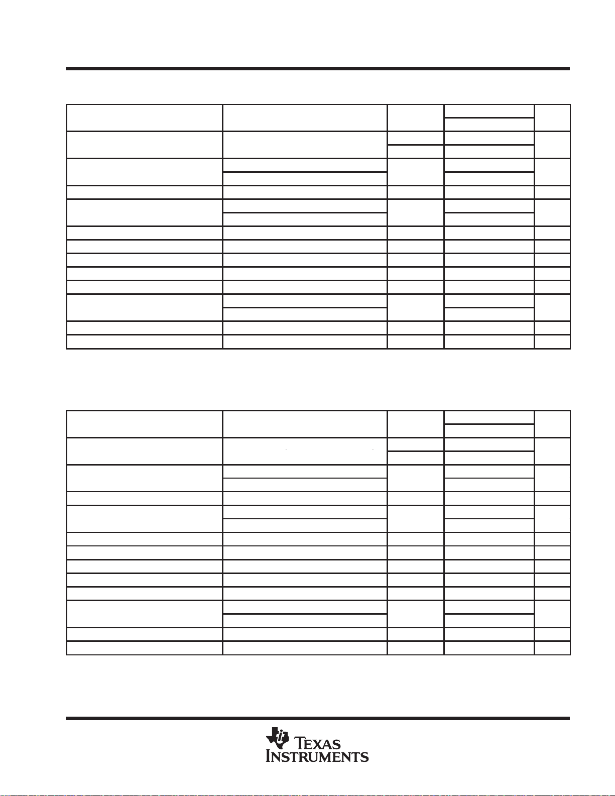
PARAMETER
TEST CONDITIONS
T
†
UNIT
Output voltage
O
,
I
,
V
Input voltage regulation
25°C
mV
Output voltage regulation
25°C
mV
Bias current change
0°C to 125°C
mA
PARAMETER
TEST CONDITIONS
T
†
UNIT
Output voltage
O
,
I
,
V
Input voltage regulation
25°C
mV
Output voltage regulation
25°C
mV
Bias current change
0°C to 125°C
mA
µA7800 SERIES
POSITIVE-VOLTAGE REGULATORS
SLVS056E – MAY 1976 – REVISED JULY 1999
electrical characteristics at specified virtual junction temperature, VI = 23 V, IO = 500 mA (unless
otherwise noted)
J
I
p
p
Ripple rejection VI = 18.5 V to 28.5 V, f = 120 Hz 0°C to 125°C 54 70 dB
p
Output resistance f = 1 kHz 0°C to 125°C 0.019 W
Temperature coefficient of output voltage IO = 5 mA 0°C to 125°C –1 mV/°C
Output noise voltage f = 10 Hz to 100 kHz 25°C 90 µV
Dropout voltage IO = 1 A 25°C 2 V
Bias current 25°C 4.4 8 mA
Short-circuit output current 25°C 230 mA
Peak output current 25°C 2.1 A
†
Pulse-testing techniques maintain the junction temperature as close to the ambient temperature as possible. Thermal effects must be taken into
account separately . All characteristics are measured with a 0.33-µF capacitor across the input and a 0.1-µF capacitor across the output.
= 5 mA to 1 A, V
PD ≤ 15 W
VI = 17.5 V to 30 V
VI = 20 V to 26 V
IO = 5 mA to 1.5 A
IO = 250 mA to 750 mA
VI = 17.5 V to 30 V
IO = 5 mA to 1 A
= 17.5 V to 30 V,
25°C 14.4 15 15.6
0°C to 125°C 14.25 15.75
°
°
°
°
µA7815C
MIN TYP MAX
11 300
3 150
12 300
4 150
1
0.5
electrical characteristics at specified virtual junction temperature, VI = 27 V, IO = 500 mA (unless
otherwise noted)
J
I
p
p
Ripple rejection VI = 22 V to 32 V, f = 120 Hz 0°C to 125°C 53 69 dB
p
Output resistance f = 1 kHz 0°C to 125°C 0.022 W
Temperature coefficient of output voltage IO = 5 mA 0°C to 125°C –1 mV/°C
Output noise voltage f = 10 Hz to 100 kHz 25°C 110 µV
Dropout voltage IO = 1 A 25°C 2 V
Bias current 25°C 4.5 8 mA
Short-circuit output current 25°C 200 mA
Peak output current 25°C 2.1 A
†
Pulse-testing techniques maintain the junction temperature as close to the ambient temperature as possible. Thermal effects must be taken into
account separately . All characteristics are measured with a 0.33-µF capacitor across the input and a 0.1-µF capacitor across the output.
= 5 mA to 1 A, V
PD ≤ 15 W
VI = 21 V to 33 V
VI = 24 V to 30 V
IO = 5 mA to 1.5 A
IO = 250 mA to 750 mA
VI = 21 V to 33 V
IO = 5 mA to 1 A
= 21 V to 33 V,
25°C 17.3 18 18.7
0°C to 125°C 17.1 18.9
°
°
°
°
µA7818C
MIN TYP MAX
15 360
5 180
12 360
4 180
1
0.5
POST OFFICE BOX 655303 • DALLAS, TEXAS 75265
7
Page 8
µA7800 SERIES
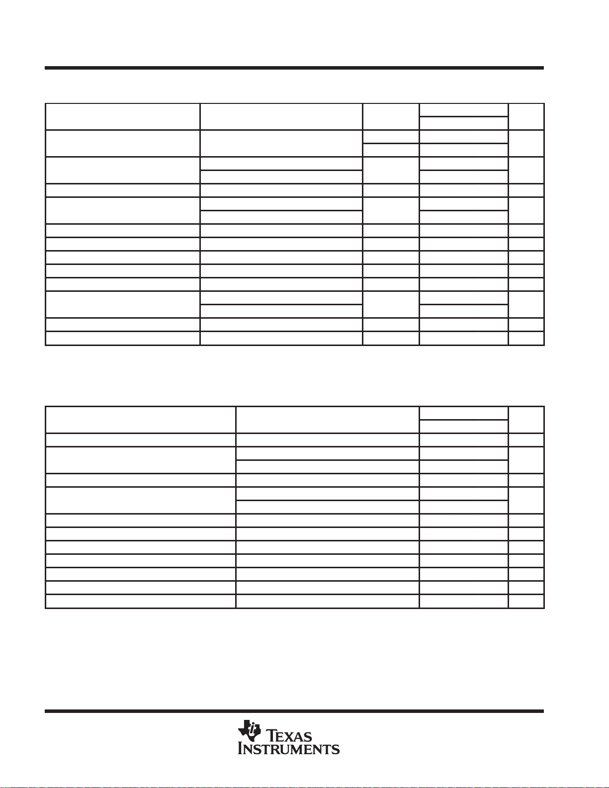
PARAMETER
TEST CONDITIONS
T
†
UNIT
Output voltage
O
,
I
,
V
Input voltage regulation
25°C
mV
Output voltage regulation
25°C
mV
Bias current change
0°C to 125°C
mA
PARAMETER
TEST CONDITIONS
UNIT
Input voltage regulation
mV
Output voltage regulation
mV
POSITIVE-VOLTAGE REGULATORS
SLVS056E – MAY 1976 – REVISED JULY 1999
electrical characteristics at specified virtual junction temperature, VI = 33 V, IO = 500 mA (unless
otherwise noted)
J
I
p
p
Ripple rejection VI = 28 V to 38 V, f = 120 Hz 0°C to 125°C 50 66 dB
p
Output resistance f = 1 kHz 0°C to 125°C 0.028 W
Temperature coefficient of output voltage IO = 5 mA 0°C to 125°C –1.5 mV/°C
Output noise voltage f = 10 Hz to 100 kHz 25°C 170 µV
Dropout voltage IO = 1 A 25°C 2 V
Bias current 25°C 4.6 8 mA
Short-circuit output current 25°C 150 mA
Peak output current 25°C 2.1 A
†
Pulse-testing techniques maintain the junction temperature as close to the ambient temperature as possible. Thermal effects must be taken into
account separately . All characteristics are measured with a 0.33-µF capacitor across the input and a 0.1-µF capacitor across the output.
= 5 mA to 1 A, V
PD ≤ 15 W
VI = 27 V to 38 V
VI = 30 V to 36 V
IO = 5 mA to 1.5 A
IO = 250 mA to 750 mA
VI = 27 V to 38 V
IO = 5 mA to 1 A
= 27 V to 38 V,
25°C 23 24 25
0°C to 125°C 22.8 25.2
°
°
°
°
µA7824C
MIN TYP MAX
18 480
6 240
12 480
4 240
1
0.5
electrical characteristics at specified virtual junction temperature, VI = 10 V , IO = 500 mA, TJ = 25°C
(unless otherwise noted)
Output voltage 5 V
p
Ripple rejection VI = 8 V to 18 V, f = 120 Hz 78 dB
p
Output resistance f = 1 kHz 0.017 W
Temperature coefficient of output voltage IO = 5 mA –1.1 mV/°C
Output noise voltage f = 10 Hz to 100 kHz 40 µV
Dropout voltage IO = 1 A 2 V
Bias current 4.2 mA
Short-circuit output current 750 mA
Peak output current 2.2 A
†
Pulse-testing techniques maintain the junction temperature as close to the ambient temperature as possible. Thermal effects must be taken into
account separately . All characteristics are measured with a 0.33-µF capacitor across the input and a 0.1-µF capacitor across the output.
†
µA7805Y
MIN TYP MAX
VI = 7 V to 25 V 3
VI = 8 V to 12 V 1
IO = 5 mA to 1.5 A 15
IO = 250 mA to 750 mA 5
8
POST OFFICE BOX 655303 • DALLAS, TEXAS 75265
Page 9
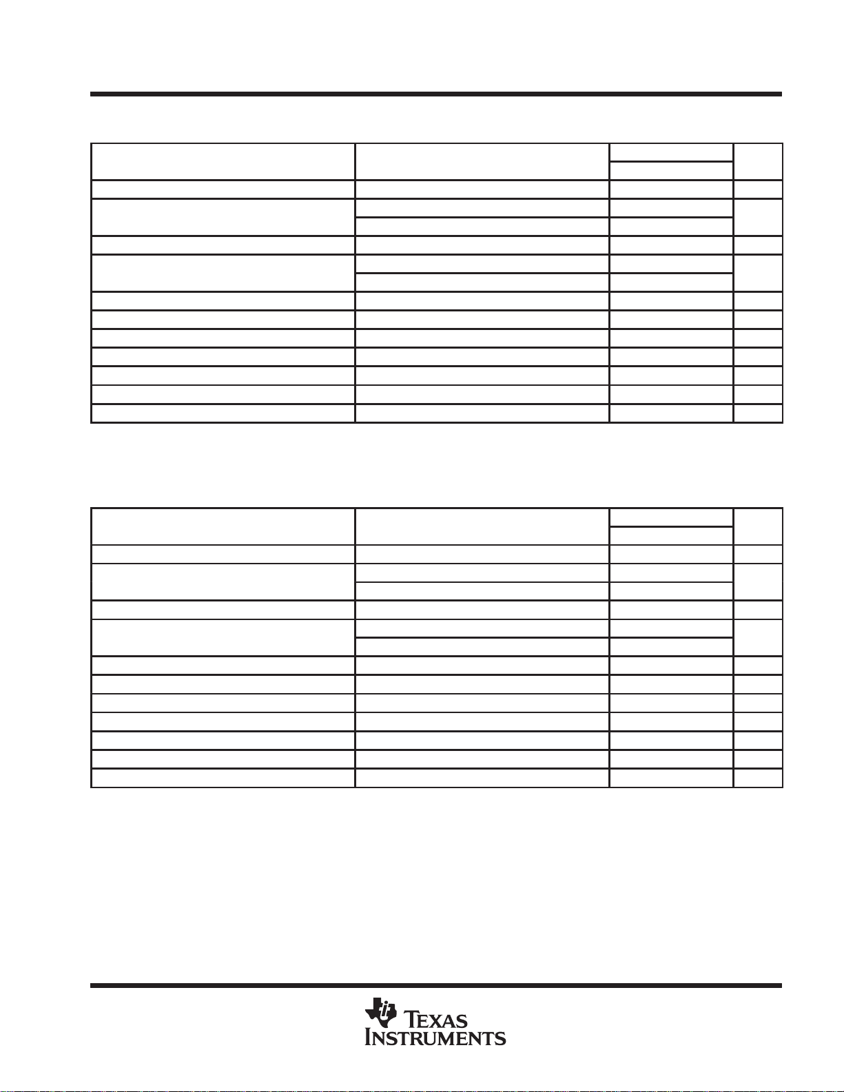
PARAMETER
TEST CONDITIONS
UNIT
Input voltage regulation
mV
Output voltage regulation
mV
PARAMETER
TEST CONDITIONS
UNIT
Input voltage regulation
mV
Output voltage regulation
mV
µA7800 SERIES
POSITIVE-VOLTAGE REGULATORS
SLVS056E – MAY 1976 – REVISED JULY 1999
electrical characteristics at specified virtual junction temperature, VI = 11 V, IO = 500 mA, TJ = 25°C
(unless otherwise noted)
Output voltage 6 V
p
Ripple rejection VI = 9 V to 19 V, f = 120 Hz 75 dB
p
Output resistance f = 1 kHz 0.019 W
Temperature coefficient of output voltage IO = 5 mA –0.8 mV/°C
Output noise voltage f = 10 Hz to 100 kHz 45 µV
Dropout voltage IO = 1 A 2 V
Bias current 4.3 mA
Short-circuit output current 550 mA
Peak output current 2.2 A
†
Pulse-testing techniques maintain the junction temperature as close to the ambient temperature as possible. Thermal effects must be taken into
account separately . All characteristics are measured with a 0.33-µF capacitor across the input and a 0.1-µF capacitor across the output.
†
µA7806Y
MIN TYP MAX
VI = 8 V to 25 V 5
VI = 9 V to 13 V 1.5
IO = 5 mA to 1.5 A 14
IO = 250 mA to 750 mA 4
electrical characteristics at specified virtual junction temperature, VI = 14 V , IO = 500 mA, TJ = 25°C
(unless otherwise noted)
Output voltage 8 V
p
Ripple rejection VI = 11.5 V to 21.5 V, f = 120 Hz 72 dB
p
Output resistance f = 1 kHz 0.016 W
Temperature coefficient of output voltage IO = 5 mA –0.8 mV/°C
Output noise voltage f = 10 Hz to 100 kHz 52 µV
Dropout voltage IO = 1 A 2 V
Bias current 4.3 mA
Short-circuit output current 450 mA
Peak output current 2.2 A
†
Pulse-testing techniques maintain the junction temperature as close to the ambient temperature as possible. Thermal effects must be taken into
account separately . All characteristics are measured with a 0.33-µF capacitor across the input and a 0.1-µF capacitor across the output.
†
µA7808Y
MIN TYP MAX
VI = 10.5 V to 25 V 6
VI = 11 V to 17 V 2
IO = 5 mA to 1.5 A 12
IO = 250 mA to 750 mA 4
POST OFFICE BOX 655303 • DALLAS, TEXAS 75265
9
Page 10
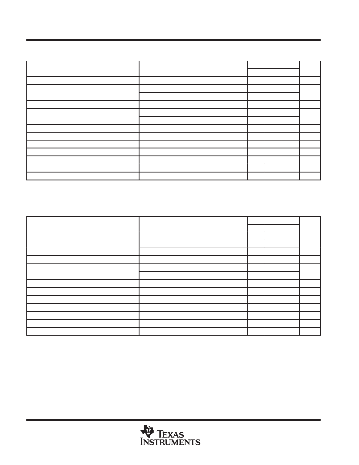
µA7800 SERIES
PARAMETER
TEST CONDITIONS
UNIT
Input voltage regulation
mV
Output voltage regulation
mV
PARAMETER
TEST CONDITIONS
UNIT
Input voltage regulation
mV
Output voltage regulation
mV
POSITIVE-VOLTAGE REGULATORS
SLVS056E – MAY 1976 – REVISED JULY 1999
electrical characteristics at specified virtual junction temperature, VI = 15 V , IO = 500 mA, TJ = 25°C
(unless otherwise noted)
Output voltage 8.5 V
p
Ripple rejection VI = 11.5 V to 21.5 V, f = 120 Hz 70 dB
p
Output resistance f = 1 kHz 0.016 W
Temperature coefficient of output voltage IO = 5 mA –0.8 mV/°C
Output noise voltage f = 10 Hz to 100 kHz 55 µV
Dropout voltage IO = 1 A 2 V
Bias current 4.3 mA
Short-circuit output current 450 mA
Peak output current 2.2 A
†
Pulse-testing techniques maintain the junction temperature as close to the ambient temperature as possible. Thermal effects must be taken into
account separately . All characteristics are measured with a 0.33-µF capacitor across the input and a 0.1-µF capacitor across the output.
†
µA7885Y
MIN TYP MAX
VI = 10.5 V to 25 V 6
VI = 11 V to 17 V 2
IO = 5 mA to 1.5 A 12
IO = 250 mA to 750 mA 4
electrical characteristics at specified virtual junction temperature, VI = 17 V , IO = 500 mA, TJ = 25°C
(unless otherwise noted)
Output voltage 10 V
p
Ripple rejection VI = 13 V to 23 V, f = 120 Hz 71 dB
p
Output resistance f = 1 kHz 0.018 W
Temperature coefficient of output voltage IO = 5 mA –1 mV/°C
Output noise voltage f = 10 Hz to 100 kHz 70 µV
Dropout voltage IO = 1 A 2 V
Bias current 4.3 mA
Short-circuit output current 400 mA
Peak output current 2.2 A
†
Pulse-testing techniques maintain the junction temperature as close to the ambient temperature as possible. Thermal effects must be taken into
account separately . All characteristics are measured with a 0.33-µF capacitor across the input and a 0.1-µF capacitor across the output.
†
µA7810Y
MIN TYP MAX
VI = 12.5 V to 28 V 7
VI = 14 V to 20 V 2
IO = 5 mA to 1.5 A 12
IO = 250 mA to 750 mA 4
10
POST OFFICE BOX 655303 • DALLAS, TEXAS 75265
Page 11
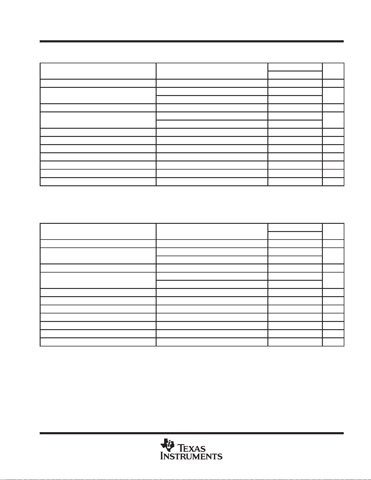
PARAMETER
TEST CONDITIONS
UNIT
Input voltage regulation
mV
Output voltage regulation
mV
PARAMETER
TEST CONDITIONS
UNIT
Input voltage regulation
mV
Output voltage regulation
mV
µA7800 SERIES
POSITIVE-VOLTAGE REGULATORS
SLVS056E – MAY 1976 – REVISED JULY 1999
electrical characteristics at specified virtual junction temperature, VI = 19 V , IO = 500 mA, TJ = 25°C
(unless otherwise noted)
Output voltage 12 V
p
Ripple rejection VI = 15 V to 25 V, f = 120 Hz 71 dB
p
Output resistance f = 1 kHz 0.018 W
Temperature coefficient of output voltage IO = 5 mA –1 mV/°C
Output noise voltage f = 10 Hz to 100 kHz 75 µV
Dropout voltage IO = 1 A 2 V
Bias current 4.3 mA
Short-circuit output current 350 mA
Peak output current 2.2 A
†
Pulse-testing techniques maintain the junction temperature as close to the ambient temperature as possible. Thermal effects must be taken into
account separately . All characteristics are measured with a 0.33-µF capacitor across the input and a 0.1-µF capacitor across the output.
†
µA7812Y
MIN TYP MAX
VI = 14.5 V to 30 V 10
VI = 16 V to 22 V 3
IO = 5 mA to 1.5 A 12
IO = 250 mA to 750 mA 4
electrical characteristics at specified virtual junction temperature, VI = 23 V , IO = 500 mA, TJ = 25°C
(unless otherwise noted)
Output voltage 15 V
p
Ripple rejection VI = 18.5 V to 28.5 V, f = 120 Hz 70 dB
p
Output resistance f = 1 kHz 0.019 W
Temperature coefficient of output voltage IO = 5 mA –1 mV/°C
Output noise voltage f = 10 Hz to 100 kHz 90 µV
Dropout voltage IO = 1 A 2 V
Bias current 4.4 mA
Short-circuit output current 230 mA
Peak output current 2.1 A
†
Pulse-testing techniques maintain the junction temperature as close to the ambient temperature as possible. Thermal effects must be taken into
account separately . All characteristics are measured with a 0.33-µF capacitor across the input and a 0.1-µF capacitor across the output.
†
µA7815Y
MIN TYP MAX
VI = 17.5 V to 30 V 11
VI = 20 V to 26 V 3
IO = 5 mA to 1.5 A 12
IO = 250 mA to 750 mA 4
POST OFFICE BOX 655303 • DALLAS, TEXAS 75265
11
Page 12
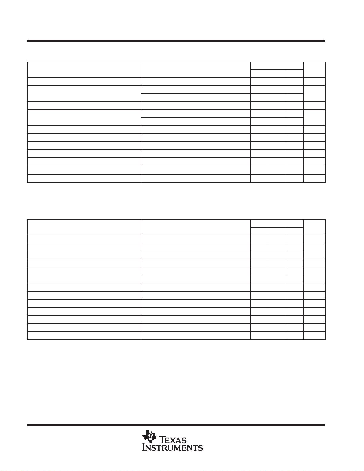
µA7800 SERIES
PARAMETER
TEST CONDITIONS
UNIT
Input voltage regulation
mV
Output voltage regulation
mV
PARAMETER
TEST CONDITIONS
UNIT
Input voltage regulation
mV
Output voltage regulation
mV
POSITIVE-VOLTAGE REGULATORS
SLVS056E – MAY 1976 – REVISED JULY 1999
electrical characteristics at specified virtual junction temperature, VI = 27 V , IO = 500 mA, TJ = 25°C
(unless otherwise noted)
Output voltage 18 V
p
Ripple rejection VI = 22 V to 32 V, f = 120 Hz 69 dB
p
Output resistance f = 1 kHz 0.022 W
Temperature coefficient of output voltage IO = 5 mA –1 mV/°C
Output noise voltage f = 10 Hz to 100 kHz 110 µV
Dropout voltage IO = 1 A 2 V
Bias current 4.5 mA
Short-circuit output current 200 mA
Peak output current 2.1 A
†
Pulse-testing techniques maintain the junction temperature as close to the ambient temperature as possible. Thermal effects must be taken into
account separately . All characteristics are measured with a 0.33-µF capacitor across the input and a 0.1-µF capacitor across the output.
†
µA7818Y
MIN TYP MAX
VI = 21 V to 33 V 15
VI = 24 V to 30 V 5
IO = 5 mA to 1.5 A 12
IO = 250 mA to 750 mA 4
electrical characteristics at specified virtual junction temperature, VI = 33 V , IO = 500 mA, TJ = 25°C
(unless otherwise noted)
Output voltage 24 V
p
Ripple rejection VI = 28 V to 38 V, f = 120 Hz 66 dB
p
Output resistance f = 1 kHz 0.028 W
Temperature coefficient of output voltage IO = 5 mA –1.5 mV/°C
Output noise voltage f = 10 Hz to 100 kHz 170 µV
Dropout voltage IO = 1 A 2 V
Bias current 4.6 mA
Short-circuit output current 150 mA
Peak output current 2.1 A
†
Pulse-testing techniques maintain the junction temperature as close to the ambient temperature as possible. Thermal effects must be taken into
account separately . All characteristics are measured with a 0.33-µF capacitor across the input and a 0.1-µF capacitor across the output.
†
µA7824Y
MIN TYP MAX
VI = 27 V to 38 V 18
VI = 30 V to 36 V 6
IO = 5 mA to 1.5 A 12
IO = 250 mA to 750 mA 4
12
POST OFFICE BOX 655303 • DALLAS, TEXAS 75265
Page 13
µA7800 SERIES
POSITIVE-VOLTAGE REGULATORS
SLVS056E – MAY 1976 – REVISED JULY 1999
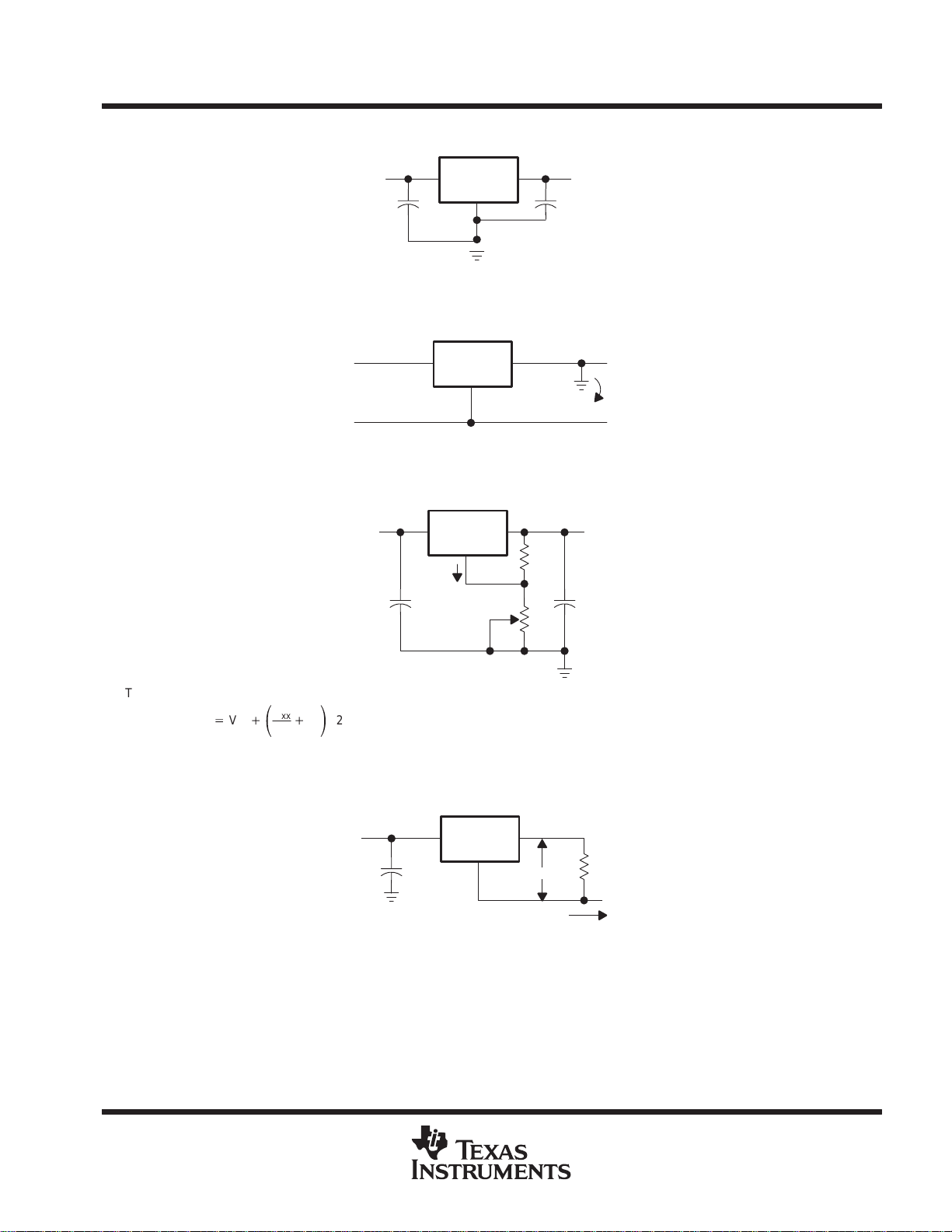
APPLICATION INFORMATION
+V
µA78xx
+V
O
0.1 µF0.33 µF
Figure 1. Fixed-Output Regulator
COM
OUTIN
G
I
L
–V
O
+
V
I
–
µA78xx
Figure 2. Positive Regulator in Negative Configuration (VI Must Float)
Input Output
µA78xx
I
O
0.33 µF
R1
0.1 µF
R2
NOTE A: The following formula is used when Vxx is the nominal output voltage (output to common) of the fixed regulator:
V
xx
Vxx)
ǒ
V
+
O
R1
)
Ǔ
I
R2
Q
Figure 3. Adjustable-Output Regulator
Input
0.33 µF
IO = (VO/R1) + IO Bias Current
µA78xx
V
O(Reg)
R1
Output
I
O
Figure 4. Current Regulator
POST OFFICE BOX 655303 • DALLAS, TEXAS 75265
13
Page 14
µA7800 SERIES
POSITIVE-VOLTAGE REGULATORS
SLVS056E – MAY 1976 – REVISED JULY 1999
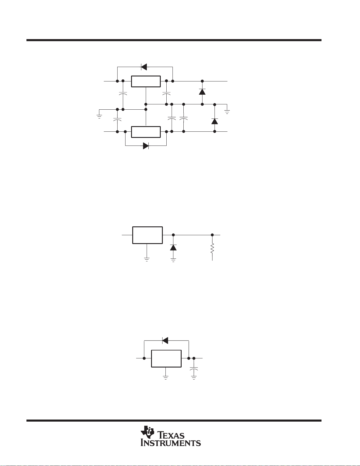
APPLICATION INFORMATION
1N4001
20-V Input
0.33 µF
–20-V Input
2 µF
µA7815C
µA7915C
1N4001
1 µF
0.1 µF
0.1 µF
VO = 15 V
1N4001
1N4001
VO = –15 V
Figure 5. Regulated Dual Supply
operation with a load common to a voltage of opposite polarity
In many cases, a regulator powers a load that is not connected to ground but, instead, is connected to a voltage
source of opposite polarity (e.g., operational amplifiers, level-shifting circuits, etc.). In these cases, a clamp
diode should be connected to the regulator output as shown in Figure 6. This protects the regulator from output
polarity reversals during startup and short-circuit operation.
+V
I
µA78xx
1N4001
or
Equivalent
+V
O
–V
O
Figure 6. Output Polarity-Reversal-Protection Circuit
reverse-bias protection
Occasionally , the input voltage to the regulator can collapse faster than the output voltage. This can occur, for
example, when the input supply is crowbarred during an output overvoltage condition. If the output voltage is
greater than approximately 7 V , the emitter-base junction of the series-pass element (internal or external) could
break down and be damaged. To prevent this, a diode shunt can be used as shown in Figure 7.
V
I
µA78xx
Figure 7. Reverse-Bias-Protection Circuit
+V
O
14
POST OFFICE BOX 655303 • DALLAS, TEXAS 75265
Page 15

IMPORTANT NOTICE
T exas Instruments and its subsidiaries (TI) reserve the right to make changes to their products or to discontinue
any product or service without notice, and advise customers to obtain the latest version of relevant information
to verify, before placing orders, that information being relied on is current and complete. All products are sold
subject to the terms and conditions of sale supplied at the time of order acknowledgement, including those
pertaining to warranty, patent infringement, and limitation of liability.
TI warrants performance of its semiconductor products to the specifications applicable at the time of sale in
accordance with TI’s standard warranty. Testing and other quality control techniques are utilized to the extent
TI deems necessary to support this warranty . Specific testing of all parameters of each device is not necessarily
performed, except those mandated by government requirements.
CERTAIN APPLICA TIONS USING SEMICONDUCT OR PRODUCTS MAY INVOLVE POTENTIAL RISKS OF
DEATH, PERSONAL INJURY, OR SEVERE PROPERTY OR ENVIRONMENTAL DAMAGE (“CRITICAL
APPLICATIONS”). TI SEMICONDUCTOR PRODUCTS ARE NOT DESIGNED, AUTHORIZED, OR
WARRANTED TO BE SUITABLE FOR USE IN LIFE-SUPPORT DEVICES OR SYSTEMS OR OTHER
CRITICAL APPLICA TIONS. INCLUSION OF TI PRODUCTS IN SUCH APPLICATIONS IS UNDERST OOD TO
BE FULLY AT THE CUSTOMER’S RISK.
In order to minimize risks associated with the customer’s applications, adequate design and operating
safeguards must be provided by the customer to minimize inherent or procedural hazards.
TI assumes no liability for applications assistance or customer product design. TI does not warrant or represent
that any license, either express or implied, is granted under any patent right, copyright, mask work right, or other
intellectual property right of TI covering or relating to any combination, machine, or process in which such
semiconductor products or services might be or are used. TI’s publication of information regarding any third
party’s products or services does not constitute TI’s approval, warranty or endorsement thereof.
Copyright 1999, Texas Instruments Incorporated
 Loading...