

Page 1
Plastic-Encapsulate Mosfets
FEATURES
High density cell design for low RDS(ON)
Voltage controlled small signal switch.
Rugged and reliable.
High saturation current capability.
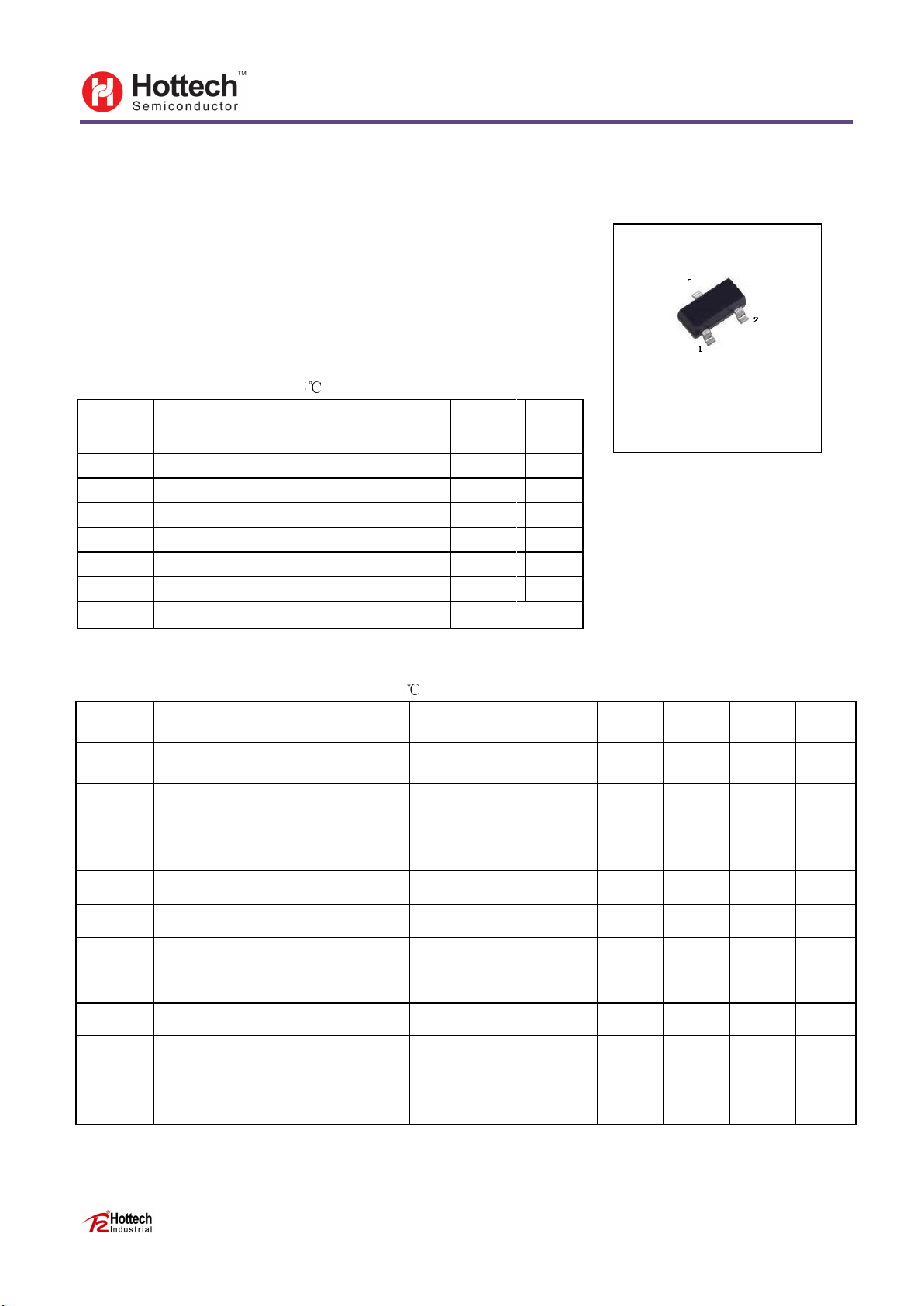
MAXIMUM RATINGS (TA=25 unless otherwise noted)
Symbol
V
DS
V
DGR
V
GS
I
D
I
DM
P
TOT
Rthj- amb Thermal resistance junction-ambient max
TJ, Tstg
Drain-source voltage (VGS= 0)
Drain-gate voltage (RGS= 20 kΩ)
Gate- sourcevoltage
Drain current (continuous) at TC= 25°C
(1)
Drain current (pulsed)
Total dissipation at TC= 25°C
Operating junction temperature, Storage temperature
Parameter
Ratings
60
60
±20
0.20
800
0.35
(2)
357.1
- 55 to 150 °C
Unit
V
V
V
A
mA
W
°C/W
2N7002
1.Gate
2.Source
3.Drain
SOT-23
ELECTRICAL CHARACTERISTICS (Tamb=25 unless otherwise specified)
Symbol Parameter Test conditions Min. Typ. Max. Unit
V
(BR)DSS
I
DSS
I
GSS
V
GS(th)
R
DS(on)
(3)
g
fs
C
iss
C
oss
C
rss
Drain-source breakdown voltage
Zero gate voltage
drain current (VDS= 0)
Gate-body leakage current (VDS= 0)
Gate threshold voltage
Static drain-source on resistance
Forward transconductance
Input capacitance Output capacitance
Reverse transfer
capacitance
ID= 250µA, VGS=0
VDS= max rating
VDS= max rating,
TC=125°C
VGS= ± 18V
VDS= VGS, ID= 250µA
VGS= 10V, ID= 0.5A
VGS= 4.5V, ID= 0.5A
VDS= 10V,ID= 0.5A
VDS= 25V, f = 1MHz,
VGS= 0
60 V
1
10
±100 nA
1 2.1 2.5 V
1.8
2
5
5.3
0.6 S
43
20
6
µA
µA
Ω
Ω
pF
pF
pF
GUANGDONG HOTTECH INDUSTRIAL CO,. LTD.
Page:P4-P1
Page 2
Page:P4-P2
Plastic-Encapsulate Mosfets
GUANGDONG HOTTECH INDUSTRIAL CO,. LTD.
2N7002
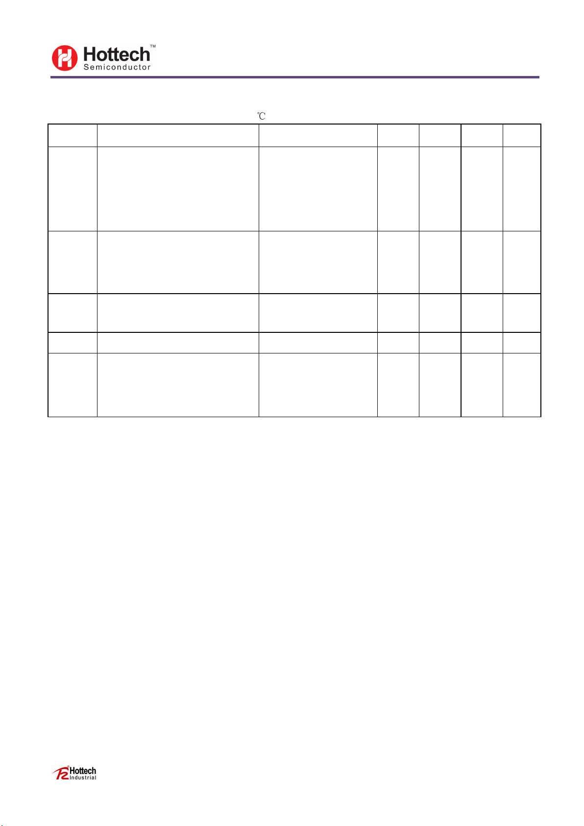
ELECTRICAL CHARACTERISTICS (Tamb=25 unless otherwise specified)
Symbol
Parameter
Test conditions
Min.
Typ.
Max.
Unit
t
d(on)
t
r
t
d(off)
t
f
Turn-on delay time
Rise time
Turn-off delay time
Fall time
V= 30V, I = 0.5A
RG= 4.7ΩVGS= 4.5V
5
15
7
8
ns
ns
ns
ns
Q
g
Q
gs
Q
gd
Total gate charge Gate-source charge
Gate-drain charge
VDD= 30V, ID= 1A,
VGS= 5V
1.4
0.8
0.5
2nCnC
nC
I
SD
I
SDM
(4)
Source-drain current Source-drain
current (pulsed)
0.35
1.40
A
A
V
SD
(5)
Forward on voltage
ISD= 1A, VGS= 0
1.2
V
t
rrQrr
I
RRM
Reverse recovery time Reverse recovery
charge Reverse recovery current
ISD= 1A, di/dt = 100A/µs,
VDD= 20V, Tj= 150°C
32
25
1.6
ns
nC
A
NOTE: 1. Pulse width limited by safe operating area 2. When mounted on 1inch2 FR-4, 2 Oz copper board.
3.Pulsed: Pulse duration = 300 µs, duty cycle 1.5 %. 4.Pulse width limited by safe operating area.
5.Pulsed: Pulse duration = 300 µs, duty cycle 1.5 %
Page 3
Plastic-Encapsulate Mosfets
2N7002
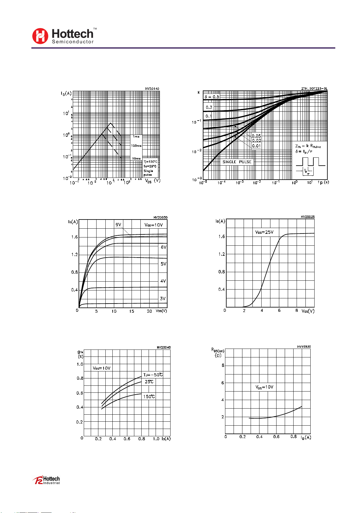
Typical Characteristics
Figure 1.Safe operating area Figure 2.Thermal impedance
Figure 3.Output characterisics Figure 4.Transfer characteristics
Figure 5.Transconductance Figure 6.Static drain-source on resistance
GUANGDONG HOTTECH INDUSTRIAL CO,. LTD.
Page:P4-P3
Page 4
Plastic-Encapsulate Mosfets
2N7002
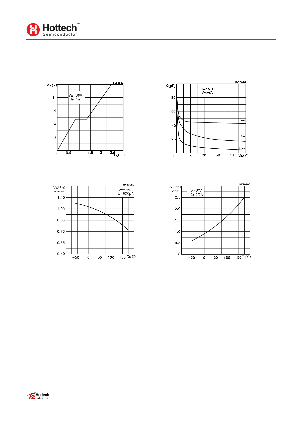
Typical Characteristics
Figure 7.Gate charge vs gate-source voltage Figure 8.Capacitance variations
Figure 9.Normalized gate threshold voltage
vs temperature
GUANGDONG HOTTECH INDUSTRIAL CO,. LTD.
Figure 10.Normalized on resistance vs
temperature
Page:P4-P4
 Loading...