

Page 1

4-33, Kitakyuhoji 1-chome,
Yao-City, Osaka, 581-0071, Japan
User Guide for
CFU0321 RF Module
Specification for the CFU0321
Smart Energy RF module based on the
IEEE 802.15.4 and ZigBee specifications
Draft v.0.1
2011-4-24
Page 2

4-33, Kitakyuhoji 1-chome,
Yao-City, Osaka, 581-0071, Japan
Table of Contents
CFU0321 RF Module Description
The CFU0321 is a general purpose IEEE 802.15.4 RF module
designed with Smart Energy applications in mind. It features the
TI CC2520 RF transceiver, TI CC2591 2.4GHz Power Amplifier, I
MSP 430F5437 microcontroller with 256K of flash RAM and 16K of
RAM, 1MB external flash RAM, and pattern antenna. Depending on
the SKU, the following options are available:
• Board to Board connector
• Side through hole for surface mounted
The CFU0321 is designed to be surface mounted; however, board
to board connector is standard feature and allows Board to Board
connector to be attached for easy socketing.
The unit requires 2.7V – 3.6V unregulated DC supply; internal
voltage regulation supplies the radio. The nominal transmission
and reception distance is 100 meters with the on-board pattern
antenna.
TI Z-Stack 2.4 port is available for the CFU0321, along with an
implementation of the Smart Energy profile device(s). Also, the
TIMAC only firmware is available. Standard development
environment requires the MSP430 version of the IAR IDE toolset.
Programming the CFU0321 requires the HVE0704, the
development board specifically designed for the CFU0321.
Additionally a JTAG programmer is required.
Applications
The CFU0321 allows devices to join the ZigBee SE 1.x network
currently being deployed by the utility companies. The following
Page 3
4-33, Kitakyuhoji 1-chome,
Yao-City, Osaka, 581-0071, Japan
are some applications of the CFU0321 RF module.
Energy Service Portal Utility Meters
Gateway Devices Home Automation Devices
Load Control Devices Telecom Applications
In-home Displays Health care products
Reference firmware implementations are available for various
devices. For details, please contact Wireless Glue Networks, Inc.
CFU0321 Key Features
The CFU0321 is a general purpose IEEE 802.15.4 RF module
based on the TI CC2520, CC2591 and MSP430. The module also
includes a serial 1MB Flash RAM as standard.
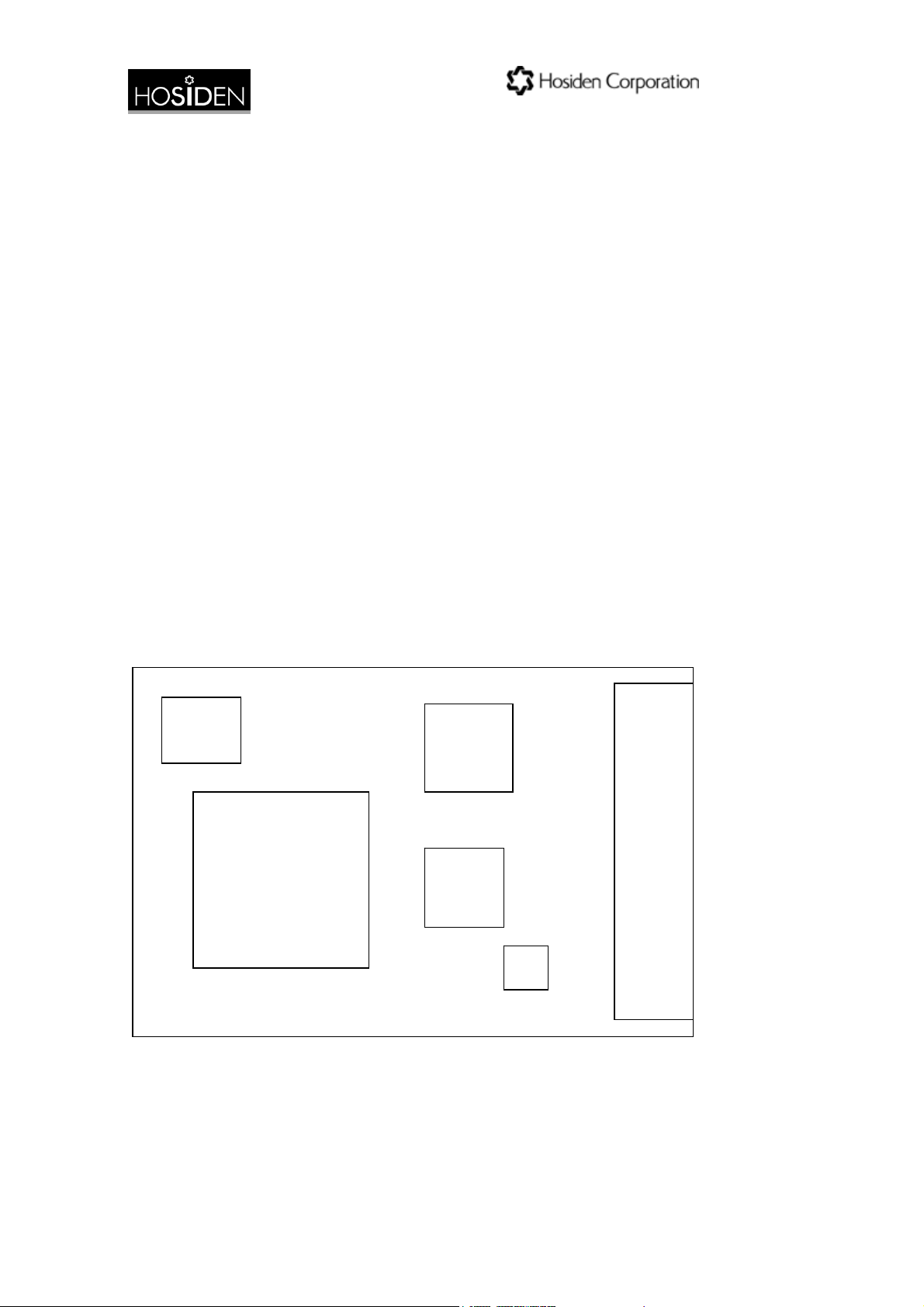
Module Overview
Serial
Flash
RAM
MSP430F5437
CC2520
RF
CC2591
PA
Pattern Antenna
RF Connector
With Switch
The CFU0321 is an IEEE 802.15.4 RF module optimized for the
Smart Energy 1.x feature set requirements from the ZigBee
Alliance. The module provides turnkey implementation of the
ZigBee 2007 platform based on the Z-Stack 2.4x, and ZigBee
Page 4

4-33, Kitakyuhoji 1-chome,
Yao-City, Osaka, 581-0071, Japan
Cluster Library, along with the required device firmware (e.g.
In-home Display, etc.). The CFU0321 has been tested with the
Smart Energy Device Simulator, the validated test harness
solution for the ZigBee Alliance for Smart Energy 1.0 Application
Profile, and therefore assured of interoperability with all major
devices supporting Smart Energy application profiles.
Specifications
Development Board Schematic Layout Information
The best way to incorporate CFU0321 into devices is to implement
the electrical connections as described on the HVE0704
development board. The schematic for the development board is
given below.
Operating conditions
Page 5
4-33, Kitakyuhoji 1-chome,
Yao-City, Osaka, 581-0071, Japan
Parameter Min Max Unit
Operating Voltage 2.7 3.6 V
Operating Temperature -20 60
℃
Electrical Characteristics
Parameter Condition Typ Unit
Transmission Current TXPOWER = 0xF9 140 mA
Receive Current HGM = 1 35 mA
TXPOWER = 0xF9 17 dBm
Transmit Power
TXPOWER = 0x2C 10 dBm
Receive Sensitivity HGM = 1 -96 dBm
Mounting Information
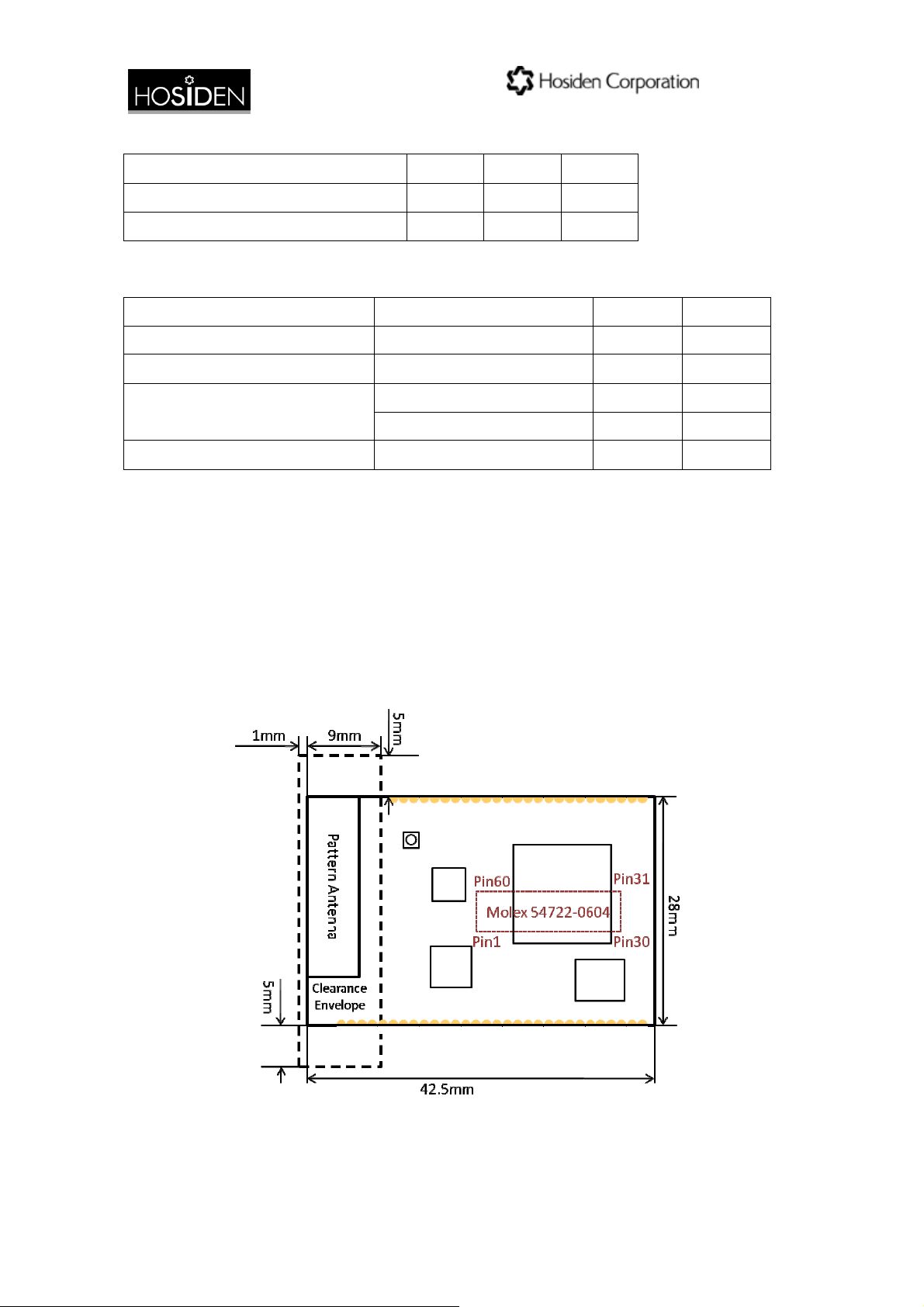
The following diagram serves as guidance in incorporating the
CFU0321 module onto other circuit boards. The following is for
Board-to-Board connector equipped version of the module.
It is important to note that the ground plane should be absent
directly beneath the pattern antenna.
Page 6
4-33, Kitakyuhoji 1-chome,
Yao-City, Osaka, 581-0071, Japan
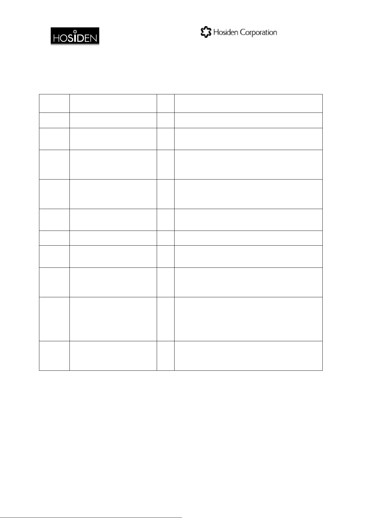
Pin Assignment and Layout
CFU0321 Pin Assignments
PIN ID Function I/O Description
1 GND1
2
3
4
5
6 P2.5/ROSC I/O General-purpose digital I/O with port interrupt
7
8
P2.0/TA1CLK/MCLK I/O
P2.1/TA1.0 I/O
P2.3/TA1.2 I/O
P2.4/RTCCLK I/O
P2.6/ACLK I/O
P2.7/ADC12CLK/DMAE0 I/O
General-purpose digital I/O with port interrupt
TA1 clock signal TA1CLK input MCLK output
General-purpose digital I/O with port interrupt
TA1 CCR0 capture: CCI0A input, compare: Out0
output
General-purpose digital I/O with port interrupt
TA1 CCR1 capture: CCI1A input, compare: Out1
output
General-purpose digital I/O with port interrupt
RTCCLK output
General-purpose digital I/O with port interrupt
ACLK output (divided by 1, 2, 4, 8, 16, or 32)
General-purpose digital I/O with port interrupt
Conversion clock input ADC DMA external
trigger input
9
10
General-purpose digital I/O
Slave transmit enable – USCI_B0 SPI mode
P3.0/UCB0STE/UCA0CLK I/O
P3.1/UCB0SIMO/
UCB0SDA/[FLASH_SIMO]
P3.0/UCB0STE/UCA0CLK 33 35 L5 I/O Clock
signal input – USCI_A0 SPI slave mode Clock
signal output – USCI_A0 SPI master mode
General-purpose digital I/O
I/O
Slave in, master out – USCI_B0 SPI mode I2C
data – USCI_B0 I2C mode
Page 7
4-33, Kitakyuhoji 1-chome,
Yao-City, Osaka, 581-0071, Japan
PIN ID Function I/O Description
11
12
13
14
15
P3.2/UCB0SOMI/
UCB0SCL/[FLASH_SOMI]
P3.3/UCB0CLK/UCA0STE/
[FLASH_CLK]
P3.4/UCA0TXD/
UCA0SIMO
P3.5/UCA0RXD/
UCA0SOMI
P3.6/UCB1STE/UCA1CLK4
120
General-purpose digital I/O
P3.2/UCB0SOMI/UCB0SCL 35 37 J6 I/O Slave
I/O
out, master in – USCI_B0 SPI mode I2C clock –
USCI_B0 I2C mode
General-purpose digital I/O
Clock signal input – USCI_B0 SPI slave mode
P3.3/UCB0CLK/UCA0STE 36 38 L6 I/O Clock
I/O
signal output – USCI_B0 SPI master modeSlave
transmit enable – USCI_A0 SPI mode
General-purpose digital I/O
P3.4/UCA0TXD/UCA0SIMO 39 39 L7 I/O
I/O
Transmit data – USCI_A0 UART mode Slave in,
master out – USCI_A0 SPI mode
General-purpose digital I/O
P3.5/UCA0RXD/UCA0SOMI 40 40 J7 I/O Receive
I/O
data – USCI_A0 UART mode Slave out, master
in – USCI_A0 SPI mode
General-purpose digital I/O
Slave transmit enable – USCI_B1 SPI mode
P3.6/UCB1STE/UCA1CLK 41 41 M8 I/O Clock
I/O
signal input – USCI_A1 SPI slave mode Clock
signal output – USCI_A1 SPI master mode
16
17
18
19
20
General-purpose digital I/O
P4.0/TB0.0 I/O
P4.1/TB0.1 I/O
P4.2/TB0.2 I/O
P4.3/TB0.3 I/O
P4.4/TB0.4 I/O
TB0 capture CCR0: CCI0A/CCI0B input,
compare:Out0 output
General-purpose digital I/O
TB0 capture CCR1: CCI1A/CCI1B input,
compare:Out1 output
General-purpose digital I/O
TB0 capture CCR2: CCI2A/CCI2B input,
compare:Out2 output
General-purpose digital I/O
TB0 capture CCR3: CCI3A/CCI3B input,
compare:Out3 output
General-purpose digital I/O
TB0 capture CCR4: CCI4A/CCI4B input,
compare:Out4 output
Page 8
4-33, Kitakyuhoji 1-chome,
Yao-City, Osaka, 581-0071, Japan
PIN ID Function I/O Description
21
P4.5/TB0.5 I/O
22
23
24
25
26 P4.7/TB0CLK/SMCLK I/O
27
P4.6/TB0.6 I/O
P5.0/VRE+/VeREF+ I/O
P5.1/VREF-/VeREF- I/O
P5.3/XT2OUT I/O
P5.6/UCA1TXD/UCA1SIM
O
I/O
General-purpose digital I/O
TB0 capture CCR4: CCI4A/CCI4B input,
compare:Out4 output
General-purpose digital I/O
B0 capture CCR6: CCI6A/CCI6B input,
compare:Out6 output
General-purpose digital I/O
P5.0/VREF+/VeREF+ 9 9 D1 I/O Output of
reference voltage to the ADC Input for an
external reference voltage to the ADC
General-purpose digital I/O
Negative terminal for the ADC's reference voltage
for both sources, thinternal reference voltage, or
an external applied reference voltage
General-purpose digital I/O
Output terminal of crystal oscillator XT2
General-purpose digital I/O
TB0 clock input SMCLK output
General-purpose digital I/O
P5.6/UCA1TXD/UCA1SIMO 53 56 K11 I/O
Transmit data – USCI_A1 UART mode Slave in,
master out – USCI_A1 SPI mode
28
29
30
31
General-purpose digital I/O
P7.3/TA1.2 I/O
P8.0/TA0.0 I/O
GND2
P8.1/TA0.1 I/O
TA1 CCR2 capture: CCI2B input, compare: Out2
output
General-purpose digital I/O
TA0 CCR0 capture: CCI0B input, compare: Out0
output
General-purpose digital I/O TA0 CCR1 capture:
CCI1B input, compare: Out1 output
Page 9
4-33, Kitakyuhoji 1-chome,
Yao-City, Osaka, 581-0071, Japan
PIN ID Function I/O Description
32
33
34 P8.4/TA0.4 I/O
35
36
37
38
P8.2/TA0.2 I/O
P8.3/TA0.3 I/O
P8.5/TA1.0 I/O
P8.6/TA1.1 I/O
TEST/SBWTCK I
PJ.0/TD0 I/O
General-purpose digital I/O TA0 CCR2 capture:
CCI2B input, compare: Out2 output
General-purpose digital I/O TA0 CCR3 capture:
CCI3B input, compare: Out3 output
General-purpose digital I/O TA0 CCR4 capture:
CCI4B input, compare: Out4 output
General-purpose digital I/O TA1 CCR0 capture:
CCI0B input, compare: Out0 output
General-purpose digital I/O P8.6/TA1.1 66 66 E11
I/O TA1 CCR1 capture: CCI1B input, compare:
Out1 output
Test m od e p in – select digital I/O on JTAG pins
Spy-bi-wire input clock
General-purpose digital I/O
Test data output port
39 PJ.1/TDI/TCLK I/O
40
41
42
43
44 P6.1/A1 I/O
45
PJ.2/TMS I/O
PJ.3/TCK I/O
/RESET/NMI/SBWTDIO I/O
P6.0/A0 I/O
P6.2/A2 I/O
General-purpose digital I/O
Test data input or test clock input
General-purpose digital I/O
Test mode select
General-purpose digital I/O
Test c lo ck
Reset input active low
RST/NMI/SBWTDIO9676A3I/ONon-maskable
interrupt input Spy-bi-wire data input/output
General-purpose digital I/O
Analog input A0 – ADC
General-purpose digital I/O
Analog input A1 – ADC
General-purpose digital I/O
Analog input A2 – ADC
Page 10
4-33, Kitakyuhoji 1-chome,
Yao-City, Osaka, 581-0071, Japan
PIN ID Function I/O Description
46
47
48 P6.5/A5 I/O
49
50
51
52
P6.3/A3 I/O
P6.4/A4 I/O
P6.6/A6 I/O
P6.7/A7 I/O
P7.4/A12 I/O
P7.5/A13 I/O
General-purpose digital I/O
Analog input A3 – ADC
General-purpose digital I/O
Analog input A4 – ADC
General-purpose digital I/O
Analog input A5 – ADC
General-purpose digital I/O
Analog input A6 – ADC
General-purpose digital I/O
Analog input A7 – ADC
General-purpose digital I/O
Analog input A12 –ADC
General-purpose digital I/O
Analog input A13 – ADC
53
54
55
P7.6/A14 I/O
P1.4/TA0.3 I/O
VCC +3.3V Input power supply
General-purpose digital I/O
Analog input A14 – ADC
General-purpose digital I/O with port interrupt
TA0 CCR3 capture: CCI3A input compare: Out3
output
Page 11
4-33, Kitakyuhoji 1-chome,
Yao-City, Osaka, 581-0071, Japan
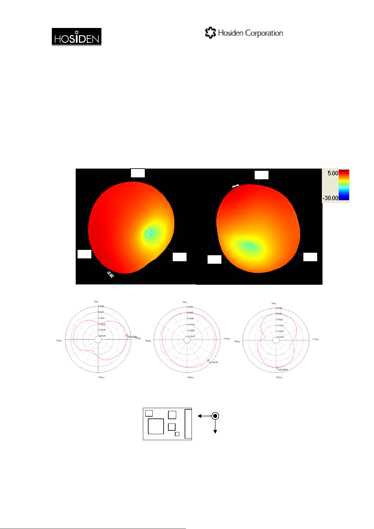
Antenna Gain Pattern
The CFU0321 comes with an onboard pattern antenna. The
diagram below shows the antenna gain pattern of the pattern
antenna.
Note: It is measured in CFU0321 alone. Antenna pattern may
change if it is connected with other devices.
-Y
+Z
+X
3D Pattern
-X
-Z
+Y
X-Y Y-Z Z-X
Plane Pattern
Coordinate
X
Y
Page 12

Certification notice
4-33, Kitakyuhoji 1-chome,
Yao-City, Osaka, 581-0071, Japan
FCC INTERFERENCE STATEMENT
This device complies with Part 15 of the FCC Rules. Operation is
subject to the following two conditions: (1) this device may not
cause harmful interference, and (2) this device must accept any
interference received, including interference that may cause
undesired operation.
FCC WARNING
Changes or modifications not expressly approved by the party
responsible for compliance could void the user’s authority to
operate the equipment.
Manufacture Responsibility to the FCC Rules and Regulations
If the FCC ID is not visible when the module is installed inside
another device, then the outside of the device into which the
module is installed must also display a label referring to the
enclosed module. This exterior label can use wording such as the
following:
“Contains Transmitter Module FCC ID: VIYCUF0321”
or
“Contains FCC ID: VIYCUF0321”
Manufactures must only use onboard pattern antenna. Don’t use
other antenna using RF connector.
This transmitter module is authorized to be used in other devices
only by Manufactures under the following conditions:
1. The transmitter module must be shielded when this module is
installed into application.
2. The antenna(s) must be installed such that a minimum
separation distance of 20cm is maintained between the
radiator (antenna) and all persons at all times.
Page 13

4-33, Kitakyuhoji 1-chome,
Yao-City, Osaka, 581-0071, Japan
3. The transmitter module must not be co-located or operating in
conjunction with any other antenna or transmitter.
 Loading...