

Page 1
OCX003 19 MAR 2003 PAGE 1
24VDC Digital In
24VDC, 0.5A Sourcing Digital Out
±10V, ±20mA Analog In
HE500OCX003
Mini OCX/RCX
1 SPECIFICATIONS
ANALOG
INPUT
Number of Channels
Input Ranges
Resolution 12-Bit
±10 VDC 1 Megohm
Input Impedance
Maximum Error at
25°C
DIGITAL INPUT
Inputs per Module 16 Input Characteristics Bidirectional
Isolated Commons
per Module
Input Voltage Range 12-24VDC
Peak Voltage 35VDC Max. Maximum OFF Current
Isolation
(Between isolated
commons and
Ground)
ON Voltage Level 9VDC
OFF Voltage Level 3VDC
Output Compliance
Voltage for ±20mA
DIGITAL OUTPUT
Outputs per Module 16 Maximum Inrush Current 650mA
Load Power Circuits
per Module
Operating Voltage 10 - 30VDC OFF to ON Response 1ms.
Output Type Sourcing / 10K Pull-Down ON to OFF Response 1ms.
Peak Voltage 30VDC Max. Output Characteristics Current Sourcing
Maximum Load
Current per Output
Required Power
(Steady State)
Required Power (Inrush) To Be Determined Terminal Type Spring Clamp, Removable
Relative Humidity 5 to 95% Non-condensing Weight 9.5 oz. (270 g)
±20 mA 100 Ohms ,
Clamped @ 12VDC,
35mA Max. Continuous
4
±10 VDC
±20 mA
0.1%
2
500VDC
±10 VDC
1 Minimum Load None
0.5A Max.
General Specifications
To Be Determined
Analog Inputs
Input Points Required
Conversion Time
(PLC Update Rate)
Converter Type
Additional error for
temperatures other than
25°C
Maximum Over-Current 35mA
Input Impedance 10K Ohms
Minimum ON Current 1mA
OFF to ON Response 1ms.
ON to OFF Response 1ms.
Output Protection Short Circuit
Operating
Temperature
Set by PLC Scan Time
Approximation
0° to 50° Celsius
4
Successive
0.01% / °C
200µA
MAN0556-02
Information is subject to change without notice. Cscape is a trademark of Horner APG, LLC.
Page 2
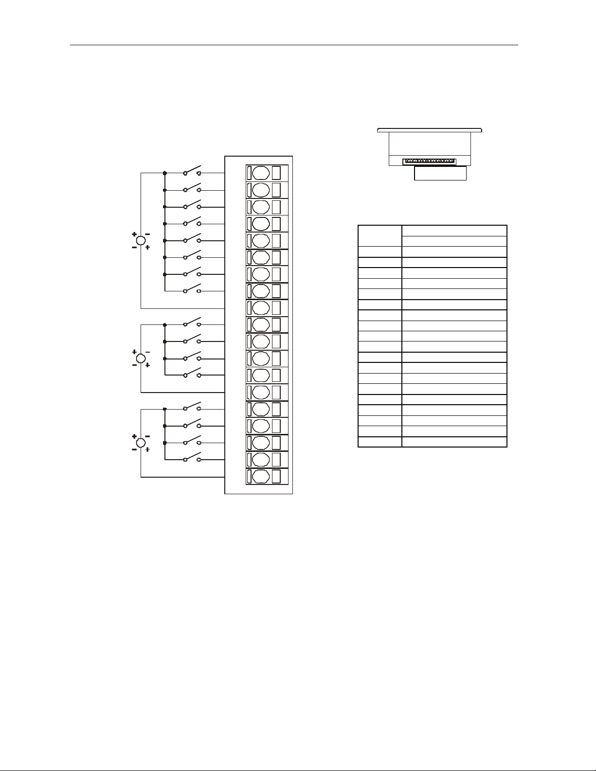
Mini Top View – Shows
Signal
001OCX004
PAGE 2 19 MAR 2003 OCX003
2 WIRING
2.1 Input I/O Connector
12-24VDC
12-24VDC
12-24VDC
12-24VDC
12-24VDC
12-24VDC
I1
I1
I2
I2
I3
I3
I4
I4
I5
I5
I6
I6
I7
I7
I8
I8
C1
C1
19
19
I10
I10
I11
I11
I12
I12
C2
C2
I13
I13
I14
I14
I15
I15
I16
I16
C3
C3
corresponding I/O pin location
Pin
I1 Input 1
I2 Input 2
I3 Input 3
I4 Input 4
I5 Input 5
I6 Input 6
I7 Input 7
I8 Input 8
C1 Common 1 (Isolated)
I9 Input 9
I10 Input 10
I11 Input 11
I12 Input 12
C2 Common 2 (Isolated)
I13 Input 13
I14 Input 14
I15 Input 15
I16 Input 16
C3 Common 3 (Isolated)
OCX003 INPUT
Information is subject to change without notice. Cscape is a trademark of Horner APG, LLC.
Page 3

OCX003 19 MAR 2003 PAGE 3
Mini Bottom View – Shows
Signal
2.2 Output
LOAD
LOAD
LOAD
LOAD
LOAD
LOAD
LOAD
LOAD
LOAD
LOAD
LOAD
LOAD
LOAD
LOAD
LOAD
LOAD
LOAD
LOAD
+
+ -
+ -
+
+ -
+ -
+ -
+ -
+ -
+
+
+ -
+ -
+ -
+ -
+ -
+ -
+ -
Q1
Q2
Q3
Q4
Q5
Q6
Q7
Q8
VA+
Q9
Q10
Q11
Q12
Q13
Q14
Q15
Q16
C4
VB+
001OCX003
corresponding I/O pin location
Pin
Q1 Output 1
Q2 Output 2
Q3 Output 3
Q4 Output 4
Q5 Output 5
Q6 Output 6
Q7 Output 7
Q8 Output 8
VA+ Load Power A
Q9 Output 9
Q10 Output 10
Q11 Output 11
Q12 Output 12
Q13 Output 13
Q14 Output 14
Q15 Output 15
Q16 Output 16
C4 Common
VB+ Load Power B
OCX003 Output
-
-
10-30VDC
-
-
10-30VDC
Information is subject to change without notice. Cscape is a trademark of Horner APG, LLC.
Page 4

To
Field
OCX Back View Connector – Shows
Signal
Note: The Voltage/Current mode switch is located directly
above each input. Moving a switch towards Pin 1* selects
20mA for the corresponding channel. Moving the switch
10VDC. Each channel must be set
up in Cscape for the desired mode in addition to the physical
+
+
Field
PAGE 4 19 MAR 2003 OCX003
2.3 Analog Input / Output
LOOP POWERED TRANSMITTER
20mA LOOP POWER
±20mA SELF POWERED TRANSMITTER
±10V SOURCE
±10V SOURCE
±
towards Pin 12 selects ±
switch settings for proper signal scaling in the PLC registers.
I1
C
I2
C
I3
C
I4
NC
NC
NC
NC
001OCX010
corresponding I/O pin location
Pin
I1 Input 1
C Common
I2 Input 2
C Common
I3 Input 3
C Common
I4 Input 4
C Common
NC No Connect
NC No Connect
NC No Connect
NC No Connect
OCX003
Analog In / Out
3 INTERNAL SCHEMATIC
I/O Connector
Digital Input
Side
iI1
C
I/O Connector
Digital Output
V+
Side
Q
VC
Specification for transient voltage suppressors used on digital output circuitry is 33V, 300W .
VCC
Controller
From
Controller
Information is subject to change without notice. Cscape is a trademark of Horner APG, LLC.
Page 5

OCX003 19 MAR 2003 PAGE 5
and for applications where it is necessary to change the
when the controller enters idle/stop mode. To avoid
exercise extreme caution when changing the default
e: ±10V or ±20mA must be set for each channel. The
60201004080
20
Scans
0
%Complete [ ]
Filter
4 CONFIGURATION
Note: The status of the I/O can be monitored in Cscape Software.
Module Setup Tab
The Module Setup is used to configure the Analog
Inputs and Analog Outputs ±10V and ±20mA modes
default states or values of the outputs when the
controller (e.g., OCS100) enters idle/stop mode.
1. For Digital Outputs: The default turns the outputs
OFF when the controller enters idle/stop mode. By
selecting the Module Setup tab, each output can be set
to either turn ON, turn OFF or to hold the last state.
Generally, most applications use the default settings.
Warning: The default turns the digital outputs OFF
injury of personnel or damages to equipment,
settings.
100
90
80
70
60
50
40
30
10
0
Digital Filtering. The illustration above demonstrates the effect of digital filtering (set with Fillter
Constant) on module response to a temperature change.
1 2 3 4 5 60 7
2. For Analog Inputs
Mod
associated slide switch on the back of the module must
match the Cscape setting for each channel.
Filter Constant: Sets the level of digital filtering according
to the following chart.
I/O Map Tab
The I/O Map describes which I/O registers are assigned.
The I/O Map is not edited by the user.
Constant
Information is subject to change without notice. Cscape is a trademark of Horner APG, LLC.
Page 6

PAGE 6 19 MAR 2003 OCX003
Digital Input Chart
5 ANALOG INPUT CONVERSION FACTOR
The following table describes how real -world inputs are scaled into the controller. Given a known input
current, the data value is configured by using the conversion factor from the table. The following formula
is used: Data = Input Current (mA) / Conversion Factor
Example: The user selects a current range of ±20mA:
1. The known input current is 14mA.
2. Using the table, the conversion factor for the current range of ±20mA is 0.000625.
3. To determine the data value, the formula is used:
Data = Input Current (mA) / Conversion F actor
22400 = 14mA / 0.000625
Conversion of Real-World Inputs into Controller
Selected Range Input Register Data Conversion Factor
+20.00 32000
±20mA
0.00 0
0.000625
-20.00 -32000
+10.00 32000
0.00 0 ±10 V
0.0003125
-10.00 -32000
6 DIGITAL INPUT / OUTPUT CHARACTERISTICS
6.1 Digital Input
.125(±±15%) V-A
0
35VDC
Information is subject to change without notice. Cscape is a trademark of Horner APG, LLC.
Page 7

OCX003 19 MAR 2003 PAGE 7
6.2 Digital Output
AMPS / CHANNEL
.5
.4
.3
.2
.1
0
0 10 20 30 40 50 60 °°C
32 50 68 86 104 122 140 °°F
Derating Chart
7 INSTALLATION / SAFETY
a. All applicable codes and standards should be followed in the installation of this product.
b. Shielded, twisted -pair wiring should be used for best performance.
c. Shields may be terminated at the module terminal strip.
d. In severe applications, shields should be tied directly to the ground block within the panel.
e. Use the following wire type or equivalent: Belden 8441 or equivalent.
For detailed installation information, refer to Mini Hardware Manual. A handy checklist is provided that
covers panel box layout requirements and minimum clearances .
8 TECHNICAL ASSISTANCE
For assistance, contact Technical Suppo rt at the following locations:
North America:
(317) 916 -4274
www.heapg.com.
Europe:
(+) 353-21-4321-266
www.horner-apg.com
Information is subject to change without notice. Cscape is a trademark of Horner APG, LLC.
Page 8

PAGE 8 19 MAR 2003 OCX003
NOTES
Information is subject to change without notice. Cscape is a trademark of Horner APG, LLC.
 Loading...