

Page 1
RF12 Program V1.1
RF12B programming guide
1. Brief description
RF12B is a low cost FSK transceiver IC witch integrated all RF functions in a
single chip. It only need a MCU, a crystal, a decouple capacitor and antenna to
build a hi reliable FSK transceiver system. The operation frequency can cover 400
to 1000MHz.
RF12B supports a command interface to setup frequency, deviation, output power
and also data rate. No need any hardware adjustment when using in frequency-hopping
applications
RF12B can be used in applications such as remote control toys, wireless alarm,
wireless sensor, wireless keyboard/mouse, home-automation and wireless data
collection.
2. Commands
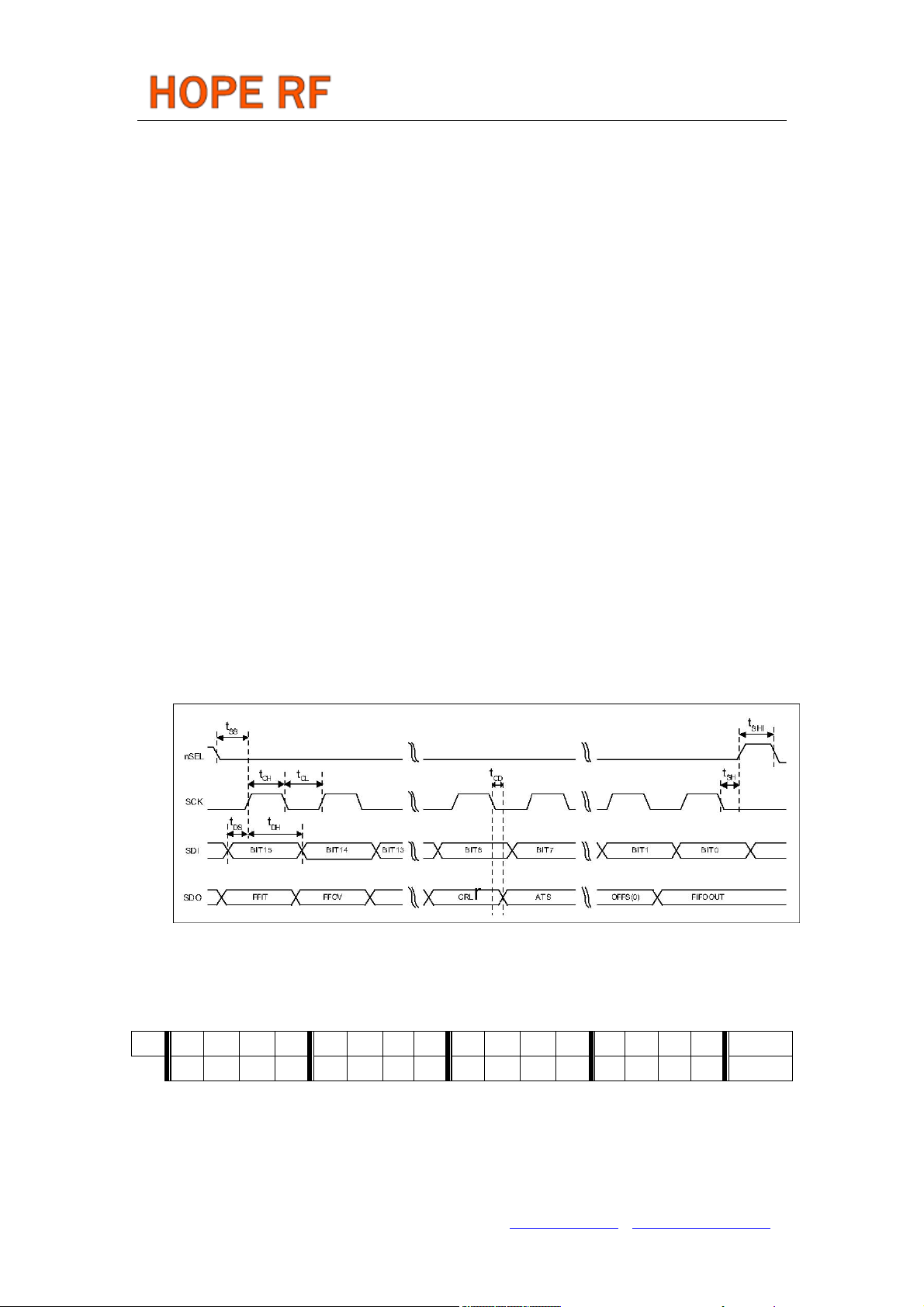
1. Timing diagram
2. Configuration Setting Command
bit 15 14 13 12 11 10 9 8 7 6 5 4 3 2 1 0 POR
1 0 0 0 0 0 0 0 el ef b1 b0 x3 x2 x1 x0 8008h
e l: Enable TX register
e f: Enable RX FIFO buffer
Tel: +86-755-82973805 Fax: +86-755-82973550 E-mail: [email protected] http://www.hoperf.com
Page 2
RF12 Program V1.1
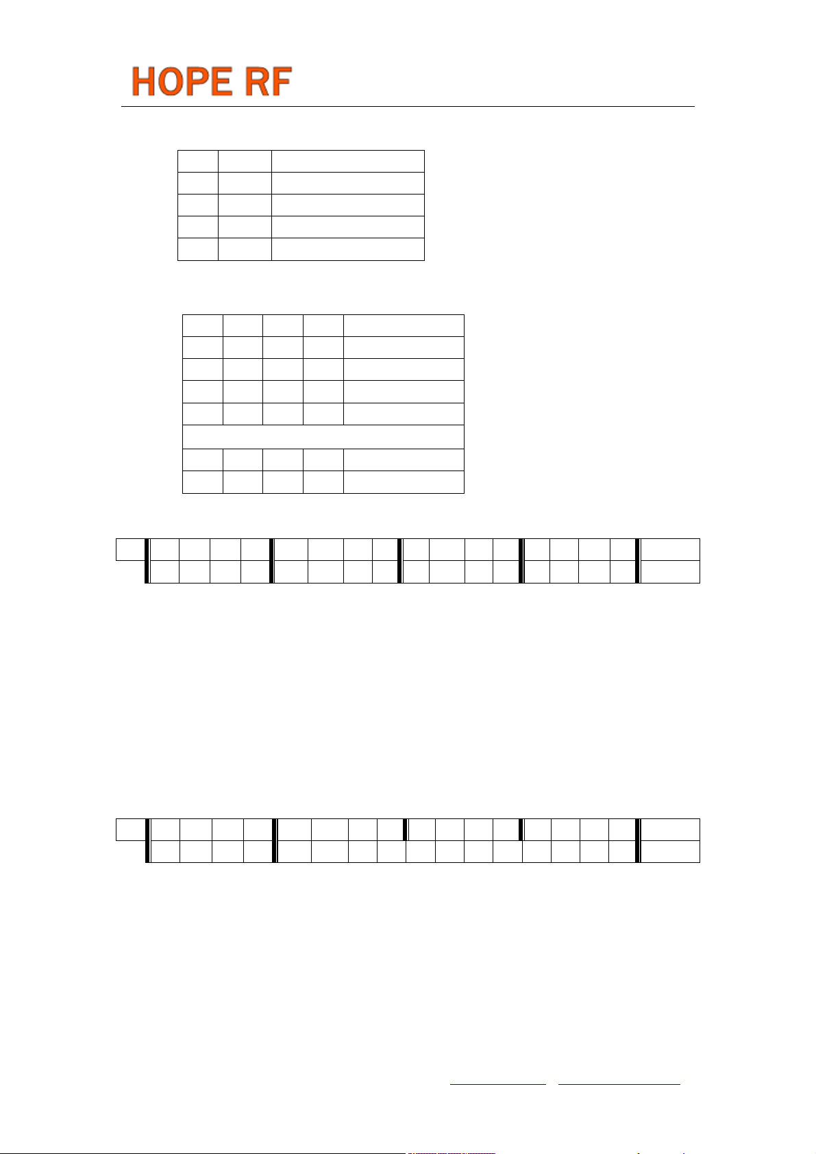
b1..b0: select band
b1 b0 band[MHz]
0 0 Reserved
0 1 433
1 0 868
1 1 915
x3..x0: select crystal load capacitor
x3 x2 x1 x0
0 0 0 0 8.5
0 0 0 1 9.0
0 0 1 0 9.5
0 0 1 1 10.0
…… ……
1 1 1 0 15.5
1 1 1 1 16.0
load capacitor [pF]
3. Power Management Command
bit 15 14 13 12 11 10 9 8 7 6 5 4 3 2 1 0 POR
1 0 0 0 0 0 1 0 er ebb et es ex eb ew dc 8208h
er: Enable receiver
ebb:Enable base band block
et: Enable transmitter
es: Enable synthesizer
ex: Enable crystal oscillator
eb: Enable low battery detector
ew: Enable wake-up timer
dc: Disable clock output of CLK pin
4. Frequency Setting Command
bit 15 14 13 12 11 10 9 8 7 6 5 4 3 2 1 0 POR
1 0 1 0 f11 f10 f9 f8 f7 f6 f5 f4 f3 f2 f1 f0 A680h
f11..f0: Set operation frequency:
433band: Fc=430+F*0.0025 MHz
868band: Fc=860+F*0.0050 MHz
915band: Fc=900+F*0.0075 MHz
Fc is carrier frequency and F is the frequency parameter. 36≤F≤3903
Tel: +86-755-82973805 Fax: +86-755-82973550 E-mail: [email protected] http://www.hoperf.com
Page 3
RF12 Program V1.1
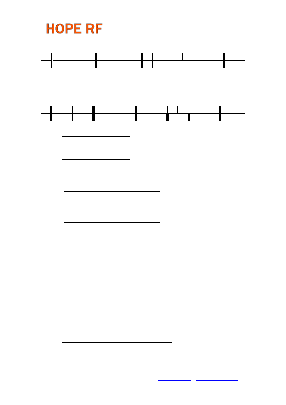
5. Data Rate Command
bit 15 14 13 12 11 10 9 8 7 6 5 4 3 2 1 0 POR
1 1 0 0 1 0 0 0 cs r6 r5 r4 r3 r2 r1 r0 C623h
r6..r0: Set data rate:
BR=10000000/29/(R+1)/(1+cs*7)
6. Receiver Control Command
bit 15 14 13 12 11 10 9 8 7 6 5 4 3 2 1 0 POR
1 1 0 0 0 P16 d1 d0 i2 i1 i0 g1 g0 r2 r1 r0 9080h
P16: select function of pin16
P16
0
Interrupt input
1 VDI output
i2..i0:select baseband bandwidth
i2 i1 i0 Baseband Bandwidth [kHz]
0 0 0 reserved
0 0 1 400
0 1 0 340
0 1 1 270
1 0 0 200
1 0 1 134
1 1 0 67
1 1 1 reserved
d1..d0: select VDI
d1 d0 Response
0 0 Fast
0 1 Medium
1 0 Slow
1 1 Always on
response time
g1..g0: select LNA gain
g1 g0 LNA gain (dBm)
0 0 0
0 1 -6
1 0 -14
1 1 -20
Tel: +86-755-82973805 Fax: +86-755-82973550 E-mail: [email protected] http://www.hoperf.com
Page 4
RF12 Program V1.1
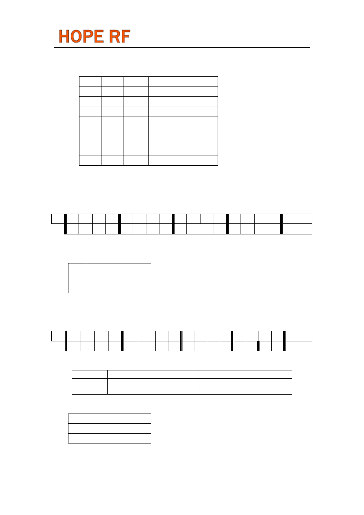
r2..r0: select DRSSI threshold
r2 r1 r0 RSSIsetth [dBm]
0 0 0 -103
0 0 1 -97
0 1 0 -91
0 1 1 -85
1 0 0 -79
1 0 1 -73
1 1 0 Reserved
1 0 1 Reserved
The actual DRSSI threshold is related to LNA setup:
RSSI
= RSSI
th
setth
+ G
LNA.
7. Data Filter Command
bit 15 14 13 12 11 10 9 8 7 6 5 4 3 2 1 0 POR
1 1 0 0 0 0 1 0 al ml 1 s
f2 f1 f0 C22Ch
1
al: Enable clock recovery auto-lock
ml: Enable clock recovery fast mode
s: select data filter type
s Filter type
Digital filter
0
Analog RC filter
1
f1..f0: Set DQD threshold
8. FIFO and Reset Mode Command
bit 15 14 13 12 11 10 9 8 7 6 5 4 3 2 1 0 POR
1 1 0 0 1 0 1 0 f3 f2 f1 f0 sp al ff dr CA80h
f3..f0: Set FIFO interrupt level
sp: Select the length of the synchron pattern:
sp Byte1 Byte0 (POR) Synchron Pattern (Byte1+Byte0)
0 2Dh D4h 2DD4h
1 Not used D4h D4h
al: select FIFO fill start condition
al condition
0 Sync-word
1 Always
ff: Enable FIFO fill
dr: Disable hi sensitivity reset mode
Tel: +86-755-82973805 Fax: +86-755-82973550 E-mail: [email protected] http://www.hoperf.com
Page 5
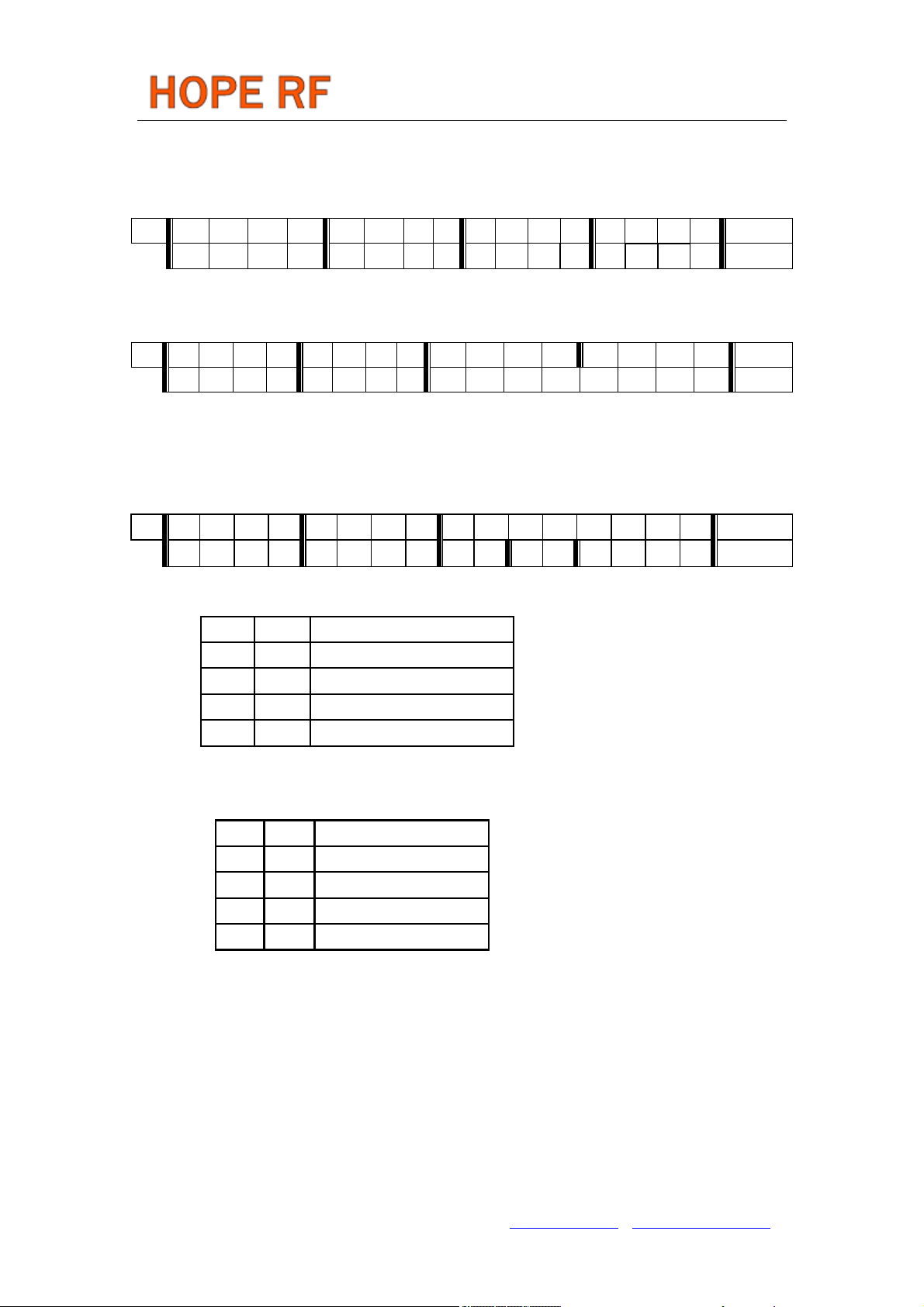
RF12 Program V1.1
9. Synchron pattern Command
bit 15 14 13 12 11 10 9 8 7 6 5 4 3 2 1 0 POR
1 1 0 0 1 1 1 0 b7 b6 b5 b4 b3 b2 b1 b0 CED4h
This command is used to reprogram the synchronic pattern;
10. Receiver FIFO Read Command
bit 15 14 13 12 11 10 9 8 7 6 5 4 3 2 1 0 POR
1 0 1 1 0 0 0 0 0 0 0 0 0 0 0 0 B000h
This command is used to read FIFO data when FFIT interrupt generated. FIFO data
th
output starts at 8
SCK period.
11. AFC Command
bit 15 14 13 12 11 10 9 8 7 6 5 4 3 2 1 0 POR
1 1 0 0 0 1 0 0 a1 a0 rl1 rl0 st fi oe en C4F7h
a1..a0: select AFC auto-mode:
a1 a0
0 0 Controlled by MCU
0 1 Run once at power on
1 0 Keep offset when VDI hi
1 1 Keeps independently from VDI
rl1..rl0: select range limit
r1 r0
0 0 No restriction
0 1 +15/-16
1 0 +7/-8
1 1 +3-4
range(fres)
st: st goes hi will store offset into output register
fi: Enable AFC hi accuracy mode
oe: Enable AFC output register
en: Enable AFC funcition
fres
315,433band: 2.5kHz
868band: 5kHz
915band: 7.5kHz
Tel: +86-755-82973805 Fax: +86-755-82973550 E-mail: [email protected] http://www.hoperf.com
Page 6
RF12 Program V1.1
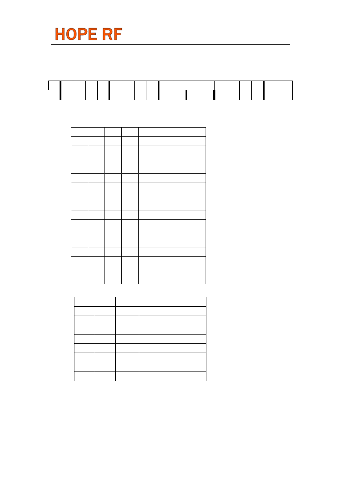
12. TX Configuration Control Command
bit 15 14 13 12 11 10 9 8 7 6 5 4 3 2 1 0 POR
1 0 0 1 1 0 0 mp
m3 m2 m1 m0
0
p2 p1 p0
9800h
m: select modulation polarity
m2..m0: select frequency deviation:
m3 m2 m1 m0
0 0 0 0 15
0 0 0 1 30
0 0 1 0 45
0 0 1 1 60
0 1 0 0 75
0 1 0 1 90
0 1 1 0 105
0 1 1 1 120
1 0 0 0 135
1 0 0 1 150
1 0 1 0 165
1 0 1 1 180
1 1 0 0 195
1 1 0 1 210
1 1 1 0 225
frequency deviation [kHz]
1 1 1 1 240
p2..p0: select output power
p2 p1 p0 Output power[dBm]
0 0 0 0
0 0 1 -3
0 1 0 -6
0 1 1 -9
1 0 0 -12
1 0 1 -15
1 1 0 -18
1 0 1 -21
Tel: +86-755-82973805 Fax: +86-755-82973550 E-mail: [email protected] http://www.hoperf.com
Page 7
RF12 Program V1.1
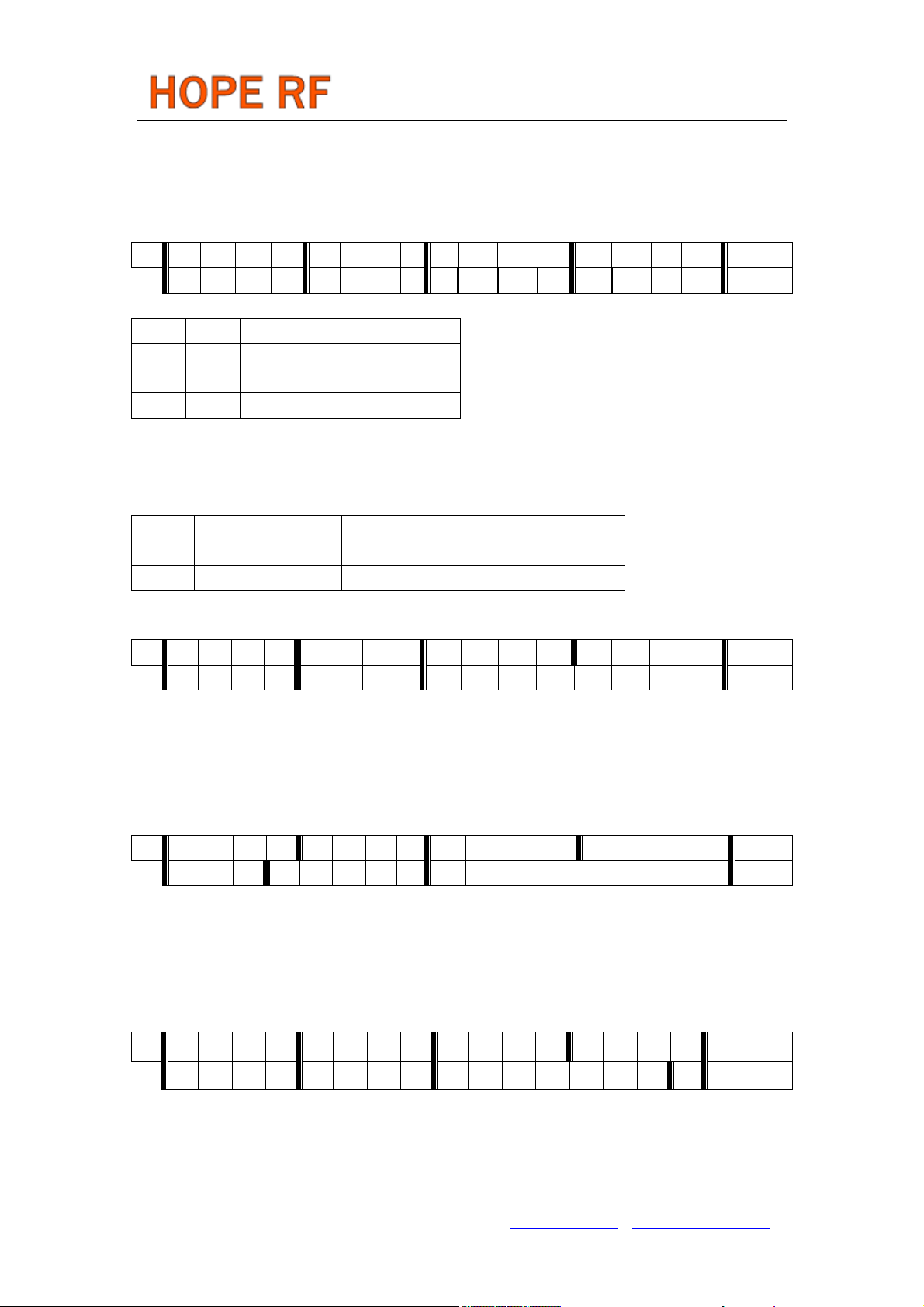
13. PLL Setting Command
bit 15 14 13 12 11 10 9 8 7 6 5 4 3 2 1 0 POR
1 1 0 0 1 1 0 0 0 ob1 ob0 1 ddy ddit 1 bw0 CC77h
ob1-ob0: Microcontroller output clock buffer rise and fall time control.
ob1 ob0 Selected u C CLK frequency
0 0 5 or 10 MHz (recommended)
0 1 3.3 MHz
1 X 2.5 MHz or less
ddy: phase detector delay enable.
ddi: disables the dithering in the PLL loop.
bw1-bw0: select PLL bandwidth
bw0 Max bit rate [kbps] Phase noise at 1MHz offset [dBc/Hz]
0 86.2 -107
1 256 -102
14. Transmitter Register Write Command
bit 15 14 13 12 11 10 9 8 7 6 5 4 3 2 1 0 POR
1 0 1 1 1 0 0 0 t7 t6 t5 t4 t3 t2 t1 t0 B8AAh
This command is use to write a data byte to RF12 and then RF12 transmit it
15. Wake-Up Timer Command
bit 15 14 13 12 11 10 9 8 7 6 5 4 3 2 1 0 POR
1 1 1 r4 r3 r2 r1 r0 m7 m6 m5 m4 m3 m2 m1 m0 E196h
The wake-up period is determined by:
T
= M * 2R [ms]
wake-up
For continual operation, bit ‘et’ must be cleared and set
16. Low Duty-Cycle Command
bit 15 14 13 12 11 10 9 8 7 6 5 4 3 2 1 0 POR
1 1 0 0 1 0 0 0 d6 d5 d4 d3 d2 d1 d0 en C8OEh
d6..d0: Set duty cycle
D.C.= (D * 2 +1) / M *100%
Tel: +86-755-82973805 Fax: +86-755-82973550 E-mail: [email protected] http://www.hoperf.com
Page 8
RF12 Program V1.1
en:Enable low duty cycle mode
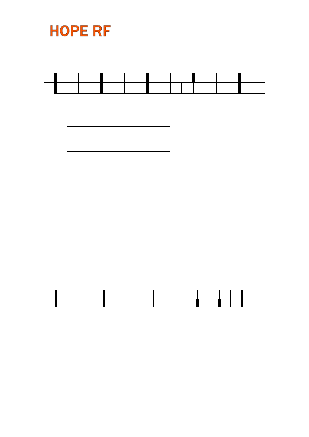
17. Low Battery Detector and Microcontroller Clock Divider Command
bit 15 14 13 12 11 10 9 8 7 6 5 4 3 2 1 0 POR
1 1 0 0 0 0 0 0 d2 d1 d0 0 v3 v2 v1 v0 C000h
d2..d0: select frequency of CLK pin
d2 d1 d0 Clock frequency[MHz]
0 0 0 1
0 0 1 1.25
0 1 0 1.66
0 1 1 2
1 0 0 2.5
1 0 1 3.33
1 1 0 5
1 1 1 10
CLK signal is derive form crystal oscillator and it can be applied to MCU clock in to save
a second crystal.
If not used, please set bit “dc” to disable CLK output
To integrate the load capacitor internal can not only save cost, but also adjust reference
frequency by software
v3..v0: Set threshold voltage of Low battery detector:
Vlb=2.2+V*0.1 [V]
18. Status Read Command
bit 15 14 13 12 11 10 9 8 7 6 5 4 3 2 1 0 POR
0 x x x x x x x x x x x x x x x -
This command starts with a 0 and be used to read internal status register
Tel: +86-755-82973805 Fax: +86-755-82973550 E-mail: [email protected] http://www.hoperf.com
Page 9
RF12 Program V1.1
N
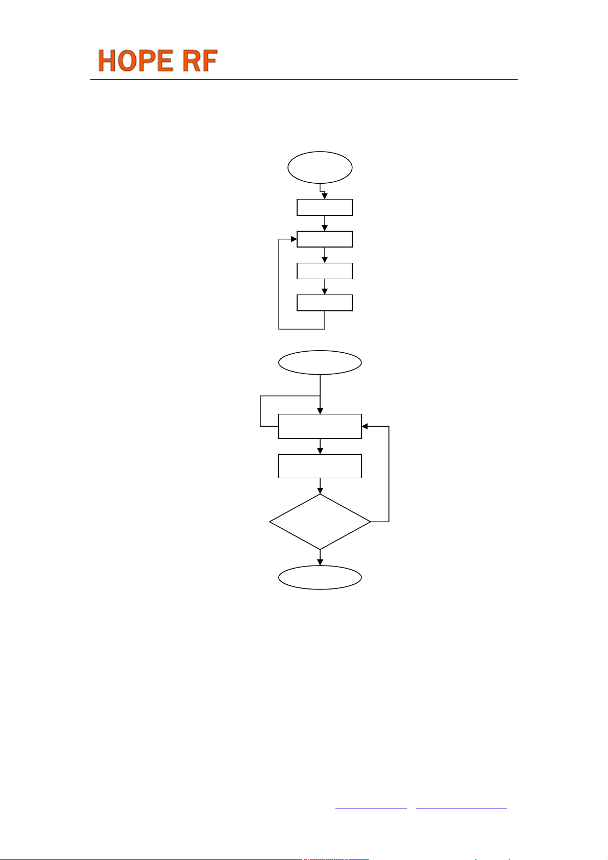
3. Demo flow diagram
Transmitter:
DEMO
Init RF12B
Open TX
Send data
Close TX
Send data
Wait nIRQ low
Write a byte
Package
Y
return
Note: Initialize RF12B and open transmitter, RF12B will transm
w
hen transmit over, then MCU can write next byte to transmit
it a byte and pull nIRQ low
Tel: +86-755-82973805 Fax: +86-755-82973550 E-mail: [email protected] http://www.hoperf.com
Page 10
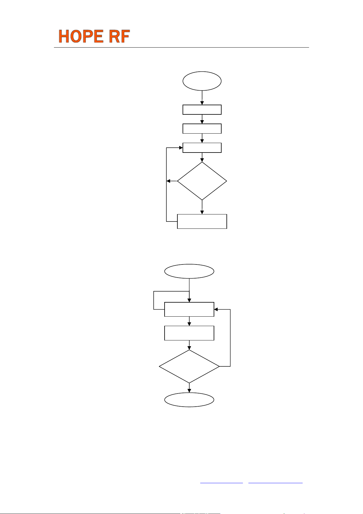
N
p
N
Receiver:
RF12 Program V1.1
DEMO
Init RF12B
Open RX
Receive data
Check
ass?
Y
Indicate receive
Receive data
Wait nIRQ low
Read FIFO data
Data recive
Y
return
Note: After RF12B initialization, Open FIFO receive mode and wait nIRQ low, only then MCU
e
can r ad received and stored in FIFO data. For next package receive, please reset FIFO.
Tel: +86-755-82973805 Fax: +86-755-82973550 E-mail: [email protected] http://www.hoperf.com
Page 11
RF12 Program V1.1
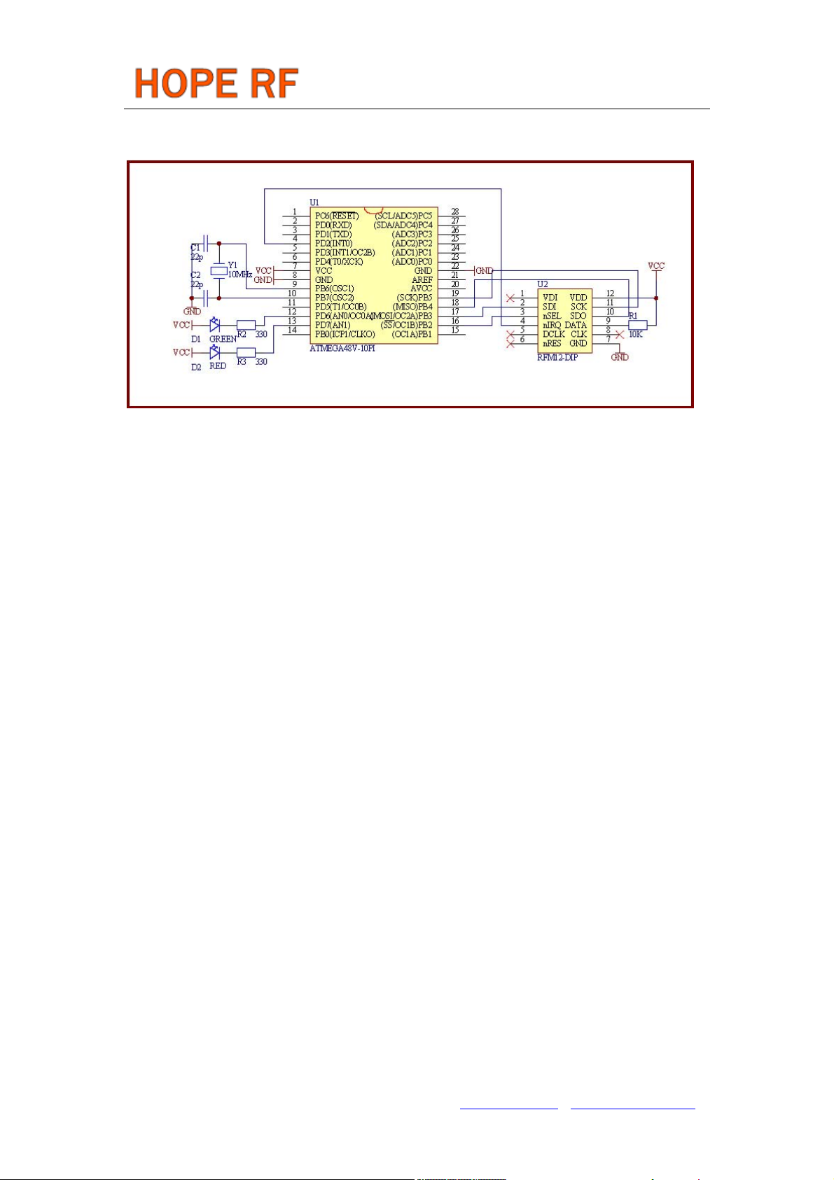
4. Example 1(for AVR microcontroller)
RF12 transmitter de o: m
/*
; copyright (c) 2006
;Title RF12 TX si
;Company: Hope micro
;Author: Tank
;Current version: v1.0
;Date: 2006-11-13
;processor ATMEGA48
;Clock: 10MHz Crystal
;Contact: +86-0755-86106557
;E
Connections
ATMEGA48 SIDE RF12 S
SCK--------------->SCK
MISO--------------->SDO
MOSI--------------->SDI
INT0<-----------
PD6: LED GREEN
*/
SS--------------->nSEL
PD7: LED RED
-MAIL: [email protected]
IDE
----nIRQ
mple example based on AVR C
electronic Co.,Ltd.
Tel: +86-755-82973805 Fax: +86-755-82973550 E-mail: [email protected] http://www.hoperf.com
Page 12

RF12 Program V1.1
nclude <mega48.h>
#i
efine DDR_IN 0
#d
#define DDR_OUT 1
#define PORT_SEL PORTB
#d
efine PIN_SEL PINB
#define DDR_SEL DDRB
#define PORT_SDI PORTB
#d
efine PIN_SDI PINB
#define DDR_SDI DDRB
#define PORT_SCK PORTB
#d
efine PIN_SCK PINB
#define DDR_SCK DDRB
#define PORT_SDO PORTB
#d
efine PIN_SDO PINB
#define DDR_SDO DDRB
#define PORT_DATA PORTD
#define
PIN_DATA PIND
#define DDR_DATA DDRD
#define PB7 7//--\
#define PB6 6// |
#define RFXX_SCK 5// |
#define RFXX_SDO 4// |RF
_PORT
#define RFXX_SDI 3// |
#define RFXX_SEL 2// |
#d
efine NC 1// |
#define PB0 0//--/
#define SEL_OUTPUT() DDR_SEL |= (1<<RFXX_SEL)
#d
efine HI_SEL() PORT_SEL|= (1<<RFXX_SEL)
#define LOW_SEL() PORT_SEL&=~(1<<RFXX_SEL)
#define SDI_OUTPUT() DDR_SDI |= (1<<RFXX_SDI)
#d
efine HI_SDI() PORT_SDI|= (1<<RFXX_SDI)
#define LOW_SDI() PORT_SDI&=~(1<<RFXX_SDI)
#d
efine SDO_INPUT() DDR_SDO&= ~(1<<RFXX_SDO)
Tel: +86-755-82973805 Fax: +86-755-82973550 E-mail: [email protected] http://www.hoperf.com
Page 13

RF12 Program V1.1
#define SDO_HI() PIN_SDO&(1<<RFXX_SDO)
#define SCK_OUTPUT() DDR_SCK |= (1<<RFXX_SCK)
efine HI_SCK() PORT_SCK|= (1<<RFXX_SCK)
#d
#define LOW_SCK() PORT_SCK&=~
(1<<RFXX_SCK)
#define RF12_DATA 4//PD4
#d
efine DATA_OUT DDR_DATA|=1<<RF12_DATA
#define HI_DATA PORT_DATA|=1<<R
F12_DATA
#d
efine LEDG_OUTPUT() DDRD|=~(1<<6)
#define LEDR_OUTPUT() DDRD|=~(1<<7)
#define LEDG_ON() PORTD&=~(1<<6)
#define LEDG_OFF() PORTD|=~(1<<6)
#define
#defin
LEDR_ON() PORTD&=~(1<<7)
e LEDR_OFF() PORTD|=~(1<<7)
void RFXX_POR
T_INIT(void){
HI_SEL();
HI_SDI();
LOW_SCK();
SEL_OUTPUT();
SDI_OUTPUT();
DO_INPUT();
S
SCK_OUTPUT();
}
unsigned int RFXX_WRT_
unsigned char i;
unsigned int temp
CMD(unsigned int aCmd){
;
LOW_SCK();
LOW_SEL();
for(i=0;i<16;i++){
temp<<=1;
if(SDO_HI
temp|=0x00
()){
01;
}
LOW_SCK();
if(aCmd&0x800
0){
HI_SDI();
}else{
LOW_SDI()
;
}
Tel: +86-755-82973805 Fax: +86-755-82973550 E-mail: [email protected] http://www.hoperf.com
Page 14

RF12 Program V1.1
HI_SCK();
aCmd<<=1;
};
LOW_SCK();
SEL();
HI_
return(temp);
}
void RF12_INIT(void){
RFXX_WRT_CMD(0x80D7);//EL,EF,433band,1
RFXX_WRT_CMD(0x8239);//!er,!ebb,
ET,ES,EX,!eb,!ew,DC
2.0pF
RFXX_WRT_CMD(0xA640);//A140=430.8MHz
RFXX_WRT_CMD(0xC647);//4.8kbps
RFXX_WRT_CMD(0x94A0);//VDI,FAST,134kHz,0dB
RFXX_WRT_CMD(0xC2AC);//AL,!ml,DIG,DQ
D4
m,-103dBm
RFXX_WRT_CMD(0xCA81);//FIFO8,SYNC,!ff,DR
RFXX_WRT_CMD(0xCED4);//SYNC=2DD4;
RFXX_WRT_CMD(0xC483);//@PWR,NO RSTRIC,!st,!fi,OE,EN
RFXX_WRT_CMD(0x9850);//!mp,9810=
RFXX_WRT_CMD(0xCC77);//OB1,OB0,
30kHz,MAX OUT
!lpx,!ddy,DDIT,BW0
RFXX_WRT_CMD(0xE000);//NOT USE
RF
XX_WRT_CMD(0xC800);//NOT USE
RFXX_WRT_CMD(0xC040);//1.66MHz,2.2V
}
void RF12_SEND(unsigned char aByte)
w
hile(PIND&(1<<2));//wait for previously TX over
RFXX_WRT_CMD(0xB800+aByte);
{
}
void Delay_ms(unsig
ned char amS){
unsigned char i;
u
nsigned int j;
for(i=0;i<amS;i
++)for(j=0;j<914;j++);
}
void main(void)
{
un
signed int i,j;
unsigned char C
hkSum;
#asm("cli");
DD
RB=0x00;//PB INPUT;
DDRD=0x00;//PD INPUT;
//POWER ON ind
ication: both LEDR and LEDG blink 3 times
LEDG_OFF();
Tel: +86-755-82973805 Fax: +86-755-82973550 E-mail: [email protected] http://www.hoperf.com
Page 15

RF12 Program V1.1
LEDR_OFF();
LEDG_OUTPUT();
LEDR_OUTPUT();
for(i=0;i<3;i+
Delay_ms(200)
+){
;
LEDG_ON();
LEDR_ON();
Delay_ms(200);
L
EDG_OFF();
LE
DR_OFF();
}
LE
DG_OFF();
LEDR_OFF();
RFXX_PORT_INIT
();
RF12_INIT();
DDRD|=(1<<RF12_DATA);
PO
RTD|=(1<<RF12_DATA);// SET nFFS pin HI when using TX register
DD
RD&=~(1<<2); //PD2(INT0)
while(1){
LEDR_ON();
RF
RFXX_WRT_CM
XX_WRT_CMD(0x0000);//read status register
D(0x8239);//!er,!ebb,ET,ES,EX,!eb,!ew,DC
ChkSum=0;
RF12_SEND(0xAA);//PREAMBLE
RF12_SEND(0xAA);//PREAMBLE
RF12_SEND(0xAA);//PREAMBLE
RF12_SEND(0x2D);//SYNC HI BYTE
RF12_SEND(0xD4);//SY
NC LOW BYTE
RF12_SEND(0x30);//DATA BYTE 0
ChkSum+=0x30;
RF12_SEND(0x31);//D
ATA BYTE 1
ChkSum+=0x31;
RF12_SEND(0x32);
ChkSum+=0x32;
RF12_SEND(0x33);
ChkSum+=0x33;
RF12_SEND(0x34);
Tel: +86-755-82973805 Fax: +86-755-82973550 E-mail: [email protected] http://www.hoperf.com
Page 16

RF12 Program V1.1
ChkSum+=0x34;
RF12_SEND(0x35);
ChkSum+=0x35;
RF12_SEND(0x36);
ChkSum+=0x36;
RF12_SEND(0x37);
ChkSum+=0x37;
RF12_SEND(0x38);
ChkSum+=0x38;
RF12_SEND(0x39);
ChkSum+=0x39;
RF12_SEND(0x3A);
ChkSum+=0x3A;
RF12_SEND(0x3B);
ChkSum+=0x3B;
RF12_SEND(0x3C);
ChkSum+=0x3C;
RF12_SEND(0x3D);
ChkSum+=0x3D;
RF12_SEND(0x3E);
ChkSum+=0x3E;
RF12_SEND(0x3F); //DATA BYTE 15
ChkSum+=0x3F;
RF12_SEND(ChkSum); //send chek
sum
RF12_SEND(0xAA);//DUMMY BYTE
RF12_SEND(0xAA);//DUMMY BYTE
RF12_SEND(0xAA);//DUMMY
BYTE
RFXX_WRT_CMD(
0x8201);
LEDR_OFF();
LE
fo
DG_OFF();
r(i=0;i<10000;i++)for(j=0;j<123;j++);//sleep 1 second appr.
};
}
RF12 receiver demo
/*
; copyright (c) 2006
;Title RF12 RX si
;Company: Hope micro
mple example based on AVR C
electronic Co.,Ltd.
;Author: Tank
Tel: +86-755-82973805 Fax: +86-755-82973550 E-mail: [email protected] http://www.hoperf.com
Page 17

RF12 Program V1.1
;Current version: v1.0
;Date: 2006-11-17
;processor ATMEGA48
;Clock: 10MHz Crystal
;Contact: +86-0755-86106557
;E
-MAIL: [email protected]
Connections
ATMEGA48 SIDE RF12 S
SCK--------------->SCK
IDE
MISO<---------------SDO
MOSI--------------->SDI
SS--------------->nSEL
P
INT0<-----------
D4--------------->FSK/DATA
----nIRQ
PD6: LED GREEN
PD7: LED RED
*/
#i
nclude <mega48.h>
#d
efine DDR_IN 0
#define DDR_OUT 1
#define PORT_SEL PORTB
#d
efine PIN_SEL PINB
#define DDR_SEL DDRB
#define PORT_SDI PORTB
#d
efine PIN_SDI PINB
#define DDR_SDI DDRB
#define PORT_SCK PORTB
#d
efine PIN_SCK PINB
#define DDR_SCK DDRB
#define PORT_SDO PORTB
#d
efine PIN_SDO PINB
#define DDR_SDO DDRB
Tel: +86-755-82973805 Fax: +86-755-82973550 E-mail: [email protected] http://www.hoperf.com
Page 18

RF12 Program V1.1
#define PORT_IRQ PORTD
efine PIN_IRQ PIND
#d
#define DDR_IRQ DDRD
#define PORT_DATA PORTD
#define
PIN_DATA PIND
#define DDR_DATA DDRD
#define PB7 7//--\
#define PB6 6// |
#define RFXX_SCK 5// |
#define RFXX_SDO 4// |RF
_PORT
#define RFXX_SDI 3// |
#define RFXX_SEL 2// |
efine NC 1// |
#d
#define PB0 0//--/
#define SEL_OUTPUT() DDR_SEL |= (1<<RFXX_SEL)
#d
efine HI_SEL() PORT_SEL|= (1<<RFXX_SEL)
#define LOW_SEL() PORT_SEL&=~(1<<RFXX_SEL)
#define SDI_OUTPUT() DDR_SDI |= (1<<RFXX_SDI)
#d
efine HI_SDI() PORT_SDI|= (1<<RFXX_SDI)
#define LOW_SDI() PORT_SDI&=~(1<<RFXX_SDI)
#define SDO_INPUT() DDR_SDO&= ~(1<<RFXX_SDO)
#d
efine LOW_SDO() PORT_SDO&= (1<<RFXX_SDO)
#define SDO_HI() PIN_SDO&(1<<RFXX_SDO)
#define SCK_OUTPUT() DDR_SCK |= (1<<RFXX_SCK)
#d
efine HI_SCK() PORT_SCK|= (1<<RFXX_SCK)
#define LOW_SCK() POR
T_SCK&=~(1<<RFXX_SCK)
#define RF12_IRQ 2
#d
efine IRQ_IN() DDR_IRQ &=~(1<<RF12_IRQ)
#define WAIT_IRQ_LOW() while(PIND&
(1<<RF12_IRQ))
#define RF12_DATA 4//PD4
#d
efine DATA_OUT() DDR_DATA|=1<<RF12_DATA
#define HI_DATA() PORT_DATA|=1<<R
F12_DATA
#d
efine LEDG_OUTPUT() DDRD|=~(1<<6)
#define LEDR_OUTPUT() DDRD|=~(1<<7)
Tel: +86-755-82973805 Fax: +86-755-82973550 E-mail: [email protected] http://www.hoperf.com
Page 19

RF12 Program V1.1
#define LEDG_ON() PORTD&=~(1<<6)
#define LEDG_OFF() PORTD|= (1<<6)
#define
#defin
LEDR_ON() PORTD&=~(1<<7)
e LEDR_OFF() PORTD|= (1<<7)
void RFXX_POR
T_INIT(void){
HI_SEL();
HI_SDI();
LOW_SCK();
//SET nFFS pin
HI when using FIFO
HI_DATA();
SEL_OUTPUT();
SDI_OUTPUT();
SDO_INPUT()
SCK_OUTPUT();
I
RQ_IN();
;
DATA_OUT();
}
unsigned int RFXX_WRT_CM
unsigned
char i;
unsigned int temp
D(unsigned int aCmd){
;
temp=0;
LOW_SCK();
LOW_SEL();
for(i=0;i<16;i+
if(aCmd&0x800
+){
0){
HI_SDI();
}else{
LOW_SDI()
;
}
HI_SCK();
temp<<=1;
if(SDO_HI
temp|=0x000
}
()){
1;
LOW_SCK();
aCmd<<=1;
};
HI_
SEL();
return(temp);
}
Tel: +86-755-82973805 Fax: +86-755-82973550 E-mail: [email protected] http://www.hoperf.com
Page 20

RF12 Program V1.1
void RF12_INIT(void){
RFXX_WRT_CMD(0x80D7);//EL,EF,433band,1
RFXX_WRT_CMD(0x82D9);//!er,!ebb,
ET,ES,EX,!eb,!ew,DC
2.0pF
RFXX_WRT_CMD(0xA640);//A140=430.8MHz
RFXX_WRT_CMD(0xC647);//4.8kbps
RFXX_WRT_CMD(0x94A0);//VDI,FAST,134kHz,0dB
RFXX_WRT_CMD(0xC2AC);//AL,!ml,DIG,DQ
D4
m,-103dBm
RFXX_WRT_CMD(0xCA81);//FIFO8,SYNC,!ff,DR
RFXX_WRT_CMD(0xCED4);//SYNC=2DD4;
RFXX_WRT_CMD(0xC483);//@PWR,NO RSTRIC,!st,!fi,OE,EN
RFXX_WRT_CMD(0x9850);//!mp,9810=
RFXX_WRT_CMD(0xCC77);//OB1,OB0,
30kHz,MAX OUT
!lpx,!ddy,DDIT,BW0
RFXX_WRT_CMD(0xE000);//NOT USE
RFXX_WRT
RFXX_WRT_CMD(0xC040);//1.66MHz
_CMD(0xC800);//NOT USE
,2.2V
}
unsigned char RF12_
RECV(void){
unsigned int FIFO_data;
WAIT_IRQ_LOW();
RFXX_WRT_CMD(0x0000);
F
IFO_data=RFXX_WRT_CMD(0xB000);
return(FIFO_data&0x00FF);
}
void Delay_ms(unsig
ned char amS){
unsigned char i;
u
nsigned int j;
for(i=0;i<amS;i
++)for(j=0;j<914;j++);
}
void main(void)
{
un
signed char i;
unsigned char ChkSum;
//POWER ON in
dication: both LEDR and LEDG blink 3 times
LEDG_OFF();
LEDR_OFF();
LE
DG_OUTPUT();
LEDR_OUTPUT();
for(i=0;i<3;i+
Delay_ms(200)
+){
;
LEDG_ON();
LEDR_ON();
Tel: +86-755-82973805 Fax: +86-755-82973550 E-mail: [email protected] http://www.hoperf.com
Page 21

RF12 Program V1.1
Delay_ms(200);
EDG_OFF();
L
LE
DR_OFF();
}
LEDG_OFF();
LEDR_OFF();
//
Initialize command port
RFXX_PORT_INIT();
//
Initialize RF12 chip
RF12_INIT();
Init FIFO
//
RFXX_WRT_CMD(0xCA
81);
while(1){
//Enable FIFO
RFXX_WRT_
CMD(0xCA83);
ChkSum=0;
//Receive payload data
for(i=0;i
ChkSum+=RF12_RECV();
<16;i++){
}
//R
eceive Check sum
i=RF12_RECV();
//
RFXX_WRT_CMD(0xCA8
Disable FIFO
1);
//Package chkec
k
if(ChkSum==i){
LEDG_ON();
Delay_
LEDG_OFF();
}
}
ms(200);
}
Tel: +86-755-82973805 Fax: +86-755-82973550 E-mail: [email protected] http://www.hoperf.com
Page 22
RF12 Program V1.1
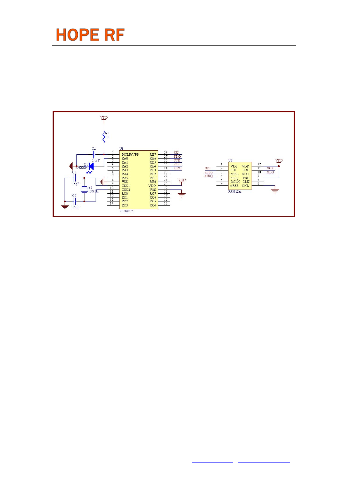
5. Example 2(for PIC microcontroller)
RF transmitter demo: 12
/**********************************************************
copyright (c) 2006
Title: RFM12B transmitter
Current version: v1.0
Function: Package send De
Processor PIC16F73
Clock: 10MHz Cry
Operate frequency: 434MHz
Data rate: 4.8kbps
Package size: 23byte
Author: Robben
Company: Hope microelectronic C
Contact: +86-0755-8610
E-MAIL: [email protected]
Date:
******************************************************/
**
#include "pic.h"
pedef unsigned char uchar;
ty
typedef unsigned int uint;
#define SDI RB7
#define SDO RB6
efine SCK RB5
#d
2006-11-21
simple example based on PIC C
mo
DIP-28
stal
o.,Ltd.
6557
Tel: +86-755-82973805 Fax: +86-755-82973550 E-mail: [email protected] http://www.hoperf.com
Page 23

RF12 Program V1.1
#define nSEL RB4
#define SDI_OUT() TRISB7=0
#define SDO_IN() TRISB6=1
efine SCK_OUT() TRISB5=0
#d
#define nSEL_OUT()
TRISB4=0
void Init_RF12(void);
void Write0( void );
void Write1( void );
void WriteCMD( uint CMD
);
void DelayUs( uint us );
id DelayMs(uint ms);
vo
void WriteFSKbyte(
uchar DATA );
__CONFIG(0x3FF2);
void Init_RF12(
void)
{
nSEL_OUT();
SDI_OUT();
SDO_IN();
SCK_OUT(
);
nSEL=1;
SDI=1;
SCK=0;
WriteCMD(0x80D8);//en
WriteCMD(0x8208);//Tu
WriteCMD(0xA640);//
able register,433MHz,12.5pF
rn on crystal,!PA
WriteCMD(0xC647);//
WriteCMD(0XCC77);//
WriteCMD(0x94A0);//
VDI,FAST,134kHz,0dBm,-103dBm
WriteCMD(0xC2AC);
WriteCMD(0xCA80);
WriteCMD(0xCA83);//FIFO8,SYNC,
WriteCMD(0xC49B);
WriteCMD(0x9850);//!mp,9810=
30kHz,MAX OUT
WriteCMD(0xE000);//NOT USE
riteCMD(0xC80E);//NOT USE
W
WriteCMD(0xC000);//1.0MHz,2.2V
}
void main()
{
Tel: +86-755-82973805 Fax: +86-755-82973550 E-mail: [email protected] http://www.hoperf.com
Page 24

RF12 Program V1.1
uint ChkSu
Init_RF12(
m=0;
);
while(1)
{
WriteCMD(0x8228);
DelayUs(
WriteCMD
4 );
(0x8238);
//OPEN PA
NOP();
NOP();
WriteFSKbyte( 0xAA );
WriteFSKbyte( 0xAA );
WriteFSKbyte( 0xAA );
WriteFSKbyte( 0x2D );
WriteFSKbyte( 0xD4 );
WriteFSKbyte( 0x30 );//DATA0
ChkSum+=0x30;
WriteFSKbyte( 0x31 );//
DATA1
ChkSum+=0x31;
WriteFSKbyte( 0x32 );
ChkSum+=0x32;
WriteFSKbyte( 0x33 );
ChkSum+=0x33;
WriteFSKbyte( 0x34 );
ChkSum+=0x34;
WriteFSKbyte( 0x35 );
ChkSum+=0x35;
WriteFSKbyte( 0x36 );
ChkSum+=0x36;
WriteFSKbyte( 0x37 );
ChkSum+=0x37;
WriteFSKbyte( 0x38 );
ChkSum+=0x38;
WriteFSKbyte( 0x39 );
ChkSum+=0x39;
WriteFSKbyte( 0x3A );
ChkSum+=0x3A;
WriteFSKbyte( 0x3B );
ChkSum+=0x3B;
WriteFSKbyte( 0x3C );
ChkSum+=0x3C;
WriteFSKbyte(0x3D);
ChkSum+=0x3D;
WriteFSKbyte( 0x3E );
Tel: +86-755-82973805 Fax: +86-755-82973550 E-mail: [email protected] http://www.hoperf.com
Page 25

RF12 Program V1.1
ChkSum+=0x3E;
WriteFSKbyte( 0x
3F );//DATA15
ChkSum+=0x3F;
ChkSum&=0x0FF;
WriteFSKbyte( ChkSum );
WriteFSKbyte( 0x
Wri
D
}
teCMD( 0x8208 ); //CLOSE PA
elayMs(1000);
AA );
}
void Write
0( void )
{
SCK=0;
NOP();
SDI=0;
NOP();
NOP();
NOP();
NOP();
NOP();
NOP();
NOP();
NOP();
NOP();
NOP();
NOP();
NOP();
NOP();
NOP();
NOP();
S
CK=1;
NOP();
}
void Write
1( void )
{
SCK=0;
NOP();
SDI=1;
NOP();
NOP();
NOP();
Tel: +86-755-82973805 Fax: +86-755-82973550 E-mail: [email protected] http://www.hoperf.com
Page 26

NOP();
NOP();
NOP();
NOP();
NOP();
NOP();
NOP();
NOP();
NOP();
NOP();
NOP();
NOP();
CK=1;
S
NOP();
}
void WriteCMD(
uint CMD )
{
uchar n=1
6;
SCK=0;
nSEL
=0;
while(n--)
{
if(CMD
&0x8000)
Write1();
else
CMD=C
Write0();
MD<<1;
}
CK=0;
S
nSEL=1;
}
WriteFSKbyte( uchar DATA )
void
{
uchar RGIT=0;
uint temp=0xB800;
temp|=DAT
Loop: SCK=
A;
0;
nSEL=0;
SDI=0;
SCK=
if(SDO)
1;
//Polling SDO
RF12 Program V1.1
Tel: +86-755-82973805 Fax: +86-755-82973550 E-mail: [email protected] http://www.hoperf.com
Page 27

{
RGIT
=1;
}
else
{
RGIT=0
;
}
SCK=0;
SDI=1;
nSEL
=1;
if(RGIT==0)
{
goto
Loop;
}
else
{
RGIT
=0;
WriteCMD(temp);
}
}
void DelayU
s( uint us )
{
uint i;
while( us--
)
{
i=2;
while( i-- )
{
NOP();
}
}
}
void DelayMs
(uint ms)
{
uch
ar i;
while(ms
--)
{
i=3
5;
while(i--)
{
DelayUs(1);
RF12 Program V1.1
Tel: +86-755-82973805 Fax: +86-755-82973550 E-mail: [email protected] http://www.hoperf.com
Page 28

RF12 Program V1.1
}
}
}
12
RF receiver demo:
/**********************************************************
copyright (c) 2006
Title: RFM12B transmitter
simple example based on PIC C
Current version: v1.0
Function: Package send De
Processor PIC16F73
Clock: 10MHz Cry
DIP-28
stal
mo
Operate frequency: 434MHz
Data rate: 4.8kbps
Package size: 23byte
Author: Robben
Company: Hope microelectronic C
Contact: +86-0755-8610
6557
o.,Ltd.
E-MAIL: [email protected]
Date:
******************************************************/
**
2006-11-17
#include "pic.h"
pedef unsigned char uchar;
ty
typedef unsigned int uint;
#define SDI RB7
#define SDO RB6
#define SCK RB5
#define nSEL RB4
#define nIRQ RB3
#define LED RA0
#define LED_OUT() TRISA0=0
#define nIRQ_IN() TRISB3=1
#define SDI_OUT() TRISB7=0
#define SDO_IN() TRISB6=1
efine SCK_OUT() TRISB5=0
#d
#define nSEL_OUT()
TRISB4=0
void Init_RF12(void);
void Write0( void );
void Write1( void );
Tel: +86-755-82973805 Fax: +86-755-82973550 E-mail: [email protected] http://www.hoperf.com
Page 29

RF12 Program V1.1
void WriteCMD( uint CMD );
uc
har RF12_RDFIFO(void);
void Delayus( uint
us );
__CONFIG(0x3FF2);
bank1 uc
void
har RF_RXBUF[19];
Init_RF12(void)
{
LED_OUT();
nSEL_OUT();
SDI_OUT();
SDO_IN();
SCK_OUT()
nIRQ_IN(
;
);
nSEL=1;
SDI=1;
SCK=0;
SDO=0;
LED=0;
WriteCMD(0x80D8);//en
WriteCMD(0x82D8);//en
able register,433MHz,12.5pF
able receive,!PA
WriteCMD(0xA640);//
WriteCMD(0xC647);//
WriteCMD(0x94A0);//VD ,F
I AST,134kHz,0dBm,-103dBm
WriteCMD(0xC2AC);
WriteCMD(0XCC77);//
WriteCMD(0xCA80);
WriteCMD(0xCA83);//FIFO8,SYNC,
WriteCMD(0xC49B);
WriteCMD(0x9850);//!mp,9810=
30kHz,MAX OUT
WriteCMD(0xE000);//NOT USE
W
riteCMD(0xC800);//NOT USE
WriteCMD(0xC000);//1.0MHz,2.2V
}
void main()
{
uch
ar i=0,j=0;
uint CheckSum
;
Init_RF12(
);
while(1)
Tel: +86-755-82973805 Fax: +86-755-82973550 E-mail: [email protected] http://www.hoperf.com
Page 30

RF12 Program V1.1
{
while(!nIRQ)
{
RF_RX
if(i==17)
BUF[i++]=RF12_RDFIFO();
{
i=0;
WriteCMD(0xCA80
WriteCMD(0xCA83);
);
//reset FIFO and read to receive next Byte
CheckSum=0;
for(j=0;j<16;j++)
CheckSum+=RF_RXBUF[j]; //add 0x
Check
if(CheckSum
Sum&=0x0FF;
==RF_RXBUF[16])
{
LED=1;
}
Del
LED
}
}
ayus(1);
=0;
}
}
void Write
0( void )
{
SCK=0;
NOP();
SDI=0;
NOP();
NOP();
NOP();
NOP();
NOP();
NOP();
NOP();
NOP();
NOP();
NOP();
NOP();
NOP();
NOP();
NOP();
NOP();
30-----0x3F
Tel: +86-755-82973805 Fax: +86-755-82973550 E-mail: [email protected] http://www.hoperf.com
Page 31

CK=1;
S
NOP();
}
void Write
1( void )
{
SCK=0;
NOP();
SDI=1;
NOP();
NOP();
NOP();
NOP();
NOP();
NOP();
NOP();
NOP();
NOP();
NOP();
NOP();
NOP();
NOP();
NOP();
NOP();
S
CK=1;
NOP();
}
void WriteCMD(
{
uchar n=1
6;
SCK=0;
nSEL
=0;
while(n--)
{
if(CMD
&0x8000)
Write1();
else
CMD=C
Write0();
MD<<1;
}
CK=0;
S
nSEL=1;
}
RF12 Program V1.1
uint CMD )
Tel: +86-755-82973805 Fax: +86-755-82973550 E-mail: [email protected] http://www.hoperf.com
Page 32

uchar RF12_RDFIFO(v
{
uchar i,
Result;
SCK=0;
SDI=0;
nSEL=0;
for(i=0;i<
16;i++)
{
SCK=1;
NOP();
NOP();
SCK=0;
NOP();
NOP();
}
Result=0;
for(i=0;i<8;i++)
{
Res
ult=Result<<1;
//read fifo data byte
if(SDO)
{
Result
|=1;
}
SCK=1;
NOP();
NOP();
SCK=0;
NO
P();
NOP();
}
EL=1;
nS
return(Result);
}
void Delayu
s( uint us )
{
uint i;
while( us-- )
{
i=100
0;
while( i-- )
{
RF12 Program V1.1
oid)
//skip status bits
Tel: +86-755-82973805 Fax: +86-755-82973550 E-mail: [email protected] http://www.hoperf.com
Page 33
RF12 Program V1.1
}
}
}
NOP();
HOPE MICROELECTRONICS CO.,LTD
Add:4/F, Block B3, East I
Huaqiaocheng, Shenzhen,
China
Tel: 86-755-86096602
Fax: 86-755-86096587
mail:
E
W
ebsite: http://www.hoperf.com
http://www.hoperf.cn
http://hoperf.en.alibaba.com
ndustrial Area,
Guangdong,
This document may contain preliminary information and is subject to
change by Hope Microelectronics without notice. Hope Microelectronics
assumes no responsibility or liability for any use of the information
contained herein. Nothing in this document shall operate as an express
or implied license or indemnity under the intellectual property rights of
Hope Microelectronics or third parties. The products described in this
document are not intended for use in implantation or other direct life
support applications where malfunction may result in the direct physical
harm or injury to persons. NO WARRANTIES OF ANY KIND,
INCLUDING, BUT NOT LIMITED TO, THE IMPLIED WARRANTIES OF
MECHANTABILITY OR FITNESS FOR A ARTICULAR PURPOSE, ARE
OFFERED IN THIS DOCUMENT.
©2006, HOPE MICROELECTRONICS CO.,LTD. All rights reserved.
Tel: +86-755-82973805 Fax: +86-755-82973550 E-mail: [email protected] http://www.hoperf.com
 Loading...