

Honor 20 Schematics
Mate20 RS top(1).xlsx
Mate20RS TOP Failure
Maintenance Guide
V1.0
Prepared By:
Reviewed By: Repair Engineering Dept 2018/9/18
Approved By: Global Service Dept 2018/9/21
Device Spare-Parts Repair
Dept
Date: 2018/9/14
Date:
Date:
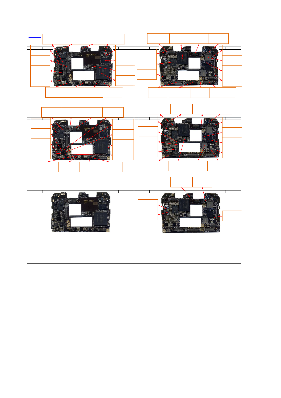
1. PCBA Components
Contents
2. PMU Output Voltages
3. No Current
4. Weak Current
5. Excessive Current
6. Power-on Sequence
7. Power-off Sequence
8. RF Transmission Framework
9. RF Reception Framework
10.GSM Transmission Failure(GSM_HB/GSM_LB)
11.GSM Reception Failure(GSM_LH/GSM_HB)
12.WCDMA Transmission Failure(B1/B2/B5/B8)
13.WCDMA Reception Failure(B1/B2/B5/B8)
14.TD_SCDMA Transmission Failure(B34/B39)
15.TD_SCDMA Reception Failure(B34/B39)
16.FDD_LTE Transmission Failure(B1/B2/B3/B5/B7/B8/B12/B17)
17.FDD_LTE Main Reception Failure(B1/B2/B3/B5/B7/B8/B12/B17)
18.FDD_LTE Diversity Reception Failure(B1/3)
19.FDD_LTE Diversity Reception Failure(B5/8)
20.TDD_LTE Transmission Failure(B38/B40/B41)
21.TDD_LTE Main Reception Failure(B38/B40/B41)
22.TDD_LTE Diversity Reception Failure(B38/B40/B41)
23.AFC Failure
24.WIFI&BT Failure
25.LCD Failure
26.Touch Failure
27.Rear Camera Failure 1
28.Rear Camera Failure 2
29.Rear Camera Failure 3
30.Rear Camera Failure 4
31.Front Camera Failure 1
32.Front Camera Failure 2
33.Camera Laser Failure
34.Primary SIM Card Detection Failure
35.Secondary SIM Card Detection Failure
36.SD Card Detection Failure
37.Charging Failure
38.USB Port Detection Failure
39.Speaker&Receiver Failure
40.Button Failure
41.Microphone Failure
42.Headset Failure
43.Gravity Sensor Failure
44.Proximity Sensor Failure
45.Flash Failure
46.GPS Failure
47.Motor Failure
48.Fingerprint Sensor Failure
49.Compass Failure
50.OTG Port Detection Failure
51.Barometer Failure
52.Infrared Failure
53.HALL Failure
54.NFC Failure
1. The tested values of resistance, impedance,
and diode in this guide are for your reference only.
2. The tested values vary by test equipment.
Compare the tested values to those of a good
PCBA when in use.
3. In this maintenance guide, the test voltage
mode is set to 5 V and the test resistance mode is
set to 2 W.
Notes
2019/3/26 第1页,共55页
Mate20 RS top(1).xlsx
Contents
U3301 RF transceiver
chip
Faulty symptom:
Signal failure
U2602 gravity sensor
1 TOP Side 1 BOTTOM Side
chip
Faulty symptom:
Gravity sensor failure
J2001 rear camera
connector 1
Faulty symptom:
Camera failure
U2201 Audio decoding
chip
Faulty symptom:
Audio failure
U1902 camera power
supply chip
Faulty symptom:
Camera/NFC/OTG failure
U2501 charging
management chip 2
Faulty symptom:
Charging or startup
failure
U2603 barometer
Faulty symptom:
Air pressure failure
2 TOP Side 2 BOTTOM Side
U3201 RF power supply
chip
Faulty symptom:
Signal failure
Q1612 MOS tube 4
Faulty symptom:
WIFI/BT failure
U1701 LCD display chip
Faulty symptom:
LCD failure
U1801 charging
management chip 3
Faulty symptom:
Charging failure
D2103 transient
suppression diode 2
Faulty symptom:
Charging failure
LED2701 infrared lamp
Faulty symptom:
Remote control
identification failure
U1603 charging
management chip 1
Faulty symptom:
Charging or startup
failure
X5701 27.4MHz crystal
oscillator
Faulty symptom:
NFC failure
U1802 wireless charging
management chip
Faulty symptom:
Charging failure
TCXO5101 38.4M clock
Faulty symptom:
WIFI failure
U2104 USB
conversion chip
Faulty symptom:
USB identification
failure
U5701 NFC chip
Faulty symptom:
NFC failure
D2109 transient
suppression diode 1
Faulty symptom:
Charging failure
U5501 RF switch
Faulty symptom:
WIFI/BT failure
J1901 rear camera
connector 2
Faulty symptom:
Camera failure
Q1604 MOS tube 1
Faulty symptom:
Charging failure
U2100 TYPEC conversion
switch
Faulty symptom:
TYPEC identification failure
PCBA Components
U5502 RF switch
Faulty symptom:
WIFI failure
U5100 WIFI/BT/GPS
chip
Faulty symptom:
WIFI/BT/GPS failure
U1201 BUCK BOOST
chip
Faulty symptom:
Startup failure
U300/U300_POP
CPU/DDR chip
Faulty symptom:
Startup or function failure
X1201 38.4M crystal
oscillator
Faulty symptom:
Startup failure
Q2502 MOS tube 2
Faulty symptom:
Charging failure
U1901 flash drive
Faulty symptom:
Flash failure
Q2501 MOS tube 3
Faulty symptom:
Charging failure
J5401 WIFI RF connector 1
Faulty symptom:
WIFI failure
J5601 WIFI RF
connector 2
Faulty symptom:
Signal failure
U1000 power
management chip
Faulty symptom:
Startup or function failure
U1302 GPU power
supply chip
Faulty symptom:
Startup failure
J1701 LCD/TP/
fingerprint connector
Faulty symptom:
Display/touch/fingerprint
failure
J1902 infrared connector
Faulty symptom:
Infrared identification failure
J5501 WIFIRF
connector 3
Faulty symptom:
Gravity sensor failure
U1702 LCD power
supply chip
Faulty symptom:
Display failure
U1703 fingerprint
power supply chip
Faulty symptom:
Fingerprint identification
failure
U1301 CPU power
supply chip
Faulty symptom:
Startup failure
J2803 flash connector
Faulty symptom:
Flash failure
U1400 UFS chip
Faulty symptom:
Startup failure
J2901 main FPC connector
Faulty symptom:
Charging/microphone/SD
card failure
MIC2301 secondary MIC
Faulty symptom:
Microphone failure
U6001 MIPI chip
Faulty symptom:
Signal failure
J2002 front camera
connector
Faulty symptom:
Camera failure
J1501 battary connector
Faulty symptom:
Startup/charging failure
J2003 IR supplement
light connector
Faulty symptom:
IR supplement
light failure
U3601 RF multifunctional chip
Faulty symptom:
Signal failure
J3801 diversity RF
connector
Faulty symptom:
Signal failure
J4401 MIMO RF
connector
Faulty symptom:
Signal failure
U3401 RF multifunctional component
Faulty symptom:
Signal failure
U3902 RF low noise
amplifier
Faulty symptom:
Signal failure
J3802 main RF
connector
Faulty symptom:
Signal failure
J2902 adapter board connector
Faulty symptom:
Speaker/receiver/power button
failure
U5904 RF switch
Faulty symptom:
Signal failure
U5903 RF switch
Faulty symptom:
Signal failure
U3701 RF PA
Faulty symptom:
Signal failure
U3501 RF multifunctional component
Faulty symptom:
Signal failure
J3804 coaxial cable
connector
Faulty symptom:
Signal failure
J2801 speaker/main MIC
connector
Faulty symptom:
Speaker/microphone failure
J2804 Tri-color indicator
connector
Faulty symptom:
Tri-color indicator failure
3 TOP Side 3 BOTTOM Side
U5401 RF switch
Faulty symptom:
WIFI failure
U5402 RF switch
Faulty symptom:
WIFI failure
J3803 diversity RF
connector
Faulty symptom:
Signal failure
U3803 RF switch
Faulty symptom:
Signal failure
2019/3/26 第2页,共55页

Contents
1
2
34
X1201
1 2
C1032
1.8V
Contents
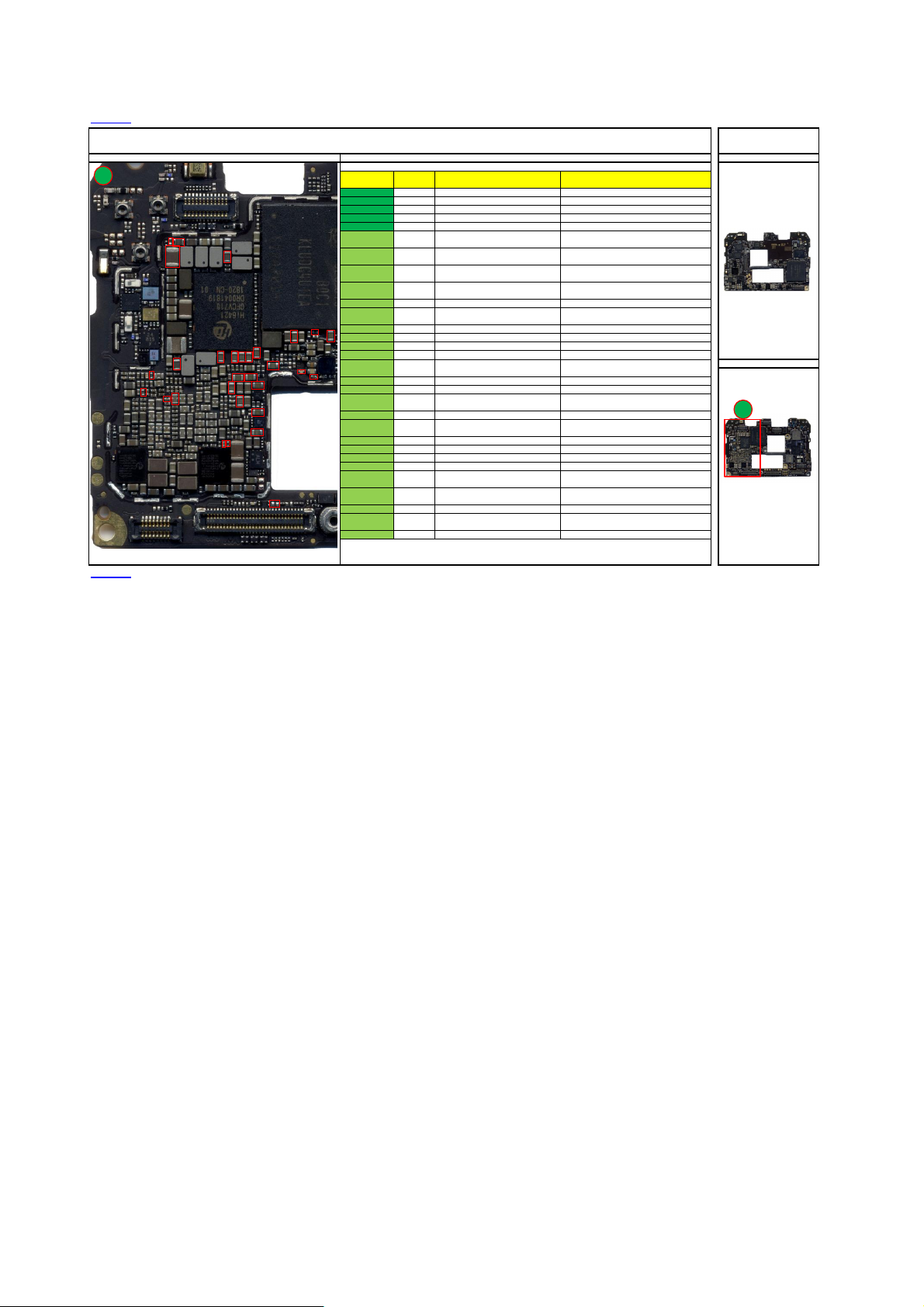
Mate20 RS top(1).xlsx
PMU Output Voltage Test Points and Voltage Values Panorama
Test Points PMU Output Voltage Test Points and Voltage Values TOP Side
C1101
C1060
1.8V
C1111
0.7V
C1116
3.8~4.2V
C1031
2.78V
C1150
C1156
0.8V
1.8V
0.9V
C1130
1.3V
C1146
1.95V
U1000
C1051
0.44V
C1028
1.7~或1.35V
C1053
C1056
0.8V
C1040
C1054
C1012
1.1V
1.85V
1.2V
C1144
1.3V
C422
1.12V
1.8~或2.95V
1V
C1007
C1009
1.29V
C1052
1.03V
0.9V
C1041
C1027
0.85V
1.2V
C1034
1.8V
C1022
0.8V
C1045
1.8V
C1020
3.3V
C1039
1.8~或2.95V
C473
C477
1.8~或2.95V
C1154
0.6V
C435
1.8V
C570
3.2V
C507
C572
0.8V
0.75V
U300
TP3083
1.8V
Voltage Name
VBUCK0_0V75
VBUCK1_1V12 1.12V after the ph one starts up U300; not powered off in standby
VBUCK2_1V3
VBUCK3_1V95
VBUCK4_0V7 0.7V after the pho ne starts up
VBUCK5_0V8 0.8V after the pho ne starts up
U1400
VBUCK6_0V7 0.7V after the pho ne starts up
VBUCK7_0V6 0. 6Vafter the phone starts up
VBUCK8_1V8
VBUCK9_0V9 0.9V after the pho ne starts up
VOUT_PMUD_1V8
VOUT9_SDIO_1V8/2
C1030
C1042
C1061
1.8V
2.5V
C1008
0.75V
C1050
0.75V
C1035
C1044
1.12V
C1014
1.85V
1.8V
3
VOUT11_USIM0_1V
2.85V
C1049
C1033
C1404
2.95V
1.8V
3.3V
C1036
3.9V
C1017
VOUT12_USIM1_1V
1.2V
C1018
2.9V
1.8或2.95V
VOUT14_2V85
C1047
C1062
1.8V
VOUT15_2V95 2.95V after the phone starts up U1400; not powered off in standby
VOUT16_1V8/2V95 2.95 V after the SD card i s installed J2901; powered off in stand by
VOUT17_TP_AVDD
VOUT23_3V2 3.2V after the phone starts up U300; powered off in standby
VOUT24_3V0 Actual 2.8V after the phon e starts up J2801; no t powered off in standby
VOUT27_1V8
VOUT34_3V3 3.3V after the phone starts up
TP3012
VOUT_PMUH_2V9 2.9V after the pho ne starts up U1000; powered off in stand by
3.8~4.2V
VOUT4_1V85_LCD_
C1740
1.8V
VOUT18_1V8 1.8V after the phone starts up U5100/U5701/U6001; not powered off in stan dby
VOUT21_CAM_IOV
VOUT26_1V7/1V35
VOUT28_1V8
VOUT29_TPIO_1V8
VOUT_PMUA_1V8
LDO_BUFF_1V8 Actual 3.9V after the phon e starts up U1000; not powered off in standby
VOUT0_0V75 0.75V after the phone starts up U300; not power ed off in standby
VOUT30_0V75 0.8V after the phone starts up U300; powered off in standby
VOUT39_0V8 0.8V after the phone starts up U300; powered off in standby
VOUT40_0V8 0.8V after the phone starts up U300; powered off in standby
VOUT1_1V09 1.09V after the RF is enabled U3301; powered off in standby
VOUT25_LCD_DIG_
VOUT32_CAM_DVD
VOUT37_1V2 after the phone starts u p1.2V U300; powered o ff in standby
VOUT38_TCAM_DV
VOUT41_1V2 1.2V after the phone starts up U2201; not powered off in standby
VOUT6_0V85 0.85V after the phone starts up U300; powered o ff in standby
VREF_COUL 1.29V after the phone star ts up Reference voltage; n ot powered off in standby
VREF_LDO_0V45 0.45V after the phone star ts up Reference voltage; n ot powered off in standby
VREF_LDO_0V9 0.9V after the phone star ts up Reference voltage; n ot powered off in standby
Test Point Status and Reference Value Ower Supplied to and Standby Status
3.8~4.2V when the phon e is powered on Battary
TP3012
VBATT
VBAT_SYS
VCOIN_2V5 Actual after the phone starts up3.31V U1000; not powered off in standby
V95
8/2V95
8/2V95
_3V3
VOUT2_1V8 1.8V after the phone starts up U300; powered off in standby
VOUT3_1V8
IO
VOUT5_1V8 1.8V after the front camera is started U300; powered off in standb y
VOUT7_1V8 1.8V after the phone starts up U300; powered off in standby
VOUT8_1V8 1.8V after the phone starts up U3901; not powered off in standby
DD_1V8
5
1V2
D_1V1
DD_1V
VREF 1.03V after the phone star ts up Reference voltage; n ot powered off in standby
VREF_RF 0.75V after the phone star ts up Reference voltage; n ot powered off in standby
3.8~4.2V when the phon e is powered on
C1116
C507
0.75V after the phone star ts up U300; powered off in standby
C422
1.3V after the phone star ts up
C1144
1.95V after the phone star ts up
C1146
C1148
C1150
L1111
C1154
1.8V after the phone star ts up
C1156
C1101
1.8V when the phone is powered on
C1035
C1061
C473
1.8 V after the SD card is installed U300; powered off in standby
Install the 3G card 1. 8V/install the 4G card
C477
C1062
C1030
C1404
C1039
C1020
C570
C1031
C1032
C1033
C1018
C1034
C1042
C1044
C435
C1045
C1047
C1014
C1060
C1028
C1049
C1740
TP3083
C1036
C1050
C1053
C572
C1022
C1040
C1054
C1056
C1041
C1012
C1017
C1027
C1007
C1008
C1009
C1051
C1052
2.95V
Install the 3G card 1. 8V/install the 4G card
2.95V
2.85V after the RF is en abled J2801/J2901/U3402; powered off in standby
3.3V connecting the L CD after
the phone starts up
1.8V after the phone star ts up
1.8V after the RF is en abled
1.8 V after connecting to the LCD J1701; powered off in standb y
1.8V after the RF is en abled
Actual 1.35V after the phon e starts up
1.8V after the RF is en abled
1.85V connecting the L CD after
the phone starts up
1.8V after the phone star ts up U1201; not powered off in standby
1.2V connecting the L CD after
the phone starts up
1.1V after the front cam era is started J1902; powered off in standby
1V after the front cam era is started J1901; powered off in standby
U1400/U1603/U300; not powered off in standby
U1704/J1701/U1703; not p owered off in standby
U3301/U3404/U3901; po wered off in standby
J2801/U3201/U3501; power ed off in standby
System
U1000; not powered off in standby
U1902/U2201; not po wered off in standby
U300; powered o ff in standby
U300; powered o ff in standby
U300; powered o ff in standby
U300; powered o ff in standby
U1000; not powered off in standby
U1000; not powered off in standby
U5701/U300; powered off in standby
U1000; powered o ff in standby
J1701; powered off in standby
X1201; not powered off in standby
J1901/J1902/J2001; powered o ff in standby
U1000; not powered off in standby
J1701; powered off in standby
J1701; powered off in standby
2
BOTTOM Side
1
3
2019/3/26 第3页,共55页

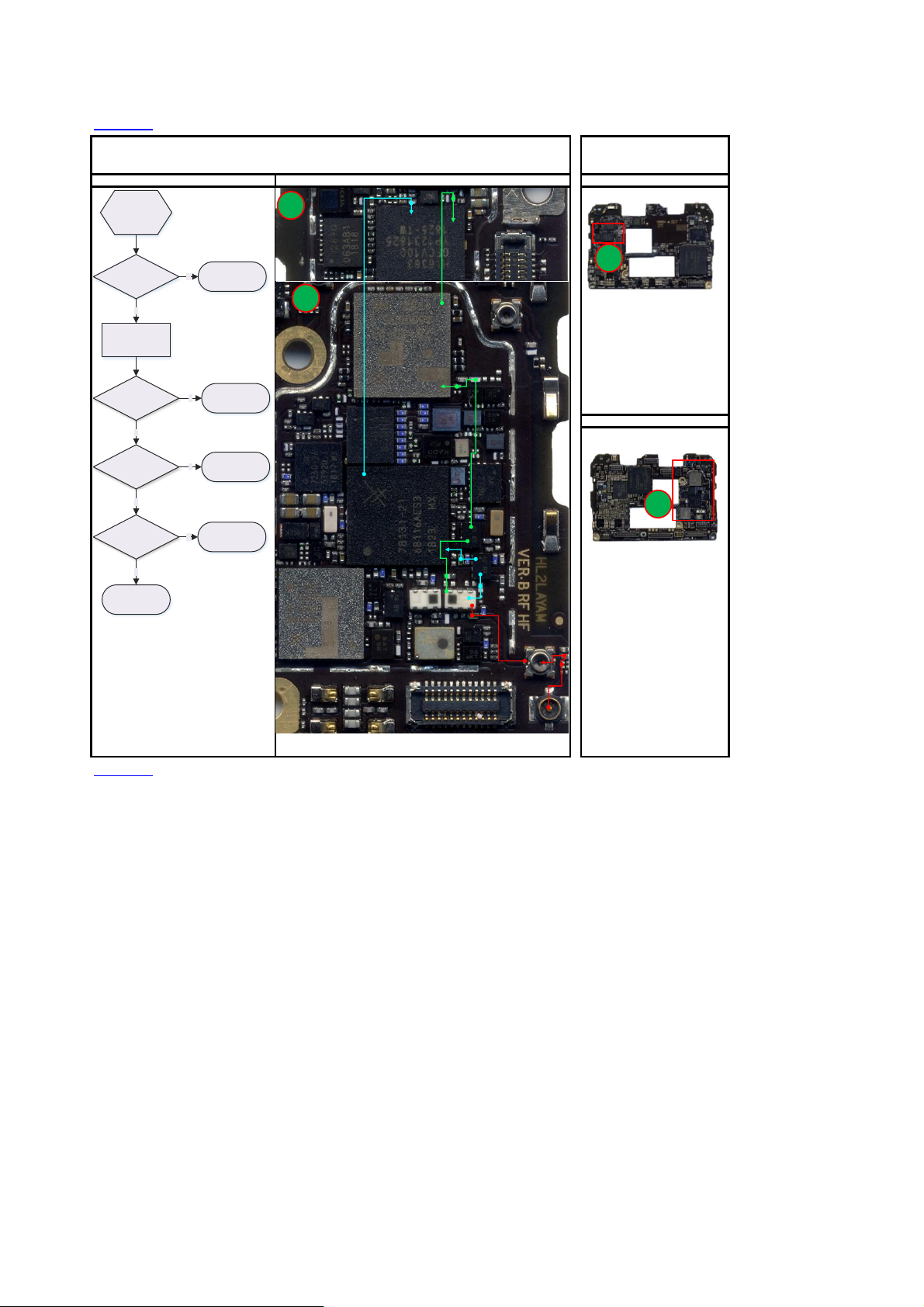
Contents
Replace U
1000.
Replace the defective
components.
If small components
are not damaged,
replace J
2902.
Is the appearance of
the PCBA normal?
4. Power on the
phone and
short-circuit
CHARGE
_PWRON_N
(J2902 PIN9) to the
ground. Is the startup
normal?
1
. Are the diode
values of
VBAT_SYS(C1116)
VBATT
(TP3012)
normal?
Check for defective
components on these
circuits.
Y
N
Startup
failure
(no current)
N
N
Y
2. Is the diode value
and voltage of
CHARGE_PWRON_N
(J2902 PIN9)
normal?
If small components
are not damaged,
replace U1000.
N
Y
3. Power on the
phone. Are the
voltages of
VBAT_SYS
(C1116)
VBATT(TP3012 )
normal?
Check for defective
components on these
circuits.
N
Y
Measure the power
-on
sequence (based on
the test points
). Is
there a short circuit
?
Rectify the fault
according to the
short circuit.
Y
N
Y
Maintenance Process
Mate20 RS top(1).xlsx
Startup Failure (No Current) Panorama
Test Points TOP Side
5
J2902
27
0.37V
U1400
0.46V
3.3V
6
33
0.33V
3.93V
0.28V
1.8V
1/3.TP3012
diode:0.49V
voltage:
3.8~4.2V
1
2
2
1.8V
3
0.45V
0.58V
0.39V
2.95V
38
36
31
9
0.21V
1.2V
0.44V
25
0.58V
BOTTOM Side
1
1
1/3.C1116
diode:0.34V
3.8~4.2V
0.37V
0.7V
2.63V
4
1.8V
voltage:
0.38V
1.8V
3
15
0.75V
0.62V
2.79V
0.35V
1.8V
29
0.3V
0.42V
0.7V
14
35
21
17
0.32V
0.8V
2/4.PIN9
diode:2.63V
voltage:1.8V
The phone can be
powered on after
be short-circuited
to the ground.
0.23V
0.6V
20
19
0.18V
1.12V
18
0.29V
1.8V
U1000
0.26V
1.3V
8
0.34V
0.85V
0.31V
0.32V
0.8V
1.2V
0.31V
1.2V
22
0.59V
3.2V
0.33V
0.75V
30
23
24
0.38V
1.8V
0.29V
11
0.9V
0.31V
7
1.95V
0.35V
10
1.35V
0.33V
16
13
0.75V
0.32V
26
34
1.8V
0.3V
28
1.2V
32
0.37V
1.8V
39
0.37V
1.8V
0.35V
12
1.8V
0.54V
1.8V
1
U300
0.45V
37
Contents
2019/3/26 第4页,共55页
0.91V
0.38V
1.8V
2

Contents
Startup
failure(weak
current)
Is the appearance of
the PCBA normal?
Replace the defective
components.
Measure the power-on
sequence (based on
the test points). Is
there a short circuit on
the PCBA?
1. Short-circuit
TP3018
to the ground
,
is a 1.0
displayed?
Repair the phone
based on the short
circuit maintenance
process.
2. Power on the
phone and press the
power button to
measure the clock.
Are X1201(PIN1/PIN3)
Waveform normal?
Replace X
1201 and
U1000 in sequence
.
Can the phone
be powered on after
software loading?
End
Replace U1400 and
U300
in sequence.
Are the voltages
required for the
startup normal
(based on the test
points)?
Check for defective
components on the
abnormal circuits
.
Replace
U1000 and U
300 in
sequence.
Y
N
N
Y
Y
N
N
Y
N
Y
Y
N
Mate20 RS top(1).xlsx
Startup Failure (Weak Current)
Input wave diagram PIN3 Output wave diagram PIN1
Panorama
Test PointsMaintenance Process
5
27
0.37V
1.8V
U1400
0.46V
0.39V
3.3V
2.95V
6
33
0.33V
3.93V
0.28V
25
1.8V
1.Short-circuit
TP3018 to the
ground,
1.0 port
is displayed.
31
0.21V
1.2V
0.45V
0.58V
9
0.44V
0.58V
38
36
1
0.29V
11
0.31V
1.2V
22
0.59V
3.2V
0.33V
0.75V
30
23
24
0.38V
1.8V
0.9V
0.31V
7
1.95V
0.35V
10
1.35V
0.33V
16
13
0.75V
0.32V
26
34
1.8V
0.3V
28
1.2V
32
0.37V
1.8V
18
17
0.32V
0.8V
0.23V
0.6V
20
19
0.18V
1.12V
0.29V
1.8V
U1000
0.26V
1.3V
8
0.34V
0.85V
0.32V
0.31V
1.2V
0.8V
0.3V
14
0.75V
0.62V
35
2.79V
0.42V
21
0.7V
0.35V
0.38V
1.8V
1.8V
29
3
0.37V
15
0.7V
2.63V
4
1.8V
TOP Side
2
BOTTOM Side
1
2
34
X1201
1 2
12
0.35V
1.8V
0.45V
37
0.91V
Contents
2019/3/26 第5页,共55页
39
0.37V
1.8V
U300
0.38V
1.8V
0.54V
1.8V
2
1

Contents
Power-on excessive
current
Startup excessive
current
Replace the damaged
components.
Press and hold the
power button and
observe the current. If
the current is greater
than 200 mA, the
related power supply
circuit is short-
circuited. Measure the
current based on the
power-on sequence.
Check for the short
circuit.
Check
VBAT/VBAT_SYS for
short circuits using the
temperature sensing or
ohm method.
Startup
failure
(excessive
current)
Maintenance Process
Mate20 RS top(1).xlsx
Startup Failure (Excessive Current) Panorama
Test Points TOP Side
1
0.29V
11
0.31V
22
1.2V
0.33V
0.75V
23
24
0.38V
1.8V
0.9V
0.31V
7
1.95V
0.35V
10
1.35V
0.33V
16
13
30
0.75V
0.32V
26
34
1.8V
0.3V
28
1.2V
0.37V
0.7V
0.38V
1.8V
18
17
0.32V
0.8V
0.23V
0.6V
20
19
0.18V
1.12V
0.29V
1.8V
U1000
0.26V
1.3V
8
0.34V
0.85V
0.31V
0.32V
0.8V
1.2V
0.3V
14
0.75V
0.62V
35
2.79V
0.42V
21
0.7V
0.35V
1.8V
29
3
15
U1400
0.46V
3.3V
6
33
0.33V
3.93V
0.28V
1.8V
5
0.37V
1.8V
25
0.39V
2.95V
31
0.21V
1.2V
0.45V
0.58V
9
0.44V
0.58V
2
BOTTOM Side
38
36
0.35V
1.8V
0.59V
32
3.2V
1
39
1.8V
U300
0.37V
1.8V
27
0.38V
1.8V
0.54V
1.8V
2
1
2.63V
4
1.8V
2
34
X1201
1 2
12
0.45V
37
0.91V
0.37V
Contents
2019/3/26 第6页,共55页

Contents
Contents
Power on sequence Signal Pin
PWR_HOLD 1 C 1202 0.54V 1.8V
SYS_RST_N 2 R1601 0.38V 1.8V
SOC_RST_PMU_N
(POR_RST)
PWRON_N 4 TP3035 2.63V 1.8V
VOUT_PMUA
(LDO_PMUA)
VOUT34_3V3
(LDO34)
VBUCK3_1V95
(BUCK3)
VBUCK2_1V3
(BUCK2)
VOUT41_1V2
(LDO41)
VOUT26_1V7/1V35
(LDO26)
VBUCK9_0V9
(BUCK9)
VOUT27_1V8
(LDO27)
VOUT0_0V75
(LDO0_1)
VBUCK0_0V75
(BUCK0)
VBUCK6_0V7
(BUCK6)
VOUT30_0V75
(LDO30)
VOUT39_0V8
(LDO39)
VBUCK8_1V8
(BUCK8)
VBUCK1_1V12
(BUCK1)
VBUCK7_0V6
(BUCK7)
VBUCK4_0V7
(BUCK4)
VOUT40_0V8
(LDO40)
VOUT6_0V85
(LDO6)
VOUT7_1V8
(LDO7)
VOUT8_1V8
(LDO8)
VOUT36_1V2
(LDO36)
VOUT29_TPIO_1V8
5(LDO29)
VOUT37_1V2
(LDO37)
VOUT5_1V8
(LDO5)
VOUT38_TCAM_DV
DD_1V2(LDO38)
VOUT15_2V95
(LDO23)
VOUT23_3V2
(LDO23)
LDO_BUFF_1V8
(LDO_BUF)
VOUT18_1V8
(LDO18)
VOUT24_3V0
(LDO24)
SYS_CLK
(SYS_CLK_38M4)
ABB_CLK_38M4 37 C1208 0.45V 0.91V
UFS_REF_CLK
(UFS_CLK_19M2)
SYS_CLK32_32K
(CLK32_SYS)
Mate20 RS top(1).xlsx
Location
Diode Voltage
number
3 C1205 0.38V 1.8V
5 TP3083 0.37V 1.8V
6 C1033 0.46V 3.3V
7 C1146 0.31V 1.95V
8 C1144 0.26V 1.3V
9 C1017 0.21V 1.2V
10 C1028 0.35V 1.35V
11 C1101 0.29V 0.9V
12 C1032 0.35V 1.8V
13 C1050 0.33V 0.75V
14 L1107 0.3V 0.75V
15 C480 0.37V 0.7V
16 C1053 0.33V 0.75V
17 C501 0.32V 0.8V
18 C1128 0.29V 1.8V
19 C422 0.18V 1.12V
20 C417 0.23V 0.6V
21 C1147 0.42V 0.7V
22 C1022 0.32V 0.8V
23 C1027 0.34V 0.85V
24 C1045 0.38V 1.8V
25 C1047 0.28V 1.8V
26 C1021 0.31V 1.2V
27 C1740 0.37V 1.8V
28 C1041 0.3V 1.2V
29 C435 0.35V 1.8V
30 C1012 0.31V 1.2V
31 C1413 0.39V 2.95V
32 R2101 0.59V 3.2V
33 C1036 0.33V Actual 3.93V
34 C1014 0.32V 1.8V
35 C1031 0.28V Actual 2.79V
36 R1218 0.44V 0.58V
38 R1228 0.45V 0.58V
39 R1219 0.37V 0.9V
Test Points
5
1
11
18
0.3V
0.75V
0.62V
2.79V
0.42V
0.7V
0.35V
0.38V
1.8V
1.8V
29
3
0.37V
15
0.7V
2.63V
4
1.8V
`
2
0.35V
12
1.8V
0.29V
14
1.8V
7
35
U1000
21
0.33V
10
0.75V
0.31V
16
0.26V
0.23V
30
1.2V
1.3V
0.6V
0.31V
26
20
1.2V
8
0.34V
28
19
23
0.85V
0.18V
22
1.12V
17
0.32V
24
0.8V
0.32V
0.38V
0.8V
1.8V
0.59V
32
3.2V
39
0.37V
1.8V
0.45V
37
0.91V
U300
0.37V
1.8V
0.29V
0.9V
0.31V
1.95V
U1400
0.45V
0.58V
0.46V
0.39V
3.3V
2.95V
6
0.35V
33
1.35V
13
34
0.3V
1.2V
31
0.33V
0.33V
3.93V
0.75V
0.21V
0.32V
1.2V
1.8V
0.37V
1.8V
0.44V
0.28V
25
0.58V
1.8V
27
0.54V
1.8V
0.38V
2
1.8V
Panorama
TOP Side
2
38
36
9
BOTTOM Side
1
1
2019/3/26 第7页,共55页
Contents
1
Mate20 RS top(1).xlsx
Power off sequence Panorama
Test Points Power off sequence TOP Side
Voltage Name
VBUCK0_0V75
VBUCK4_0V7 0.7V after the phone starts up
VBUCK5_0V8 0.7V after the phone starts up
VBUCK6_0V7 0.7V after the phone starts up
VBUCK7_0V6 0.6V after the phone starts up
U1400
VOUT9_SDIO_1V8/
VOUT11_USIM0_1
VOUT12_USIM1_1
C1150
C1060
0.8V
1.8V
C1111
0.7V
C1130
1.3V
VOUT14_2V85
U1000
C1042
1.8V
C1053
C1056
0.8V
C1040
C1054
C1012
1.1V
1.85V
1.2V
1.8~或2.95V
1V
C1044
1.85V
C1041
C1027
0.85V
1.2V
C1022
0.8V
C1045
1.8V
1.8~或2.95V
C473
C477
1.8~或2.95V
C1018
1.8~或2.95V
C1034
1.8V
C1020
3.3V
C1039
C1740
1.8V
C1154
0.6V
C435
1.8V
C570
3.2V
C507
C572
0.8V
0.75V
VOUT16_1V8/2V95 2.95V after the SD card is inserted J2901; powered off in standby
VOUT17_TP_AVD
VOUT23_3V2 3.2V after the phone starts up U300; powered off in standby
C1030
2.85V
C1049
VOUT_PMUH_2V9 2.9V after the phone starts up U1000; powered off in standby
1.8V
VOUT2_1V8 1.8V after the phone starts up U300; powered off in standby
VOUT3_1V8
VOUT4_1V85_LCD
2.9V
C1062
VOUT5_1V8 1.8V after the camera is enabled U300; powered off in standby
VOUT7_1V8 after the phone starts up1.8V U300; powered off in standby
VOUT21_CAM_IO
VOUT28_1V8
VOUT29_TPIO_1V
VOUT30_0V75 0.8V after the phone starts up U300; powered off in standby
VOUT39_0V8 0.8V after the phone starts up U300; powered off in standby
VOUT40_0V8 0.8V after the phone starts up U300; powered off in standby
VOUT1_1V09 1.09V after the RF is enabled U3301; powered off in standby
VOUT25_LCD_DIG
VOUT32_CAM_DV
VOUT37_1V2 1.2V after the phone starts up U300; powered off in standby
VOUT38_TCAM_D
VOUT6_0V85 0.85V after the phone starts up U300; powered off in standby
Test Point Status and Reference Value ower Supplied to and Standby Status
0.75V after the phone starts up U300; powered off in standby
1.8 V after the SD card is inserted U300; powered off in standby
Insert the 3G card 1.8V/insert the 4G card
2.95V
Insert the 3G card 1.8V/insert the 4G card
2.95V
U5701/U300; powered off in standby
2.85V after the RF is enabled J2801/J2901/U3402; powered off in standby
3.3V connecting the LCD after the phone
starts up
1.8V after the RF is enabled
U3301/U3404/U3901; powered off in standby
1.8V after connecting to the LCD J1701; powered off in standby
1.8V after the RF is enabled
1.85V connecting the LCD after the phone
starts up
1.2V connecting the LCD after the phone
starts up
J2801/U3201/U3501; powered off in standby
1.1V after the camera is enabled J1902; powered off in standby
1V after the camera is enabled J1901; powered off in standby
2V95
V8/2V95
V8/2V95
D_3V3
_IO
VDD_1V8
85
_1V2
DD_1V1
VDD_1V
C507
C1148
C1150
L1111
C1154
C473
C477
C1062
C1030
C1039
C1020
C570
C1018
C1034
C1042
C1044
C435
C1045
C1060 1.8V after the camera is enabled J1901/J1902/J2001; powered off in standby
C1049
C1740
C1053
C572
C1022
C1040
C1054
C1056
C1041
C1012
C1027
U300; powered off in standby
U300; powered off in standby
U300; powered off in standby
U300; powered off in standby
U1000; powered off in standby
J1701; powered off in standby
J1701; powered off in standby
J1701; powered off in standby
BOTTOM Side
1
Contents
2019/3/26 第8页,共55页

Contents
U3301
transceiver
chip
TX1_HB3_GHB
TX1_LB2_GLB
TX1_LB1_LB
TX2_HB2_HB
TX2_HB1_MB
Z3702
filter
U3701
2G PA
GSM_HB_TX_AUX8
GSM_LB_TX_
OUT
Mate20 RS top(1).xlsx
RF Transmission Framework
B38/B41_TRX
B7_TRX
U3601
RF multifunctional
component
B7/38/41_TRX
U3501
RF multifunctional
component
U3401
RF multifunctional
component
B1/3/7/32/38_
CA_TRX
B1/3_TRX
LB_TRX
Z3602
Duplexer
U3505
Switch
Z3500
filter
Z3501
filter
MHB_TRX
Z3603
filter
U3803
RF
switch
U3802
RF
switch
Z3803
filter
J3804
Coaxial cable
connector
J3802
RF
connector
MAIN_ANT
Contents
2019/3/26 第9页,共55页

Contents
J3804
coaxial cable
connector
J3802
mian RF
connector
MAIN_ANT
Z3803
filter
MHB_MAIN_ANT0
U3803
switch
Mate20 RS top(1).xlsx
RF Reception Framework
PRX_HB2_B2/3/9/34/39
PRX_HB1_RFIC2_B1/4/66
Z3604
filter
Z3603
filter
Z3602
filter
PRX_HB3_B1/4/66
U3601
RF multi-
functional
component
PRX_HB2_RFIC2_B7/38/40/4
PRX_B1/4/66
U3500
B40_TRX
B38/41_TRX
B7_TRX
switch
switch
switch
U3602
U3505
B40_TRX_IN
B38/41_TRX
B7_TRX
U3501
MHB_TRX
RF
RF multi-
functional
component
U3301
transceiver
chip
U4501
transceiver
chip
J5912
antenna spring
J3801
diversity RF
connector
J5912
antenna spring
J3803
diversity RF
connector
Contents
DIV_LB_ANT2
Z3802
filter
DIV_MHB_ANT1
LB_MAIN_ANT0
LB_DIV_ANT2
U3802
switch
U3802
switch
U3803
switch
RF
RF
RF
LB_TRX
LB_DRX
(B8/12/17/20/26)
DRX_MHB
(B1/2/3/7/34/39/40/41)
U3401
RF multi-
functional
component
U4001
Diversity
antenna
switch
B12/17_DRX
B26_DRX
B8_DRX
B20_DRX
B2/3/9_DRX
B34/39/41_DRX
B40_DRX
B1/3/7/B2/4/66_DRX
PRX_LB(GSM850/900)
Z4002
filter
Z4004
filter
Z4005
filter
Z4001
filter
Z4103
filter
Z4101
filter
Z4105
filter
B3/9/B2_DRX_LNA_IN
Z4102
filter
B1/4/B66_DRX_LNA_IN)
U3902
diversity
low noise
amplifier
DRX_HB4_B1/4/34/39/66
U3901
DRX_HB1_RFIC2_B1/4/66
RF switch
DRX_HB3_RFIC2_B40
DRX_HB2_RFIC2_B7/38/41
DRX_HB2_B2/3/9
DRX_LB1
DRX_LB2_Listening
U3301
transceiver
chip
U4501
transceiver
chip
U3301
transceiver
chip
2019/3/26 第10页,共55页

Contents
GSM
transmission
failure
Are the appearance of
related components
normal?
Replace the defective
components.
Simulate transmission
in non-signaling mode.
GSM_LB is used as an
example.
Use a spectrum
analyzer for the point
test. Is the signal
output from
U3301(L3301)
normal?
If related components
are normal, replace
U1000 and U3301.
in sequence.
Y
Replace U3301.
If related components
are normal, replace
U1000 and U3601 in
sequence.
N
N
Y
Use a spectrum
analyzer for the point
test. Is signal that pass
through U3701(L3702)
normal?
N
Y
1. Are the voltages
of VOUT1_1V09(C3304)
VOUT3_1V8(C3303)
VOUT2_1V8(C3315)
normal?
2. Is the voltage of
VOUT28_1V8(C3548)
normal?
N
Replace U3701.Y
Y
N
If related components
are normal, replace
U1000 and U3802.
in sequence.
Use a spectrum
analyzer for the point
test. Is signal that pass
through U3802(L3821)
normal?
N
Y
3. Is the voltage of
VOUT14_2V85 (C3807)
normal?
N
Replace U3802.Y
Replace J3802 and
U3301 in sequence.
Use a spectrum
analyzer for the point
test. Are signals that
pass through
Z3803(C3803)
J3802(C3811)
normal?
If related components
are normal, replace
Z3803 and J3802 in
sequence.
N
Y
Use a spectrum
analyzer for the point
test. Is signal that pass
through U3401(C3405)
normal?
If related components
are normal, replace
U3401.
Y
N
Mate20 RS top(1).xlsx
GSM Transmission Failure(GSM_HB/GSM_LB) Panorama
Maintenance Process Test Points TOP Side
1
GSM_HB_TX
1.C3315
voltage:1.8V
2
U3301
GSM_LB_TX
U3401
C3405
L3815
C3303
C3304
1.C3304/C3303
voltage:
1.09V/1.8V
1
L3702
L3301
U3701
Z3702
voltage:1.8V
U3501
2.C3548
3.C3807
voltage:2.85V
BOTTOM Side
2
U3802
U3803
L3821
Z3803
C3803
C3811
L3836
J3802
J3804
Contents
2019/3/26 第11页,共55页
Mate20 RS top(1).xlsx
GSM
reception
failure
Are the appearance of
related components
normal?
Replace the defective
components.
N
Simulate reception in
non-signaling mode.
GSM_LB is used as
an example.
Use a spectrum
analyzer for the point
test. Is signal that pass
through J3802(C3803)
normal?
Y
Y
If components on the
circuit are normal,
replace J3802.
N
Use a spectrum
analyzer for the point
test. Are signals that
pass through
Z3803(L3821)
U3802(L3815)
normal?
If components on the
circuit are normal,
replace Z3803 and
U3802 in sequence.
N
Use a spectrum
analyzer for the point
test. Is signal that
pass through
U3401(L3402)
normal?
Y
If components on the
circuit are normal,
replace U3401.
N
Replace J3802 and
U3301 in sequence.
Y
Contents
GSM Reception Failure(GSM_LH/GSM_HB) Panorama
Maintenance Process Test Points TOP Side
1
L3402
U3301
GSM_HB_PRX
2
U3401
L3815
GSM_LB_PRX
C3405
1
Contents
U3501
L3821
Z3803
U3802
C3803
U3803
J3802
BOTTOM Side
2
C3811
L3836
J3804
2019/3/26 第12页,共55页

Contents
WCDMA
transmission
failure
Are the appearance
of related
components
normal?
Replace the defective
components.
Simulate transmission
in non-signaling mode.
TX_B1 is used as an
example.
Use a spectrum
analyzer for the point
test. Is the signal
output from
U3301(L3503)
normal?
If related components
are normal, replace
U1000 and U3301 in
sequence.
N
Y
Replace U3301.
N
N
1. Are the
voltages of
VOUT1_1V09(C3304)
VOUT3_1V8(C3303)
VOUT8_1V8(C3315)
normal?
Use a spectrum
analyzer for the point
test. Is signal that
pass through
U3501(L3507)
amplified?
N
Y
If related components
are normal, replace
U3201, U1000 and
U3501 in sequence.
2. Are the voltages of
MHB_RF_VO0_WPA
(L3525)
VOUT28_1V8(C3548) )
normal?
Replace U3501.
N
Y
Y
Y
Replace U3501,Z3500
and U3501 in
sequence.
Use a spectrum
analyzer for the point
test. Is signal
that pass through
U3803(L3822)
normal?
N
Y
If related components
are normal, replace
Z3803 and J3802 in
sequence.
Use a spectrum
analyzer for the point
test. Are signals
that pass through
Z3803(C3803)
J3802(C3811)
normal?
N
Y
Replace J3802 and
U3301 in sequence.
If related components
are normal, replace
U1000 and U3803 in
sequence.
3. Is the voltage of
VOUT14_2V85 (C3807)
normal?
Replace U3803.
N
Y
Use a spectrum
analyzer for the point
test. Are the signals
output from
Z3501(C3532)
Z3500(L3500)
U3501(C3520)
normal?
N
Y
Mate20 RS top(1).xlsx
WCDMA Transmission Failure(B1/B2/B5/B8) Panorama
Maintenance Process Test Points TOP Side
1
L3503
1.C3315
voltage:1.8V
U3301
C330
C330
1.C3304/C3303
voltage:
1.09V/1.8V
1
2
WCDMA B1/B2 TX
U3401
WCDMA B5/B8 TX
Contents
2.L3525
voltage:8.87V
2.C3548
voltage:1.8V
U3501
WCDMA B1 TX
C3542
Z3500
L3500
Z3501
C3532
L3507
C3520
Z3803
U3802
U3803
L3822
C3803
RF public cable
3.C3807
voltage:2.85V
J3802
J3804
L3836
C3811
BOTTOM Side
2
2019/3/26 第13页,共55页

Contents
WCDMA
reception
failure
Are the appearance
of related components
normal?
Replace the defective
components.
Simulate reception in
non-signaling mode.
B5_PRX is used as an
example.
Use a spectrum
analyzer for the point
test. Is signal that pass
through J3802(C3803)
normal?
If components on the
circuit are normal,
replace J3802.
Use a spectrum
analyzer for the point
test. Is signal that pass
through Z3803(L3821)
U3802(L3815)
normal?
If the components on
the circuit are normal,
replace Z3803 and
U3802 in sequence.
Use a spectrum
analyzer for the point
test. Is signals that
pass through
U3401(L3402)
normal?
If the components on
the circuit are normal,
replace U3401.
Replace J3802 and
U3301 in sequence.
N
N
N
N
Y
Y
Y
Y
Mate20 RS top(1).xlsx
WCDMA Reception Failure(B1/B2/B5/B8)
Maintenance Process Test points TOP Side
1
U4501
B1_RFIC2_PRX
2
L3402
U3301
Panorama
1
2
U3500
B1_RFIC1_PRX
WCDMA_B1_PRX
3
U3401
WCDMA_B2_PRX
U3501
L3821
C3405
Z3803
L3815
WCDMA_B5/B8_PRX
BOTTOM Side
3
U3802
U3803
C3803
C3811
L3836
J3802
J3804
Contents
2019/3/26 第14页,共55页

Contents
TD_SCDMA
transmission
failure
Are the appearance of
related components
normal?
Replace the defective
components
.
Simulate transmission
in non-signaling mode.
TX_B34 is used as an
example.
Use a spectrum
analyzer for the point
test. Is the signal
output from
U3301(L3503)
normal?
If related components
are normal
, replace
U1000 and U3301 in
sequence.
N
Y
Y
Replace U3301.
N
N
Y
1. Are the voltages of
VOUT1_1V09
(C3304)
VOUT
3_1V8(C3303)
VOUT8_1V8(C3315)
norma
l?
N
Y
Use a spectrum
analyzer for the point
test. Is the signal
output from
U3501(C3520)
normal?
N
Y
If related components
are normal, replace
U3201, U1000 and
U3501
in sequence.
2. Are the voltages
of MHB_RF_VO0_WPA
(L3525)
VOUT28_1V8(C3548)
normal?
Replace U3501.
N
Y
Use a spectrum
analyzer for the point
test. Are signals
that pass through
Z3803(C3803
)
J3802(
C3811)
normal?
N
Y
Replace J3802 and
U3301 in sequence
.
If related components
are normal, replace
U1000 and U3803 in
sequence.
3. Is the voltage of
VOUT14_2V85 (C3807)
normal?
Replace U3803.
N
Y
If related components
are normal, replace
Z3803 and J3802 in
sequence.
Use a spectrum
analyzer for the point
test. Is the signal
output from
U3803(L3822)
normal?
Mate20 RS top(1).xlsx
TD_SCDMA Transmission Failure(B34/B39) Panorama
Maintenance Process Test Points TOP Side
1
1.C3315
voltage:1.8V
L3503
U3301
B34/B39_TX
C3303
C3304
1.C3304/C3303
voltage:
1.09V/1.8V
1
2
2.C3548
voltage:1.8V
2.L3525
voltage:8.87V
U3501
C3520
Z3803
C3803
U3803
L3822
3.C3807
voltage:2.85V
J3802
C3811
L3836
BOTTOM Side
2
J3804
Contents
2019/3/26 第15页,共55页

Contents
TD-SCDMA
reception
failure
Are the appearance
of related components
normal?
Replace the defective
components.
Simulate reception in
non-signaling mode.
B34_PRX is use
d as an
example.
Use a spectrum
analyzer for the point
test
. Is signal that pass
through J3802(C3803)
normal?
If components on the
circuit are normal
,
replace J3802.
Use a spectrum
analyzer for the point
test. Are signals that
pass through
Z3803(L3822
)
U3803
(C3520)
normal?
If the components on
the circuit are normal,
replace Z3803
and
U3803 in sequence.
Use a spectrum
analyzer for the point
test. Is signal that pass
through U3501(L3511)
normal?
If the components on
the circuit are normal,
replace U3501.
Replace J
3802 and
U3301 in sequence.
N
N
N
N
Y
Y
Y
Y
Mate20 RS top(1).xlsx
TD_SCDMA Reception Failure(B34/B39)
Panorama
Maintenance Process Test Points TOP Side
1
L3511
1
B34/B39_RX
U3301
2
BOTTOM Side
U3501
2
C3520
U3803
L3822
Z3803
C3803
C3811
J3802
L3836
Contents
J3804
2019/3/26 第16页,共55页

Contents
FDD-LTE
transmission
failure
Are the appearance of
related components
normal?
Replace the defective
components.
Simulate transmission
in non-signaling mode.
TX_B1 is used as an
example.
Use a spectrum
analyzer for the point
test. Is the signal
output from
U3301(L3503)
normal?
If related components
are normal
, replace
U1000 and U3301 in
sequence
.
N
Y
Y
Replace U3301.
N
N
Y
1. Are the voltages of
VOUT1_1V09(C3304)
VOUT3_1V8(C3303)
VOUT
8_1V8(C3315)
normal?
Use a spectrum
analyzer for the point
test. Is the signal
output from
U3501(L3507)
normal?
N
Y
If related components
are normal, replace
U3201, U1000 and
U3501 in sequence.
2. Are the voltages
of MHB_RF_VO0_WPA
(L3525)
VOUT28_1V8(C3548)
normal?
Replace U
3501.
N
Y
Use a spectrum
analyzer for the point
test. Is signal
that pass through
U3803(L3822)
normal?
N
Y
Y
Use a spectrum
analyzer for the point
test. Are signals
that pass through
Z3803(C3803)
J3802(C3811)
normal?
N
Y
Replace J3802 and
U3301 in sequence.
If related components
are normal, replace
U1000 and U3803 in
sequence.
3. Is the voltage of
VOUT
14_2V85 (C3807
)
normal?
Replace U3803.
N
Y
If related components
are normal, replace
Z3803 and J3802 in
sequence.
Use a spectrum
analyzer for the point
test. Are the signasl
output from
Z3501
(C3532)
Z3500(L3500)
U3501(C3520)
normal?
N
Replace Z3501, Z3500,
and U3501 in
sequence
.
Mate20 RS top(1).xlsx
FDD_LTE Transmission Failure(B1/B2/B3/B5/B7/B8/B12/B17) Panorama
Maintenance Process Test Points TOP Side
1
2
B7_TX
L3503
1.C3315
voltage:1.8V
U3301
1.C3304/C3303
voltage:
1.09V/1.8V
1
Contents
U3601
voltage:10V
2.L3525
U3401
U3501
B1/2/3_TX
B1/2/3/7_TX
L3500
U3505
Z3602
C3542
2.C3548
voltage:1.8V
L3507
Z3500
Z3501
U3802
Z3803
C3532
B5/8/12/17_TX
3.C3807
voltage:2.85V
U3803
RF public cable
J3803
J3804
L3836
C3811
BOTTOM Side
2
2019/3/26 第17页,共55页
 Loading...