

Page 1
COMPANY CONFIDENTIAL
SDR845 Gigabit RF Card
Engineering Requirements Specification
Project code: T77W980T00
Solution: SDR845
Copyright © 2017. Foxconn Communications Inc. All rights reserved.
- 1 -
Page 2
COMPANY CONFIDENTIAL
Department
Name
Signature
Review Dates
* Plan
** Results
Project Manager
Choro Chung
ProjectLeader
Jeff Guo
Hardware Engineer
Neil Li
Rev
Date
Originator
Comment
V1.0
2018/01/11
Neil Li
Initial release for carrier engagement, will update it after fix
hardware design
V1.1
2018/02/03
Neil Li
Update the mechanical drawing
V1.2
2018/02/06
Neil Li
Update the soldering condition
V1.3
2018/02/22
Neil Li
Update the soldering information
V1.4
2018/04/14
Neil Li
Update the Qlink information
V1.5
2018/05/22
Neil Li
Add the Qlink length information
V1.6
2018/06/13
Neil Li
Add the label information
Reviewers
Modification History
- 2 -
Page 3

COMPANY CONFIDENTIAL
CONTENTS
1. GENERAL DESCRIPTION........................................................................ 5
1.1 SYSTEM MAIN FEATURE ...................................................................... 6
1.2 CARRIER AGGREGATION COMBINATION ..................................... 8
1.3 SYSTEM BLOCK DIAGRAM .................................................................. 8
1.4 PIN DEFINITION ...................................................................................... 8
1.5 PLATFORM CONNECTION DESIGN ................................................. 13
2. HARDWARE FEATURES ........................................................................ 15
2.1 RF TRANSCEIVER ................................................................................. 15
2.2 ANTENNA DESIGN ................................................................................ 16
4.1RECOMMENDED OPERATING CONDITIONS ................................ 17
4.2 STORAGE REQUIREMENT ................................................................. 17
4.3 THERMAL DISSIPATION PROPOSAL .............................................. 17
4.4CRYSTAL MATERIAL ........................................................................... 17
4.5ELECTROSTATIC DISCHARGE .......................................................... 18
5. MECHANICS, MOUNTING AND PACKAGING ................................. 19
5.1MECHANICS ............................................................................................. 19
5.2MOUNTING ONTO THE APPLICATION PLATFORM ................... 22
5.2.1SMT PCB ASSEMBLY .......................................................................... 22
5.2.1.1LAND PATTERN AND STENCIL .................................................... 22
5.2.1.2BOARD LEVEL CHARACTERIZATION ...................................... 23
5.2.2MOISTURE SENSITIVITY LEVEL ................................................... 23
5.2.3SOLDERING CONDITIONS AND TEMPERATURE ...................... 24
5.2.3.1REFLOW PROFILE ........................................................................... 24
5.2.3.2MAXIMUM TEMPERATURE AND DURATION ......................... 25
5.2.4DURABILITY AND MECHANICAL HANDLING ........................... 25
5.2.4.1STORAGE LIFE .................................................................................. 25
5.2.4.2PROCESSING LIFE ........................................................................... 25
- 3 -
Page 4

COMPANY CONFIDENTIAL
5.2.4.3 BAKING .............................................................................................. 25
5.2.4.4 ELECTROSTATIC DISCHARGE ................................................... 26
5.3PACKAGING ............................................................................................. 26
5.3.1TAPE AND REEL .................................................................................. 26
5.3.1.1 ORIENTATION .................................................................................. 26
5.3.1.2BARCODE LABEL ............................................................................. 26
5.3.2SHIPPING MATERIALS ...................................................................... 26
5.3.2.1MOISTURE BARRIER BAG ............................................................. 27
5.3.2.2TRANSPORTATION BOX ................................................................ 27
6. SAMPLE APPLICATION ......................................................................... 28
- 4 -
Page 5
COMPANY CONFIDENTIAL
5
Form Fact
LGA 31x31 Module
Carrier Support
North America: AT&T, Verizon, T-Mobile, Sprint, Bell, Rogers
Europe: Vodafone, EE, DT, H3G, Orange, TEF, TIM, Swisscom
Russia: MTS
China: CMCC, CT, CU
Australia: Telstra, Optus
South Korea: SKT
Japan: KDDI, DCM, SBM
Carriers above is subject to biz discussion
QCT Solution
SDR845
LTE
Mode
FDD / TDD
Band
LB:B8/12(17)/13/14/20/26(5/18/19)/28/29 /B71
MB:B1/2(25)/3/4(66)/32/B39/B34
HB:B7/30/40/41(38)
3.5G:B42/43/48
LAA/LTE-U (DL only): B46
CA
5xDL CA (Up to 100MHz, 256QAM)
2xUL CA (Up to 40MHz. 64QAM) -- intra-band contiguous CA
MIMO
4X4(band plan: B1/2(25)/3/4(66)/7/30/40/41(38)/, 4X2, 2X2
Cat
(DL/UL Mbps)
ue-CategoryUL 13 (UL: 150Mbps) + ue-CategoryDL 16 (DL: 1.0Gbps) @ 2X2
ue-CategoryUL 13 (UL: 150Mbps) + ue-CategoryDL 18 (DL: 1.2Gbps) @ 4X4
3G
WCDMA
HSPA+ Rel8 (DL/UL: up to 42/11 Mbps)
Band
Band1/2/4/5(6/19)/8/9
GNSS
GPS/GLONASS/Beidou/Galileo
Interface
Qlink/MIPI/GRFC
1. General Description
T77W980T00 is designed to enable wireless data connectivity for notebook computer or any other
device which runs on Qualcomm Snapdragon SDM845/ SDM850, it is compatible with the LGA
interface 31x31type. It delivers wireless wide-area network (WWAN) connectivity for the LTE,
UMTS and GPS/GLONASS/Beidou/Galileo protocols in one hardware configuration.
Page 6
6
Feature
Description
Physical
LTE module, 31 x 31 mm, 183 pin LGA
Electrical
No single voltage supply
Dimension
Dimensions (L × W × H): 31 mm × 31 mm × 2.05 mm
Shielding design
Shield case on board design, no additional shielding requirement
Weight
4.4g
USIM
Off-board USIM connector supported
Operating Bands
WCDMA/HSDPA/HSUPA/HSPA+ operating bands:
Band 2: 1850 to 1910 MHz (UL), 1930 to 1990 MHz (DL)
Band 4: 1710 to 1755 MHz (UL), 2110 to 2155 MHz (DL)
Band 5: 824 to 849 MHz (UL), 869 to 894 MHz (DL)
LTE bands:
Band 2: 1850 to 1910 MHz (UL), 1930 to 1990 MHz (DL)
Band 4: 1710 to 1755 MHz (UL), 2110 to 2155 MHz (DL)
Band 5: 824 to 849 MHz (UL), 869 to 894 MHz (DL)
Band 7: 2500 to 2570 MHz (UL), 2620 to 2690 MHz (DL)
Band 12: 699 to 716 MHz (UL), 729 to 746 MHz (DL)
Band 13: 777 to 787 MHz (UL), 746 to 756 MHz (DL)
Band 14: 788 to 798 MHz (UL), 758 to 768 MHz (DL)
Band 17: 704 to 716 MHz (UL), 734 to 746 MHz (DL)
Band 25: 1850 to 1915 MHz (UL), 1930 to 1995 MHz (DL))
Band 26: 814 to 849 MHz (UL), 859 to 894 MHz (DL)
Band 29: 717 to 728 MHz (DL)
Band 30: 2305 to 2315 MHz (UL) 2350 to 2360 MHz (DL)
Band 38: 2570 to 2620 MHz (UL/DL)
Band 41: 2496 to 2690 MHz (UL/DL)
Band 66: 1710 to 1800 MHz (UL), 2110 to 2200 MHz (DL)
Band 71:663 to 698 MHz (UL), 617 to 652 MHz (DL)
Diversity/2nd Rx
All UMTS operating bands
All LTE operating bands
GNSS
GPS: L1 (1575.42MHz)
GLONASS: L1 (1602MHz)
Beidou (1561.098MHz)
Galileo (1575.42MHz)
Antenna connectors
MAIN and AUX(supports Diversity and GPS simultaneously)
Throughput
WCDMA CS: DL 64 kbps /UL 64 kbps
WCDMA PS: DL 384 kbps /UL 384 kbps
1.1 System Main Feature
COMPANY CONFIDENTIAL
Page 7

COMPANY CONFIDENTIAL
7
HSPA+:DL 21.6 Mbps /UL 5.76 Mbps
DC-HSPA+: DL 42 Mbps/UL 5.76 Mbps
LTE Cat4: DL:150 Mbps/UL 50 Mbps
LTE Cat6: DL:300 Mbps/UL 50 Mbps
LTE Cat9: DL:450 Mbps/UL 50 Mbps
LTE Cat11: DL:585 Mbps/UL 50 Mbps
LTE Cat16: DL:1Gbps/UL 150Mbps
LTE Cat18: DL:1.2Gbps/UL 150Mbps
LTE air interface
LTE Rel13
DL – 1.2 Gbps / 12-layer / 100 MHz CA
UL - 150 Mbps / 40 MHz CA
256 QAM DL / 64 QAM UL
4 × 2 MIMO 5x CA (R13)
4 × 4 MIMO 3x CA
FDD + TDD CA
3.5 GHz and 600 MHz Bands
LAA and LTE-U (up to 80 MHz of unlicens)
Advance LTE IC + NAIC (with CRS only)
WCDMA/HSPA air interface
R99:
All modes and data rates for WCDMA FDD
R5 HSDPA
PS data speeds up to 7.2 Mbps on the downlink
R6 HSUPA
E-DCH data rates of up to 5.76 Mbps for 2 ms TTI (UE category 6) uplink
R7 HSPA+
Downlink 64 QAM SISO: up to 21 Mbps
Downlink 16 QAM 2X2 MIMO: up to 28 Mbps
Uplink 16 QAM: up to 5.76 Mbps
R8 DC-HSPA+
Downlink dual carrier with 64 QAM (SISO); up to 42 Mbps
GNSS
Customizable tracking session
• Automatic tracking session on startup
• Concurrent standalone GPS, GLONASS, Beidou and Galileo
Page 8

COMPANY CONFIDENTIAL
8
• gpsOneXTRA with GPS + GLONASS + Beidou + Galileo support
1.2 Carrier aggregation combination
1.2.1. Refer to Qualcomm documents 80-P8641-123 Rev. A, Published: 2017/7/31.
Remark: T77W980 hardware design can support follow CA combination, but the Final CA
combinations plan depends on carrier engagement and Qualcomm software design.
1.2.2. Qualcomm SDX20 support 5CA+256QAM (up to Cat18) and Rel13 (FDD+TDD CA)
which is mandatory for AU/JP/China carriers.
Update the Carrier CA combination, please refer the document:
SDR845_CA_list_20180508 .xlsx
1.3 System Block Diagram
1. GRC is the RF only module, it doesn’t include the CPU & memory. So GRC doesn’t have the SW
image.
2. Each GRC will have its unique QCN data, it will use the GRC SN to name it, and provide these
data to one ftp server. OEM can scan the SN to get the QCN data then load it to the platform memory.
1. Just one antenna to support Tx;
2.Support 2 or 4 antennas simultaneously (2 ANTs up to Cat16: 2X2 MIMO+5CA, 4 ANTs up to
Cat18: 4X4 MIMO+3CA and 2X2 MIMO+5CA)
1.Single main antenna design with Pentaplexer;
2.All the PAMiD with PA+SW+Filter+LNA+ASM.
Figure 1-3-2 RF Block Diagram-DRX
1.Single aux antenna design with Pentaplexer;
2.Add QLN2042 for 3.5GHz
1.4 Pin definition
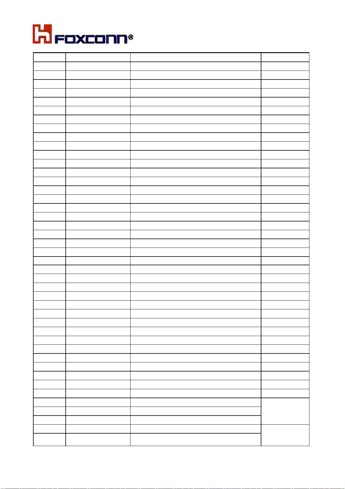
1.4.1 LGA interface Pin sequence
1.4.2 Pin definition
Table 1-4-2Definitions of pins on the LGA interface
Page 9
COMPANY CONFIDENTIAL
9
PIN #
Signal Name^
Description
Comments
A3
GND
GND
A4
GND
GND
A5
GND
GND
A6
GND
GND
A7
GND
GND
A8
GND
GND
A9
GND
GND
A10
GND
GND
A11
GND
GND
A12
GND
GND
B3
GND
GND
B4
GND
GND
B5
GND
GND
B6
GND
GND
B7
GND
GND
B8
GND
GND
B9
GND
GND
B10
GND
GND
B11
GND
GND
B12
GND
GND
B13
GND
GND
C1
GND
GND
C2
GND
GND
C3
GND
GND
C4
GND
GND
C5
GND
GND
C6
GND
GND
C7
GND
GND
C8
GND
GND
C9
GND
GND
C10
GND
GND
C11
GND
GND
C12
GND
GND
C13
GND
GND
C14
GND
GND
D1
GND
GND
D2
GNSS_EN
GNSS Enable
D3
GRFC4
Generic RF control
D4
VREG_L12M_2P7
Power supply input
For switch, for
FEM VDD
D5
VREG_L12M_2P7
Power supply input
D6
VREG_L12M_2P7
Power supply input
D7
VREG_L6M_1P8
VDD_1P8_DIG
For PA ,LNA,
FEM VIO,for
SDR845
D8
VREG_L6M_1P8
VDD_1P8_DIG
Page 10
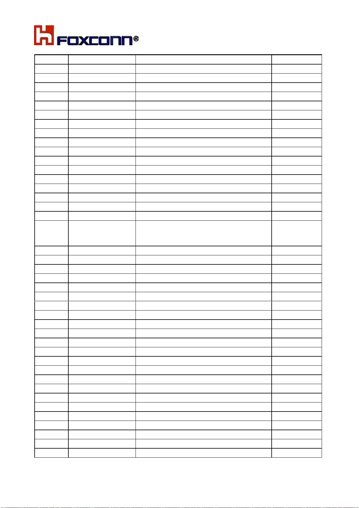
COMPANY CONFIDENTIAL
10
PIN #
Signal Name^
Description
Comments
1P8_DIG, for ET
D9
GRFC2
Generic RF control
D10
GND
GND
D11
GND
GND
D12
GND
GND
D13
GND
GND
D14
GND
GND
E1
GND
GND
E2
GND
GND
E3
GPIO_1
HW Version check
E4
GPIO_2
HW Version check
E5
GRFC6
Generic RF control
E6
GND
GND
E7
GND
GND
E8
GRFC7
Generic RF control
E9
GND
GND
E10
GND
GND
E11
PA_THERM_2
AMUX input for 3.5G PA thermistor
It is a NTC --
100Kohm 1%
170mW
E12
GND
GND
E13
GND
GND
E14
GND
GND
F1
GND
GND
F2
GND
GND
F3
RFFE3_DATA
MIPI RFFE data
F4
RFFE3_CLK
MIPI RF front end (RFFE) clock
F5
GND
GND
F6
RFFE4_CLK
MIPI RF front end (RFFE) clock
F7
RFFE4_DATA
MIPI RFFE data
F8
GND
GND
F9
RFFE6_CLK
MIPI RF front end (RFFE) clock
F10
GND
GND
F11
GND
GND
F12
GND
GND
F13
GND
GND
F14
GND
GND
G1
GND
GND
G2
GND
GND
G3
GND
GND
G4
GND
GND
G5
GND
GND
G6
GND
GND
Page 11

COMPANY CONFIDENTIAL
11
PIN #
Signal Name^
Description
Comments
G7
GND
GND
G8
GND
GND
G9
RFFE6_DATA
MIPI RFFE data
G10
GND
GND
G11
GRFC1
Generic RF control
G12
GND
GND
G13
VREG_L5M
VDD_1P8_ANA_W0
G14
GND
GND
H1
GND
GND
H2
VREG_L6M_1P8
VDD_1P8_DIG
H3
VREG_L6M_1P8
VDD_1P8_DIG
H4
GND
GND
H5
QLINK_REQ
QLink request from SDR845
H6
QPHY_DL2_P
QLink downlink lane 2 – plus
H7
QPHY_DL1_P
QLink downlink lane 1 – plus
H8
GND
GND
H9
GND
GND
H10
GRFC3
Generic RF control
H11
VREG_L1M
VDD_1P2_ANA_W0
H12
VREG_L1M
VDD_1P2_ANA_W0
H13
VREG_L5M
VDD_1P8_ANA_W0
H14
GND
GND
I1
GND
GND
I2
VREG_L5M
VDD_1P8_ANA_W0
I3
VREG_L5M
VDD_1P8_ANA_W0
I4
GND
GND
I5
QLINK_EN
QLink Enable for SDR845
I6
QPHY_DL2_M
QLink downlink lane 2 – minus
I7
QPHY_DL1_M
QLink downlink lane 1 – minus
I8
GND
GND
I9
RFFE5_CLK
MIPI RF front end (RFFE) clock
I10
GND
GND
I11
PA_THERM_1
AMUX input for M/HB PA thermistor
It is a NTC --
100Kohm 1%
170mW
I12
VREG_L1M
VDD_1P2_ANA_W0
I13
VREG_L5M
VDD_1P8_ANA_W0
I14
GND
GND
J1
GND
GND
J2
VREF_DAC
Transmitter DAC voltage reference
J3
VREF_DAC
Transmitter DAC voltage reference
J4
GND
GND
J5
QPHY_DL0_P
QLink downlink lane 0 – plus
Page 12

COMPANY CONFIDENTIAL
12
PIN #
Signal Name^
Description
Comments
J6
QPHY_CLK_M
QLink clock – minus
J7
QPHY_UL0_P
QLink uplink lane 0 – plus
J8
GND
GND
J9
RFFE5_DATA
MIPI RFFE data
J10
GND
GND
J11
VREG_L8M
VDD_1P0_DIG_W0
For SDR845
J12
VREG_L6M_1P8
VDD_1P8_DIG
J13
GND
GND
J14
GND
GND
K1
GND
GND
K2
WMSS_RESET
Reset functionality for the digital sections
inside the transceiver
K3
VREF_DAC
Transmitter DAC voltage reference
K4
GND
GND
K5
QPHY_DL0_M
QLink downlink lane 0 – minus
K6
QPHY_CLK_P
QLink clock – plus
K7
QPHY_UL0_M
QLink uplink lane 0 – minus
K8
GND
GND
K9
GND
GND
K10
VREG_L8M
VDD_1P0_DIG_W0
K11
VREG_L8M
VDD_1P0_DIG_W0
K12
VREG_L6M_1P8
VDD_1P8_DIG
K13
VPH_QFE
Power supply input for RF
K14
GND
GND
L1
GND
GND
L2
GND
GND
L3
GRFC5
Generic RF control
L4
GND
GND
L5
GND
GND
L6
GND
GND
L7
GND
GND
L8
GND
GND
L9
GND
GND
L10
VREG_L3M
VDD_1P0_ANA_W0
For SDR845
L11
VREG_L6M_1P8
VDD_1P8_DIG
L12
VPH_QFE
Power supply input for RF -- 3.3V~4.4V
L13
VPH_QFE
Power supply input for RF -- 3.3V~4.4V
L14
GND
GND
M2
GND
GND
M3
GND
GND
M4
RF_CLK1
38.4 MHz reference input forPLLs and other
circuits
M5
GND
GND
Page 13

COMPANY CONFIDENTIAL
13
PIN #
Signal Name^
Description
Comments
M6
RFFE1_CLK
MIPI RF front end (RFFE) clock
M7
RFFE1_DATA
MIPI RFFE data
M8
GND
GND
M9
VREG_L3M
VDD_1P0_ANA_W0
M10
VREG_L3M
VDD_1P0_ANA_W0
M11
VPH_QFE
Power supply input for RF -- 3.3V~4.4V
M12
VPH_QFE
Power supply input for RF -- 3.3V~4.4V
M13
GND
GND
N3
GND
GND
N4
GND
GND
N5
GND
GND
N6
GND
GND
N7
GND
GND
N8
GND
GND
N9
GND
GND
N10
GND
GND
N11
GND
GND
N12
GND
GND
Metrics
Guidance
Comments
Total channel bus length
<=60mm
Maximun PCB bus routing length for entire ch
annel between SDM845 to GRC
Impedance
Diff Z0 min/max
Field route
85Ω +/- 10Ω
Differential PCB routing Z0
Length Match
Intrapair match
0.7mm
Length match between P and N side of differe
ntial pair, need to include the GRC internal
trace length
1.5 Platform connection design
1.5.1 For signal line impedance control
For Qlink signal line:
For Qlink line, shall shielding well for themself, difference control for each pair lines.
Please refer Qualcomm document: 80-P6348-3 Rev. A
1.5.2 For GRC mother board layout suggestion
a: Please put the Q-link signals routing on the first priority, Q-link signal frequency will be up to
6GHz. If GRC module mounts on the mother board top side, that on the mother board PCB top layer,
please don’t have the other signal trace during the position of these Q-link signals. Detail location
please see the below pictures.
Page 14

COMPANY CONFIDENTIAL
14
b: For Q-link signal lines’ upper and lower layers must be GND, they should be wrapped up in GND
well. GRC also have the MIPI line, suggest to route by differential.
If GRC module mounts on the mother board top side, please reserve the relative position clearance
on the back side. We need to consider the thermal, reserve the location for future thermal solution. So
it is better that don’t put the components on the GRC module back side.
Please refer the below picture, suggest to reserve the red dotted line location (31L * 25H mm).
Figure 1-5-2PC mother board (Top/bottom view)
Page 15

COMPANY CONFIDENTIAL
15
2. Hardware features
T77W980T00 consists of the following key engine components, in addition to the required front-end
RF and other discrete components.
Modem engine
■ RF: SDR845
Connectivity engine
■ Antenna: connectors for the off board antennas
2.1 RF transceiver
The SDR845 device is a highly-integrated multimode, multiband RF CMOS transceiver IC that
interfaces with the SDX20 device through QLink. The SDR845 is the first integrated single-chip
RFIC for LTE downlink carrier aggregation (CA) up to 100 MHz BW supporting 5DL CA (two of the
carriers must be contiguous). It also supports LTE uplink carrier aggregation up to 20 MHz + 20
MHz for interband and 40 MHz for contiguous intraband.
2.1.1 For Key features of SDR845
Qualcomm Technologies, Inc. (QTI) 28 nm RF CMOS device with an integrated modem
subsystem in a PSP package (0.35 mm pitch)
Integrating RF receive, transmit, and the QLink controller
First QTI single-chip RF device to support three-carrier
4 × 4 MIMO (where two carriers are contiguous)
First QTI single-chip RF device to have dedicated MIMO inputs
SDR845 is the first QTI RF transceiver to support 12-layer DL MIMO
2.1.1 For Key benefits of SDR845
First QTI single-chip RF device to support three-carrier 4 × 4 MIMO (where two carriers are
contiguous)
This device is also capable of supporting two-carrier 4 × 4 MIMO and two-carrier 4x HORxD
First QTI single-chip RF device to have dedicated MIMO inputs
SDR845 is the first QTI RF transceiver to support 12-layer DL MIMO
QTI RF device that supports high-speed digital interface (QLink) between SDR845 and
SDX20/SDM845
QTI RF device supporting external GRFCs that can be used for RF front-end communication
and general-purpose functions
QTI single-chip RF transceiver with integrated LTE-unlicensed (LTE-U)/LAA support
QTI RF device that supports B42, B43, B46, and B48
Page 16

COMPANY CONFIDENTIAL
16
Antenna
Interface
Frequencies [MHz]
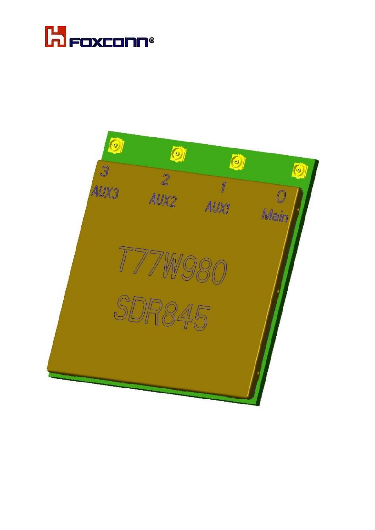
0
WWANMain
600~6000
1
WWAN MIMO 1
1700~2700
2
WWAN MIMO 2
1700~2700
3
WWAN Aux/GPS
600~6000
QTI single-chip RF device that supports uplink carrier aggregation (using two Tx chains)
QTI single-chip RF device that supports the integrated envelope tracking (ET) feature for both
Tx chains (ETDAC0 and ETDAC1)
QTI single-chip RF transceiver that supports up to five downlink (DL) carrier aggregation
One independent differential low noise amplifier (LNA) port, supporting Tx feedback for all
WAN bands (UL)
Most highly integrated RF transceiver
Up to 10 receivers running concurrently
Simplified DC power requirements for this highly integrated RFIC with built-in microprocessor
2.2 Antenna Design
The antenna elements are typically integrated into the notebook/ultrabook /tablet and connected to
T77W980T00module via flexible RF coaxial cables. T77W980T00 provides four RF connectors
(MHF4 type), one for the primary transmitter/receiver port and one for the diversity receiver and
GNSS the others for the 4*4 MIMO. To ensure customer has a clear knowledge of the four antennas,
check below product picture.
Figure 2-2-1 Antenna connector location and type
Page 17

COMPANY CONFIDENTIAL
17
Parameter
Min
Type
Max
Units
Storage temperature
-30
+25
+85
°C
Recommend operating temperature
(3GPP compliant with mitigation plan) (*1)
-30
+25
+70
°C
Extendable (with limited performance)
Temperature measure on T77W980 module(*2)
-40 +85
°C
3.1 commended operating conditions
Table 4-1 Recommended operating conditions
3.2 Storage Requirement
The module must be stored and sealed properly in vacuum package under a temperature below 40°
C and the relative humidity less than 90% in order to ensure the weldability within 12 months.
3.3 Crystal material
For T77W980T00 OEM main board crystal , please OEM choose the same material TXC
-OW38477001, when mount the GRC on the mother board, for OEM just redo the XO_Calibration,
and leverage the RF QCN parameter.
OEM vendor needs to set up a RF calibration station for crystal, Using IQXStream or 8820C to
re-calirbate the XO then rewrite the XO NV.
NV items list will provide later.
Figure 4-2 RF calibration station
Page 18

COMPANY CONFIDENTIAL
18
Specification / Requirements
Contact discharge
Air discharge
JEDEC JESD22-A114D
All SMT interfaces
± 1kV Human Body Model
n.a.
ETSI EN 301 489-1/7
All antenna interfaces
(LTE/WCDMA/GPS)
± 4kV
± 8kV
BATT+
± 4kV
± 8kV
4. Electrostatic Discharge
The module is not protected against Electrostatic Discharge (ESD) in general. Consequently, it is
subject to ESD handling precautions that typically apply to ESD sensitive components.
Proper ESD handling and packaging procedures must be applied throughout the processing,
handling and operation of any application that incorporates a T77W980T00 LTE module.
The remaining interfaces of T77W980T00 LTE module are not accessible to the user of the final
product (since they are installed within the device) and are therefore only protected according to the
JEDEC JESD22-A114D requirements.
T77W980T00 LTE module has been tested according to the following standards. Electrostatic values
can be gathered from the following table.
Table 4-5: Electrostatic values
Note: Please note that the values may vary with the individual application design. For example, it
matters whether or not the application platform is grounded over external devices like a computer or
other equipment
Page 19

COMPANY CONFIDENTIAL
19
5. Mechanics, Mounting and Packaging
5.1Mechanics
5.1.1 Overview
The T77W980T00 LTE module uses the 183-pin LGA as their external interface. For details about
the module and dimensions, see 5.1.2 Dimensions and Interfaces (Tolerance:+/-0.10).
Typical module dimension (W x L): 31mmx31mm. Max Z-height is 2.15mm
Pin1
Figure 5-1-1Top & side view
5.1.2 Dimensions and Interfaces
Figure 5-1-2 shows the dimensions in details.
Figure 5-1-2 Dimensions Top view (Unit: mm)
Page 20

COMPANY CONFIDENTIAL
20
5.1.2 Recommended LGA Land Pattern(bottom view), unit:mm
Page 21

COMPANY CONFIDENTIAL
21
5.1.3PCB stacking
10 Layers, HDI, thickness:0.8mm +/-0.05mm
5.1.4 label information
Page 22

COMPANY CONFIDENTIAL
22
5.2Mounting onto the Application Platform
This section describes how to mount T77W980T00 LTE Module onto the PCBs (=printed circuit
boards), includingland pattern and stencil design, board-level characterization, soldering conditions,
durabilityand mechanical handling.
Note: All SMT module pads need to be soldered to the application’s PCB. Not only must all supply
pads and signals be connected appropriately, but all pads denoted as “Do not use” will alsohave to be
soldered (but not electrically connected) in order to ensure the best possible mechanical stability.
5.2.1SMT PCB Assembly
5.2.1.1Land Pattern and Stencil
Recommended design of the solder pads on customers' PCBs (Unit: mm)
Non Solder Mask Defined (NSMD) is recommended. In addition, the solder mask of the NSMD pad
design is larger than the pad so the reliability of the solder joint can be improved.
Page 23

COMPANY CONFIDENTIAL
23
Figure 5-2-1Land pattern (top view)
It is recommended that the stencil for the LGA module be at least 0.15 mm in thickness. For
the recommended stencil aperture design, refer figure 5-2-1.(Unit: mm)
The solder paste dosage(0.1587g/pcs) is a theoretical value for reference.
5.2.1.2Board Level Characterization
Board level characterization issues should also be taken into account if devising an SMT process.
Characterization tests should attempt to optimize the SMT process with regard to board
levelreliability. This can be done by performing the following physical tests on sample boards:
Peeltest, bend test, tensile pull test, drop shock test and temperature cycling.
It is recommended to characterize land patterns before an actual PCB production, taking individual
processes, materials, equipment, stencil design, and reflow profile into account. For landand stencil
pattern design recommendations see also Section 5.2.1.1. Optimizing the solderstencil pattern design
and print process is necessary to ensure print uniformity, to decrease solder voids, and to increase
board level reliability.
Generally, solder paste manufacturer recommendations for screen printing process parameters and
reflow profile conditions should be followed. Maximum ratings are described in Section5.2.3.
5.2.2Moisture Sensitivity Level
T77W980T00 LTE Module comprises components that are susceptible to damage induced by
absorbed moisture.
Page 24

COMPANY CONFIDENTIAL
24
Profile Feature
Pb-Free Assembly
Preheat & Soak
Temperature Minimum (TSmin )
Temperature Maximum (TSmax )
Time (tSminto t Smax ) (tS )
150℃
180℃
60~120 seconds
Average ramp up rate (TSmax to TP )
3 K/second max
Liquidous temperature (TL )
Time at liquidous (tL )
217℃
50~90 seconds
Peak package body temperature (TP )
240~250℃
Time (tP ) within 5 °C of the peak package body
temperature (TP )
30 seconds max.
Average ramp-down rate (TP to TSmax )
3 K/second max.
Time 25°C to maximum temperature
8 minutes max.
T77W980T00 LTE Module complies with the latest revision of the IPC/JEDEC J-STD-020 Standard
for moisture sensitive surface mount devices and is classified as MSL 4.For additional MSL
(=moisture sensitivity level) related information see Section 5.2.4 and Section 5.3.2.
5.2.3Soldering Conditions and Temperature
5.2.3.1Reflow Profile
Figure 5-2-3: Reflow Profile
Table 5-2: Reflow temperature ratings
Page 25

COMPANY CONFIDENTIAL
25
5.2.3.2Maximum Temperature and Duration
The following limits are recommended for the SMT board-level soldering process to attach the
module:
• A maximum module temperature of 245°C. This specifies the temperature as measured atthe
module’s top side.
• A maximum duration of 30 seconds at this temperature.
Please note that while the solder paste manufacturers' recommendations for best temperature
and duration for solder reflow should generally be followed, the limits listed above must not be
exceeded.
T77W980T00 LTE Module is specified for one soldering cycle only.Once T77W980T00 LTE module
is removed from the application, themodule will very likely be destroyed and cannot be soldered onto
another application.
5.2.4Durability and Mechanical Handling
5.2.4.1Storage Life
T77W980T00 LTE modules, as delivered in tape and reel (TBD) carriers, must be stored in sealed,
moisture barrieranti-static bags. The shelf life in a sealed moisture bag is an estimated 12 month.
However, sucha life span requires a non-condensing atmospheric environment, ambient temperatures
below
40°C and a relative humidity below 90%. Additional storage conditions are listed in Table 3-1.
5.2.4.2Processing Life
T77W980T00 LTE module must be soldered to an application within 72 hours after opening the
MBB (=moisturebarrier bag) it was stored in.As specified in the IPC/JEDEC J-STD-033 Standard,
the manufacturing site processing themodules should have ambient temperatures below 30°C and a
relative humidity below 60%.
5.2.4.3 Baking
Baking conditions are specified on the moisture sensitivity label attached to each MBB (see
Figure 49 for details):
• It is not necessary to bake T77W980T00 LTE module , if the conditions specified in Section
5.2.4.1 and Section5.2.4.2 were not exceeded.
Page 26

COMPANY CONFIDENTIAL
26
• It is necessary to bake T77W980T00 LTE module , if any condition specified in Section 5.2.4.1
and Section 5.2.4.2 was exceeded.
If baking is necessary, the modules must be put into trays that can be baked to at least 125°C.
Devices should not be baked in tape and reel carriers at any temperature.
5.2.4.4 Electrostatic Discharge
ESD (=electrostatic discharge) may lead to irreversible damage for the module. It is
thereforeadvisable to develop measures and methods to counter ESD and to use these to control the
electrostatic environment at manufacturing sites.
Please refer to Section 4.5 for further information on electrostatic discharge.
5.3Packaging
5.3.1Tape and Reel(TBD)
The single-feed tape carrier for T77W980T00 LTE is illustrated in Figure 45. The figure also shows
the proper part orientation.
5.3.1.1 Orientation
Figure 5-3-1: Carrier tape
Figure 5-3-2: Roll direction
5.3.1.2Barcode Label
A barcode label provides detailed information on the tape and its contents. It is attached to thereel.
Figure 5-3-3: Barcode label on tape reel
5.3.2Shipping Materials
T77W980T00 LTE module is distributed in tape and reel carriers. The tape and reel carriers used to
distribute T77W980T00 LTE module are packed as described below, including the following required
shipping materials:
Page 27

COMPANY CONFIDENTIAL
27
• Moisture barrier bag, including desiccant and humidity indicator card
• Transportation bag
5.3.2.1Moisture Barrier Bag
The tape reels are stored inside an MBB (=moisture barrier bag), together with a humidity indicator
card and desiccant pouches - see Figure 48. The bag is ESD protected and delimits moisture
transmission. It is vacuum-sealed and should be handled carefully to avoid puncturing ortearing. The
bag protects the T77W980T00 LTE modules from moisture exposure. It should not be openeduntil
the devices are ready to be soldered onto the application.
Figure 5-3-4: Moisture barrier bag (MBB) with imprint
The label shown in Figure 5-3-5 summarizes requirements regarding moisture sensitivity, including
shelf life and baking requirements. It is attached to the outside of the moisture barrier bag.
Figure 5-3-5: Moisture Sensitivity Label
MBBs contain one or more desiccant pouches to absorb moisture that may be in the bag.
Thehumidity indicator card described below should be used to determine whether the
enclosedcomponents have absorbed an excessive amount of moisture.
The desiccant pouches should not be baked or reused once removed from the MBB.
The humidity indicator card is a moisture indicator and is included in the MBB to show the
approximate relative humidity level within the bag. Sample humidity cards are shown in Figure
5-3-6.If the components have been exposed to moisture above the recommended limits, the units
willhave to be rebaked.
Figure 5-3-6: Humidity Indicator Card - HIC
A baking is required if the humidity indicator inside the bag indicates 10% RH or more.
5.3.2.2Transportation Box
Page 28

COMPANY CONFIDENTIAL
28
Tape and reel carriers are distributed in a box, marked with a barcode label for identificationpurposes.
A box contains 2 reels with 500 modules each.
3. Sample Application
TBD
Page 29

COMPANY CONFIDENTIAL
8
GNSS
Customizable tracking session
• Automatic tracking session on startup
• Concurrent standalone GPS, GLONASS, Beidou and Galileo
• gpsOneXTRA with GPS + GLONASS + Beidou + Galileo support
1.2 Carrier aggregation combination
1.2.1. Refer to Qualcomm documents 80-P8641-123 Rev. A, Published: 2017/7/31.
Remark: T77W980 hardware design can support follow CA combination, but the Final CA
combinations plan depends on carrier engagement and Qualcomm software design.
1.2.2. Qualcomm SDX20 support 5CA+256QAM (up to Cat18) and Rel13 (FDD+TDD CA)
which is mandatory for AU/JP/China carriers.
Update the Carrier CA combination list later
1.3 System Block Diagram
Figure 1-3-1 GRC Architecture
1. GRC is the RF only module, it doesn’t include the CPU & memory. So GRC doesn’t have the SW
image.
2. Each GRC will have its unique QCN data, it will use the GRC SN or IMEI to name it, and provide
these data to one ftp server. OEM can scan the SN or IMEI to get the QCN data then load it to the
platform memory.
Host integration instructions
Install module through golden finger.
The End Host information:
MT code : 81JL
Marketing name : Lenovo YOGA C630-13Q50
Page 30

Federal Communication Commission Interference Statement
This device complies with Part 15 of the FCC Rules. Operation is subject to the
following two conditions: (1) This device may not cause harmful interference,
and (2) this device must accept any interference received, including
interference that may cause undesired operation.
This equipment has been tested and found to comply with the limits for a Class
B digital device, pursuant to Part 15 of the FCC Rules. These limits are
designed to provide reasonable protection against harmful interference in a
residential installation. This equipment generates, uses and can radiate radio
frequency energy and, if not installed and used in accordance with the
instructions, may cause harmful interference to radio communications.
However, there is no guarantee that interference will not occur in a particular
installation. If this equipment does cause harmful interference to radio or
television reception, which can be determined by turning the equipment off and
on, the user is encouraged to try to correct the interference by one of the
following measures:
- Reorient or relocate the receiving antenna.
- Increase the separation between the equipment and receiver.
- Connect the equipment into an outlet on a circuit different from that
to which the receiver is connected.
- Consult the dealer or an experienced radio/TV technician for help.
FCC Caution: Any changes or modifications not expressly approved by the
party responsible for compliance could void the user's authority to operate this
equipment.
This transmitter must not be co-located or operating in conjunction with any other
antenna or transmitter.
This device is intended only for OEM integrators under the following
conditions:
The antenna must be installed such that 20 cm is maintained between the antenna
and users, and
The transmitter module may not be co-located with any other transmitter or antenna.
As long as 2 conditions above are met, further transmitter test will not be required.
Page 31

However, the OEM integrator is still responsible for testing their end-product for any
additional compliance requirements required with this module installed
IMPORTANT NOTE: In the event that these conditions can not be met
certain laptop configurations or co-location with another transmitter), then the FCC
authorization is no longer considered valid and the FCC ID can not
final product. In these circumstances, the OEM integrator will be responsible for
re-evaluating the end product (including the transmitter) and obtaining a separate
FCC authorization.
End Product Labeling
This transmitter module is authorized only for use in device where the antenna may
be installed such that 20 cm may be maintained between the antenna and users. The
final end product must be labeled in a visible area with the following: “Contains FCC
ID:MCLT77W980”. The grantee's FCC ID can be used only when all FCC compliance
requirements are met.
(for example
be used on the
Manual Information To the End User
The OEM integrator has to be aware not to provide information to the end user
regarding how to install or remove this RF module in the user’s manual of the
end product which integrates this module.
The end user manual shall include all required regulatory information/warning
as show in this manual.
Radiation Exposure Statement:
This equipment complies with FCC radiation exposure limits set forth for an
uncontrolled environment. This equipment should be installed and operated
with minimum distance 20cm between the radiator & your body.
Industry Canada statement:
This device complies with ISED’s licence-exempt RSSs. Operation is subject to the
following two conditions: (1) This device may not cause harmful interference, and (2)
this device must accept any interference received, including interference that may
cause undesired operation.
Le présent appareil est conforme aux CNR d’ ISED applicables aux appareils radio
exempts de licence. L’exploitation est autorisée aux deux conditions suivantes : (1) le
dispositif ne doit pas produire de brouillage préjudiciable, et (2) ce dispositif doit
accepter tout brouillage reçu, y compris un brouillage susceptible de provoquer un
Page 32

Antenna spec:
Antenna
No.
1
2
3
4
5
Antenna Gain(dBi)
Please refer to below
table
Please refer to below
table
Please refer to below
table
Please refer to below
table
Please refer to below
table
Frequency
range (MHz)
Antenna Type
Connecter
Type
699~803 PIFA i-pex(MHF)
791~960
1447.9~1606
1710~2170
2500~2690
5110~5925
(for LAA RX)
PIFA i-pex(MHF)
PIFA i-pex(MHF)
PIFA i-pex(MHF)
2305~2315 Dipole i-pex(MHF)
Antenna gain list
Antenna
No.
Band Freq. Range (MHz) Gain (dBi)
3 WCDMA II (B2) 1850~1910 4.92
3 WCDMA IV (B4) 1710~1755 5.99
2 WCDMA V (B5) 824~849 2.68
3 LTE Band (2) 1850~1910 4.92
3 LTE Band (4) 1710~1755 5.99
2 LTE Band (5) 824~849 2.68
3 LTE Band (7) 2500~2570 5.2
1 LTE Band (12) 698~716 4.17
1 LTE Band (13) 777~787 3.05
1 LTE Band (14) 788~798 2.87
1 LTE Band (17) 704~716 4.17
3 LTE Band (25) 1850~1915 4.92
2 LTE Band (26) 814~849 2.92
5 LTE Band (30) 2305~2315 3.02
3 LTE Band (38) 2570~2620 4.82
3 LTE Band (41) 2496~2690 5.38
3 LTE Band (66) 1710~1780 5.99
1 LTE Band (71) 663~698 3.83
Cable
Length
100mm
100mm
100mm
100mm
80mm
 Loading...