HON HAI PRECISION IND T77H747 User Manual

COMPANY CONFIDENTIAL
1
Project Name
NFC (NXP NPC300) Module
Document Rev.
5.0
FOXCONN Part No.
T77H747.10
Module Rev.
005
FRU Part No.
01AX745
Customer Part No.
SW10K97523
FOXCONN Label Rev
00S0
Prepared by
Reviewed by
Approved by
Bandy.Jiang
Wei.Liao
Chang-Fu Lin
Revision Note
NFC
(Near Field Communication)
NXP NPC300 Module

COMPANY CONFIDENTIAL
2
Revision
Date
Originator
Comment
1.0
2016/01/28
Smile. Ming
Initial release
2.0
2016/04/20
Bandy.Jiang
1> Add pin 1 marking for mechanical drawing.
2> Add SM bus support in addition to I2C bus. (in
page 4,5)
3> Add description of pin9 (TX_PWR_REQ) signal
with active high 1.8V level output. (in page 15)
4> Change the PN of antenna connector from
BM05B-ACHSS-A-GAN-ETF(LF)(SN) to BM05B-
ACHKS-A-GAN-ETF(HF)
5> Update material in shielding drawing.
6> Following the latest schematic, update the
material description into BOM
7> Add Tray ID label, Carton label, Pallet label into
label information
8> Update packing information
3.0
2016/04/26
Bandy.Jiang
1> Update Module picture in page 18
2> Update packing information in page 23~24
3> Update vendor PN of host interface connector in
page 15
4.0
2016/06/24
Bandy.Jiang
1> Remove R5 from BOM.
2> Change Foxconn project name from T77H747.00
to T77H747.10
3> Change FRU part No. from 00JT548 to
01AX745.
4> Based on above change list, update module
picture, BOM, label contents and packing
information.
5.0
2016/06/28
Bandy. Jiang
1> Change Host JST part number from ACHR-05V-
A-S to ACHR-05V-A-K(HF) in page 14
Revision History
T77H747.10 is made in China,
Manufactured by HongFuJin Precision Industry Co., LTD
Manufacture Site: ChongQing
http://www.foxconn.com

COMPANY CONFIDENTIAL
3
Content
1.
INTRODUCTION ........................................................................................................................................................... 4
1.1
SCOPE ....................................................................................................................................................................... 4
1.2
FUNCTION.................................................................................................................................................................. 4
1.3
HARDWARE BLOCK DIAGRAM ....................................................................................................................................... 5
2.
ELECTRICAL CHARACTERISTICS ................................ ................................................................ ........................... 6
2.1
OPERATING CONDITIONS .............................................................................................................................................. 6
2.1
HOST INTERFACE CHARACTERISTICS .......................................................................................................................... 7
2.2
POWER-UP SEQUENCE ................................................................................................................................................ 8
2.3
POWER-DOWN SEQUENCE ........................................................................................................................................... 9
2.4
FUNCTION TIMING CHARACTERISTICS ......................................................................................................................... 9
3.
NFC CONTACTLESS STANDARD CONFORMANCE .......................................................................................... 10
3.1
FREQUENCY INTEROPERABILITY ................................................................................................................................ 10
3.2
SUPPORTED SMART CARD TYPES .............................................................................................................................. 10
3.3
CONTACTLESS INTERFACE UNIT ................................................................................................................................ 11
4.
MECHANICAL ARCHITECTURE .............................................................................................................................. 12
4.1
MODULE MECHANICAL DRAWING .............................................................................................................................. 12
4.2
ANTENNA INTERFACE OF NFC MODULE .................................................................................................................... 13
4.3.
HOST INTERFACE OF NFC MODULE ......................................................................................................................... 15
4.4.
SHIELDING COVER OF NFC MODULE ....................................................................................................................... 18
4.5.
PICTURE OF NFC MODULE ....................................................................................................................................... 18
5.
PCB PATTERN OF NFC MODULE .......................................................................................................................... 19
5.1
PCB COMPONENT PLACEMENT ................................................................................................................................. 19
5.2
PCB STACK UP AND MATERIALS .............................................................................................................................. 19
6.
BOM (BILL OF MATERIALS) OF NFC MODULE ................................................................................................... 20
7.
MARKING INFORMATION ........................................................................................................................................ 21
8.
PACKING INFORMATION ......................................................................................................................................... 23

COMPANY CONFIDENTIAL
4
1.
Introduction
The T77H747.10 is an NFC module designed for integration in computer or portable
equipment and consumer devices compliant with NFC standards (NFC Forum, NCI, ISO/IEC
14443 and ISO/IEC 15693) etc. This module is based on NXP NPC300 solution, which is a
highly integrated transmission module for contactless communication at 13.56MHz.
1.1 Scope
The NFC module RF protocols supported:
•
NFCIP-1, NFCIP-2 protocol
•
NFC Forum device 1.3
•
ISO/IEC 14443A, ISO/IEC 14443B
•
ISO/IEC 15693/ICODE VCD mode
•
FeliCa PCD mode/PICC mode
•
MIFARE PCD encryption mechanism(MIFARE 1K/4K)
•
MIFARE PICC mode
•
NFC Forum tag (type 1/type 2/type 3/type 4/type V)
1.2 Function
•
NFC Features
-
Reader & Writer mode
-
Peer-to-Peer Communication mode
-
Card emulation mode
•
I2C-bus and SM-bus compatible for host Interface
•
Windows 8 Logo Device Requirement compliant
-
NFC Forum Wave1 Certification
-
LLCP
-
SNEP
•
Windows 10 Logo system Requirement compliant
-
Peer to Peer Communication over 2cm distance less than 10cm
•
Modular certification
-
FCC
-
CE
-
UL/CB
-
meet other regulatory requirements (as defined by 108 countries)
(Remark: Regulatory Certification is not started at this phase)
•
Support Intel Windows 7/8.x/10 platform
•
RoHS and Green Compliant
COMPANY CONFIDENTIAL
5
1.3 Hardware block diagram
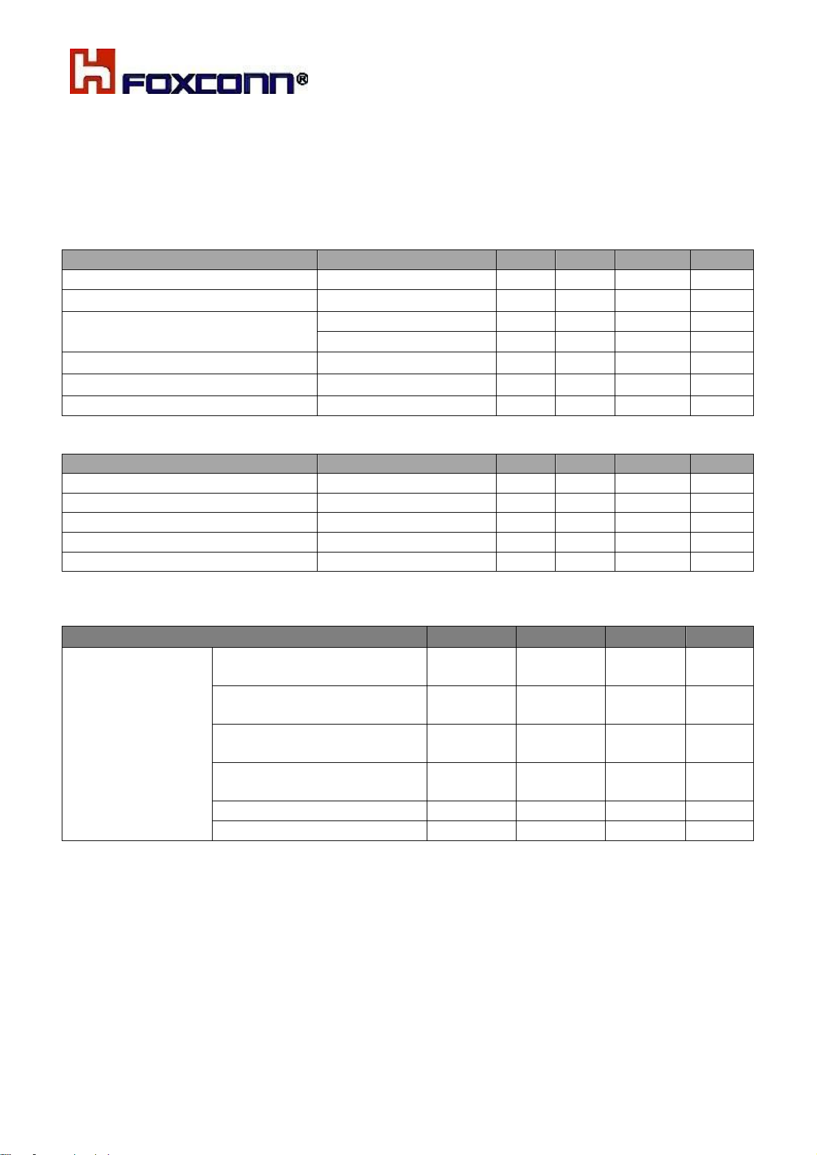
The T77H747.10 NFC module is based on NXP NPC300 solution with includes ARM
microcontroller core, EEPROM, demodulator and decoder, power management unit, host
interface. This module is powered from the host (5V) and interfaces to the host with I2C -bus
compatible signals, on-board 27.12 MHz XTAL. Also includes on board low profile FPC/FFC
12pin connector for host interface and 5pin WTB antenna connector for antenna interface.
Form factor: 20.0mm x13.0mm x 2.1mm (typical) NFC module
2
Host Interface: I C and SM bus compatible interface with 12-pin FPC connector
PCB: 4-layers HDI design
The functional block diagram is shown as below:
COMPANY CONFIDENTIAL
6
Symbol
Condition
Min.
Typ.
Max
Unit
VBAT
Respect to GND
--
5.0
6.0 V
PVDD
Respect to GND
--
3.3
4.35 V
ESD Limit Level
HBM
--
--
+/-1.0
KV
CDM
--
--
+/-500
V
Operating Temperature
-- 0
+25
+70
℃
Storage Temperature
--
-20
+25
+85
℃
Storage Humidity
-- 0
--
+85 %
Symbol
Condition
Min.
Typ.
Max
Unit
VBAT
Respect to GND
4.5
5.0
5.5 V
PVDD
Respect to GND
3.0
3.3
3.6 V
PMUVCC
Respect to GND
1.62
1.8
1.98 V
VDD
Respect to GND
1.65
1.8
1.95 V
VDD(SIM)
Respect to GND
1.62
1.8
1.98 V
Condition
Min.
Typ.
Max
Unit
Power
consumption
Reader mode
(PCD active)
--
130
--
mA
Reader mode
(PCD standby)
--
50
--
uA
Peer to peer mode
(active)
--
130
--
mA
Peer to peer mode
(standby)
--
50
--
uA
Continue TX mode
--
130
--
mA
Hard Power Down mode
--
10
--
uA
2.
Electrical Characteristics
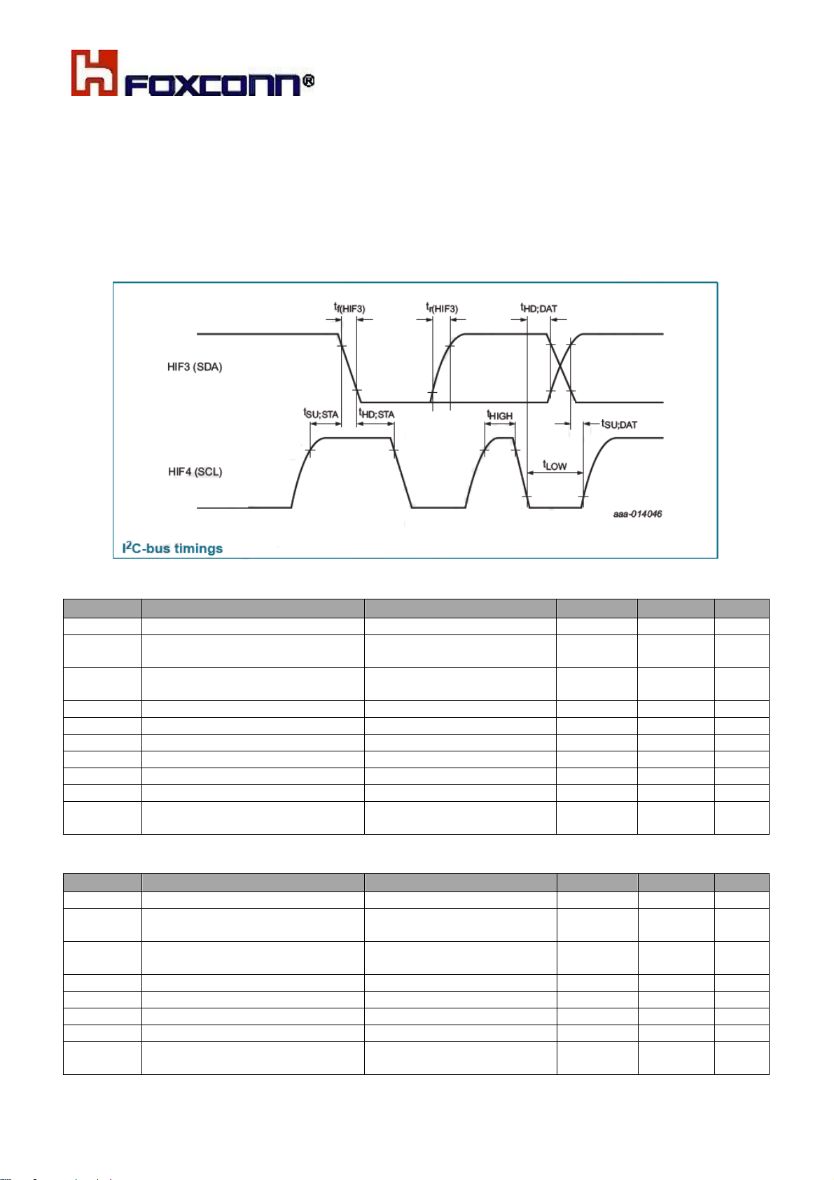
2.1 operating conditions
Absolute Maximum Rating
Recommended Operating Condition
Remark: VDD for TX_PWR_REQ referred voltage, VDD(SIM) for SWIO_UICC referred voltage.
Power Consumption
COMPANY CONFIDENTIAL
7
Symbol
Parameter
Conditions
Min
Max
Unit
f
CLK(HIF4)
Clock frequency on pin HIF4
I2C-bus SCL; C <100pF
b
0 3.4
MHz
t
SU;STA
Set-up time
for a
repeated
START condition
Cb<100pF
160 -
ns
t
HD;STA
Hold time(repeated) START
condition
Cb<100pF
160 -
ns
t
LOW
LOW period of the SCL clock
Cb<100pF
160 -
ns
t
HIGH
HIGH period of the SCL clock
Cb<100pF
60 -
ns
t
SU;DAT
Date set-up time
Cb<100pF
10 -
ns
t
HD;DAT
Data hold time
Cb<100pF
0 - ns
t
r(HIF3)
Rise time on pin HIF3
I2C-bus SDA; C <100pF
b
10
80
ns
t
f(HIF3)
Fall time on pin HIF3
I2C-bus SDA; C <100pF
b
10
80
ns
V
hys
Hysteresis voltage
Schmitt
trigger inputs;
Cb<100pF
0.1*VPVDD
- V
Symbol
Parameter
Conditions
Min
Max
Unit
f
CLK(HIF4)
Clock frequency on pin HIF4
I2C-bus SCL; C <400pF
b
0 400
KHz
t
SU;STA
Set-up time
for a
repeated
START condition
Cb<400pF
600 -
ns
t
HD;STA
Hold time(repeated) START
condition
Cb<400pF
600 -
ns
t
LOW
LOW period of the SCL clock
Cb<400pF
1.3 -
ns
t
HIGH
HIGH period of the SCL clock
Cb<400pF
600 -
ns
t
SU;DAT
Date set-up time
Cb<400pF
100 -
ns
t
HD;DAT
Data hold time
Cb<400pF
0 900
ns
V
hys
Hysteresis voltage
Schmitt
trigger inputs;
Cb<400pF
0.1* VPVDD
- V
2.1 Host interface characteristics
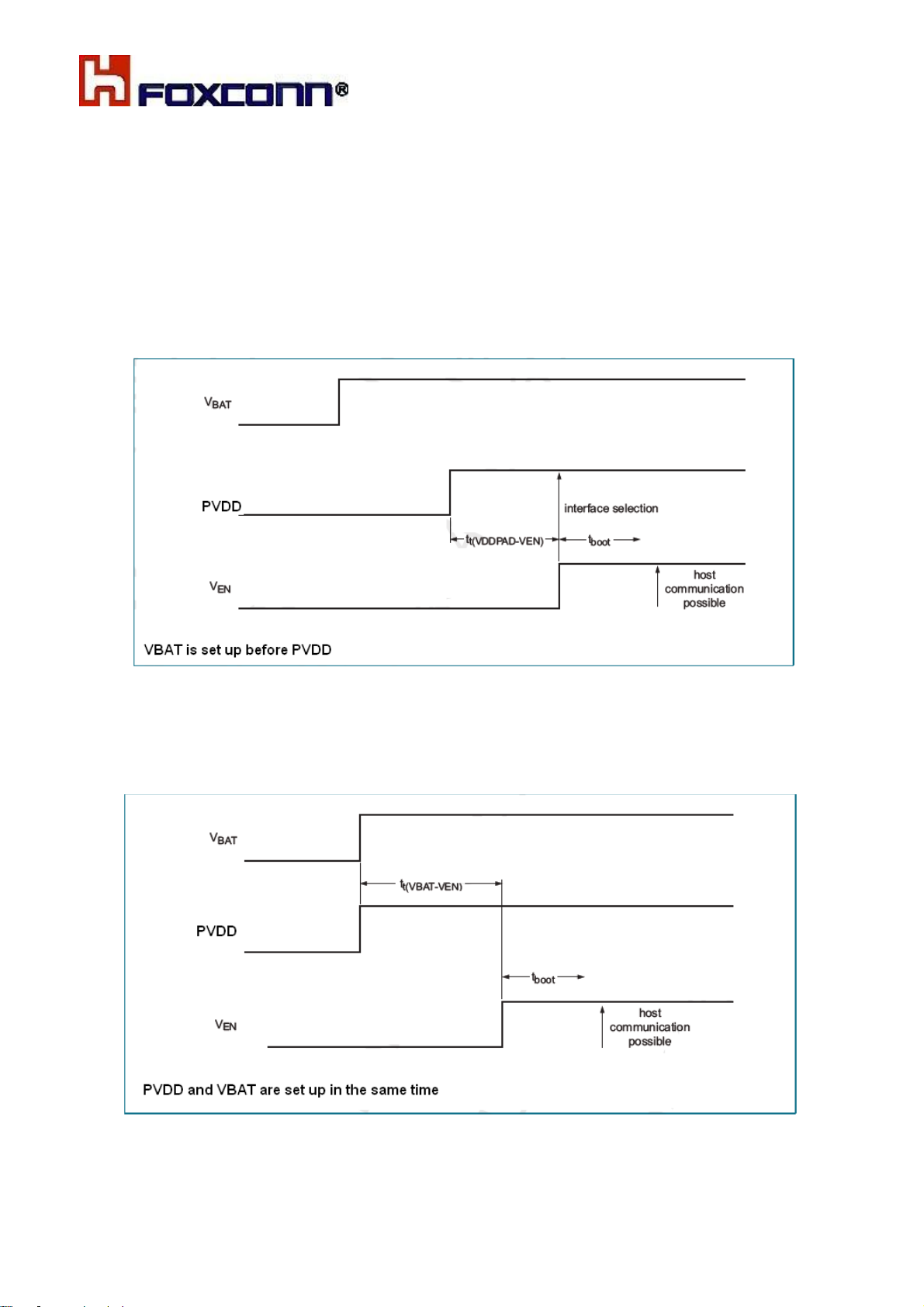
I2C-bus Interface
The I2C-bus Interface implements a slave I2C-bus interface with integrated shift register, shift timing generation
and slave address recognition.
I2C-bus Standard mode (100 KHz SCL), Fast mode (400 KHz SCL) and High-speed mode (3.4 MHz SCL) are
supported.
I2C-bus timings
Here below are timings and frequency specifications.
High-speed mode I2C-bus timing specification
Fast mode I2C-bus timing specification
COMPANY CONFIDENTIAL
8
2.2 Power-up sequence
There are 2 different supplies for module which allows set up independently, therefore
different power-up sequences have to be considered.
1> VBAT is set up before PVDD
This is at least the case when VBAT pin is directly connected to the battery and when
module VBAT is always supplied as soon the system is supplied.
As VEN pin is referred to VBAT pin, VEN voltage shall go high after VBAT has been set.
2> PVDD and VBAT are set up in the same time
It is at least the case when VBAT pin is connected to a PMU/regulator which also supplies
PVDD.
9
COMPANY CONFIDENTIAL
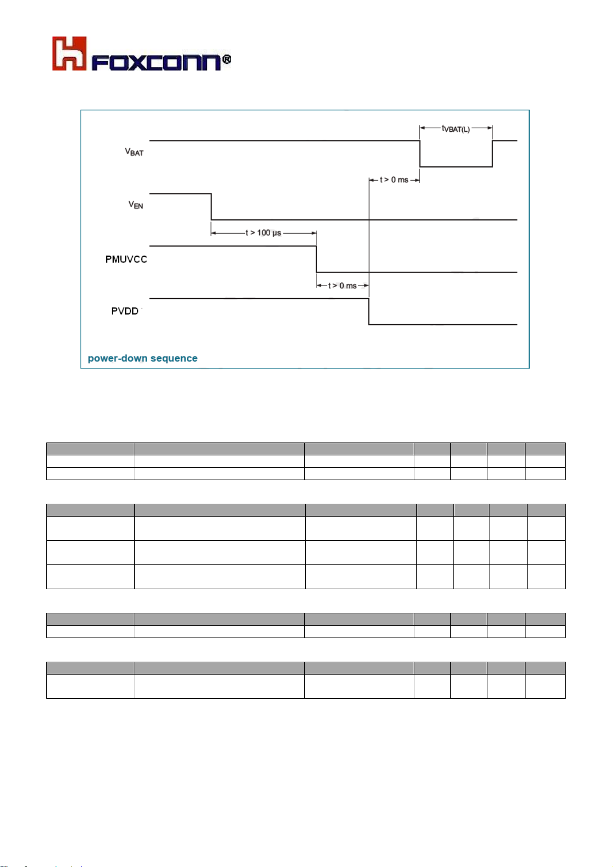
2.3 Power-down sequence
Symbol
Parameter
Conditions
Min
Typ
Max
Unit
t
W(VEN)
VEN pulse width
To reset
10 - -
us
t
boot
Boot time
- - 2.5
ms
Symbol
Parameter
Conditions
Min
Typ
Max
Unit
t
t(V
BAT
-VEN)
Transition time from pin VBAT to
pin VEN
VBAT,VEN
Voltage=HIGH
0 0.5 -
ms
t
t(V
PVDD
-VEN)
Transition time from pin PVDD to
pin VEN
PVDD,VEN
Voltage=HIGH
0 0.5 -
ms
t
t(V
BAT-VPVDD
)
Transition time from pin VBAT to
pin PVDD
VBAT,PVDD
Voltage=HIGH
0 0.5 -
ms
Symbol
Parameter
Conditions
Min
Typ
Max
Unit
t
VBAT(L)
Time V
BAT
LOW
20 - -
ms
Symbol
Parameter
Conditions
Min
Typ
Max
Unit
T
t(DWL_REQ-VEN)
Transition
time
from pin
DWL_REQ to pin VEN
DWL_REQ,VEN
voltage=HIGH
0 0.5 -
ms
2.4 Function timing characteristics
Reset timing
Power-up timings
Power-down timings
Download mode timings
 Loading...