HON HAI PRECISION IND T77H566 User Manual
COMPANY CONFIDENTIAL
Project Name
M.2 Type1216 BCM4356
WLAN + BT Combo Module
Foxconn Part No.
T77H566.01
Customer Model Name.
PK29S005P10
Product Revision
01S1
HON HAI PRECISION IND. CO., LTD.
No.2, 2nd Dong Huan Road, 10th
YouSong lndustrial District, Longhua
Town, Baoan, ShenZhen
Tel: +86-755-28128988#29413
Fax: +86-755-28129800#64886
Revision Note
WiFi/BT Module
WiFi/BT Module
Preliminary Datasheet
BCM4356 Dual-Band 2x2 802.11ac and Bluetooth v4.1
Combo Module
1

COMPANY CONFIDENTIAL
Preliminary Datasheet
Index
1. REVISION HISTORY ................................................................................................................................................... 3
2. INTRODUCTION .......................................................................................................................................................... 4
2.1 HARDWARE ARCHITECTURE .................................................................................................................................... 4
2.2 FEATURES ................................................................................................................................................................ 5
2.3 STANDARDS COMPLIANCE ....................................................................................................................................... 5
3. MECHANICAL SPECIFICATION .............................................................................................................................. 6
3.1 MECHANICAL DRAWING ............................................................................................................................................ 6
3.2 PCB STACK .............................................................................................................................................................. 6
3.3 RECOMMENDED LGA LAND PATTERN ..................................................................................................................... 7
3.4 RECOMMENDED STENCIL APERTURE ....................................................................................................................... 7
3.5 RF CONNECTOR TYPE ................................................................ ................................................................ ............. 8
3.6 RF CABLE ASSEMBLY NOTICE .................................................................................................................................. 9
3.7 RF PORT DEFINE ...................................................................................................................................................... 9
4. LGA PIN-OUT DEFINITION ..................................................................................................................................... 10
4.1 MODULE PIN-OUT DEFINITION ................................................................................................................................. 10
4.2 PIN DEFINITION ....................................................................................................................................................... 11
5. PRODUCT SPECIFICATION ................................................................................................................................... 13
5.1 DC ELECTRICAL SPECIFICATION ........................................................................................................................... 13
5.2 RF CHARACTERISTICS(TBD) ................................................................................................................................. 13
5.3 POWER UP SEQUENCE AND TIMING ...................................................................................................................... 15
5.3.1 Control signal Timing (WLAN=ON, BT=ON) ........................................................................................... 16
5.3.2 Control signal Timing (WLAN=OFF, BT=OFF) ....................................................................................... 16
5.3.3 Control signal Timing (WLAN=ON, BT=OFF) ......................................................................................... 17
5.3.3 Control signal Timing (WLAN=OFF, BT=ON) ......................................................................................... 17
5.3.4 WLAN Boot Up Sequence .......................................................................................................................... 17
5.4 UART HOST INTERFACE TIMING ........................................................................................................................... 18
5.5 PCM INTERFACE TIMING ....................................................................................................................................... 19
6.SCHEMATIC REFERENCE DESIGN ...................................................................................................................... 24
7. SOFTWARE REQUIREMENT(TBD) ....................................................................................................................... 26
8. REGULATORY(TBD) ................................................................................................................................................ 26
9. QUALITY ..................................................................................................................................................................... 26
10. PACKAGE INFORMATION ................................................................................................................................... 27
11. ENVIRONMENTAL REQUIREMENTS AND SPECIFICATIONS ..................................................................... 28
11.1 TEMPERATURE ..................................................................................................................................................... 28
11.2 PCB BENDING ...................................................................................................................................................... 28
11.3 HANDLING ENVIRONMENT .................................................................................................................................... 28
11.4 STORAGE CONDITION .......................................................................................................................................... 28
11.5 BAKING CONDITION .............................................................................................................................................. 28
11.6 SOLDERING AND REFLOW CONDITION .................................................................................................................. 29
2

Preliminary Datasheet
Date
Change Note
Author
REV Note
2014-07-25
Initial release(draft)
Robin Xu
0.1
2014-07-30
Add customer project code
Robin Xu
0.2
2014-08-21
1.Update the block diagram and support BTv4.1 in section2
2.Update the ME drawing in section3.1
3.Update the Recommended stencil aperture in setion3.4
Robin Xu
0.3
2014-11-14
Update WiFi Transmit Output Power
Ru-yan Li
0.4
2014-12-2
Add 3.7 RF port define
Ru-yan Li
0.5
2014-12-25
1.Update WLAN host interface description
2.Update BT RX sensitivity level
Ru-yan Li
0.6
1. Revision History
COMPANY CONFIDENTIAL
3
COMPANY CONFIDENTIAL
Form factor
M.2 Type 1216 LGA
Host Interface
WLAN: PCIe mode complies with PCI Express
base specification revision 3.0 for x1 lane and
power management running at Gen1 speeds.
BT: UART for data, PCM for audio
PCB
6-layer HDI design
RF connector
Two MHF-4 RF connectors on module
WiFi/BT Module
Preliminary Datasheet
2. Introduction
Project Name: M.2 Type 1216 BCM4356 WLAN+BT Combo Module
Project Number: T77H566.01
This documentation describes the engineering requirements specification of this M.2 1216 type module.
WLAN is compliant with IEEE 802.11 a/b/g/n and 2x2 IEEE 802.11ac MAC/ baseband/radio, Bluetooth is
compliant with Bluetooth v4.1+HS. This module takes advantage of the high throughput and extended range
of Broadcom MIMO solution It is a confidential document of Foxconn.
* For b/g/n and a/b/g/n module, Foxconn HW/FW is the same, platform use different firmware and driver
to enable or disable 5GHz 11ac function.
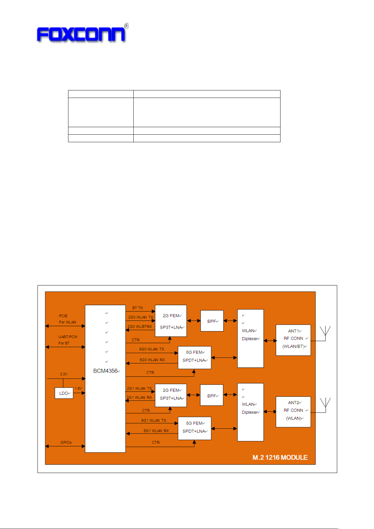
2.1 Hardware Architecture
The WLAN+BT combo module is designed base on BROADCOM BCM4356 chipset with external LNA for
both 2.4G and 5GHz. The BCM4356 is a complete dual-band (2.4GHz and 5GHz) Wi-Fi 2X2 MIMO
MAC/PHY/Radio System-on-a-Chip. This Wi-Fi single–chip device provides a high level of integration with
dual-stream IEEE 802.11ac MAC/baseband/radio, Bluetooth v4.1 + HS. In IEEE802.11ac mode, the WLAN
operation supports rates of MCS0-MCS9 (up to 256QAM) in 20MHz, 40MHz and 80MHz channels for data
rates up to 866.7Mbps. In addition, all the rates specified in IEEE802.11a/b/g/n are supported. See the
block diagram as below:
4

COMPANY CONFIDENTIAL
Preliminary Datasheet
2.2 Features
This module supports the following features:
IEEE 802.11a/b/g/n/ac dual-band 2x2 MIMO radio with virtual-simultaneous dual-band operation
Bluetooth v4.1+EDR with integrated class1 PA
Enhanced Bluetooth and WLAN coexistence performance
WLAN PCIe module complies with PCI express base specification for x1 lane and power management
running at Gen1 speeds.
Integrated ARMCR4
functionality minimizing the need to wake up the applications processor for standard WLAN functions.
This allows for further minimization of power consumption, while maintaining the ability to field upgrade
with features,
On-chip memory includes 768KB SRAM and 640KB ROM.
OneDriverTM software architecture for easy migration from existing embedded WLAN and Bluetooth
devices as well as future devices.
TX and RX low-density parity check (LDPC) support for improved range and power efficiency.
Supports IEEE802.11ac/n beam forming.
Bluetooth supports a high–speed UART interface(up to 4Mbps) and PCM for audio
Bluetooth Smart Audio technology improves voice and music quality to headsets
Bluetooth low power inquiry and page scan
Bluetooth low energy(BLE) support
Bluetooth Packet Loss Concealment(PLC)
Bluetooth Wide Band Speech(WBS)
GP/HF compliance
TM
processor with tightly coupled memory for complete WLAN subsystem
2.3 Standards Compliance
Bluetooth 2.1+EDR
Bluetooth 3.0+HS
Bluetooth 4.1(Bluetooth Low Energy)
IEEE802.11ac mandatory and optional requirements for 20MHz,40MHz and 80MHz channels
IEEE802.11n
IEEE802.11a
IEEE802.11b
IEEE802.11g
IEEE802.11d
IEEE802.11h
IEEE802.11i
Security
- WEP
- WPA/WPA2
- WMM/WMM-PS(U-APSD)/WMM-SA
- AES(Hardware Accelerator)
- TKIP(Hardware Accelerator)
- CKIP(SW support)
Proprietary Protocols
- CCXv2
- CCXv3
- CCXv4
- CCXv5
IEEE802.15.2 coexistence compliance-on silicon solution compliant with IEEE 3wire requirements
The module will the following future draft/standards:
IEEE802.11r-Fast Roaming (between APs)
IEEE802.11w-Secure Management Frames
IEEE802.11 Extensions:
- IEEE802.11e QoS Enhancements(In accordance with the WMM spec, QoS is already supported)
- IEEE802.11h 5GHz Extensions
- IEEE802.11i MAC Enhancements
- IEEE802.11k Radio Resource Measurement
5
COMPANY CONFIDENTIAL
Preliminary Datasheet
3. Mechanical Specification
3.1 Mechanical Drawing
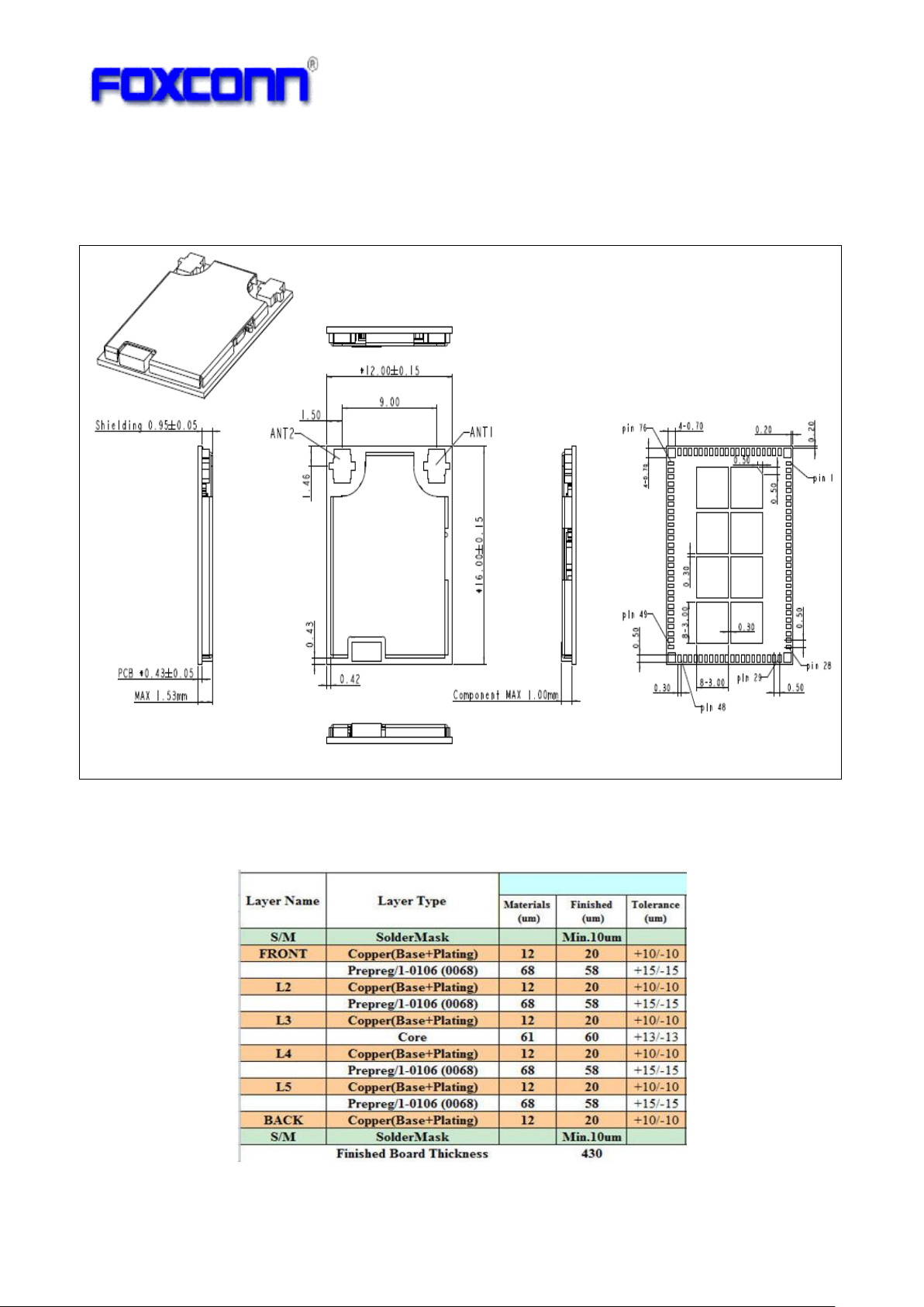
Typical module dimension (W x L): 12mmx16mm. Max Z-height is 1.53mm.
Unit:mm
3.2 PCB stack
6 Layers, HDI, thickness:0.43mm +/-0.05mm
6

COMPANY CONFIDENTIAL
Preliminary Datasheet
3.3 Recommended LGA Land Pattern
Unit: mm
TOP VIEW
Suggest use “solder-mask on pad” design for main-board to avoid the soldering short.
3.4 Recommended stencil aperture
Remark: Red stencil layer Green (pad layer)
Below is recommendation about respectively defined apertures as A,B,B`,C and C`
Stencil thickness=0.12mm
A=24*24 mil2 B=22*9 mil2 B`=24*9 mil2 C=40*40 mil2 C`=29.5*29.5mil2
Define space between apertures as D and E
D=11mil E=19.5mil
7
COMPANY CONFIDENTIAL
Antenna
Interface
Remark
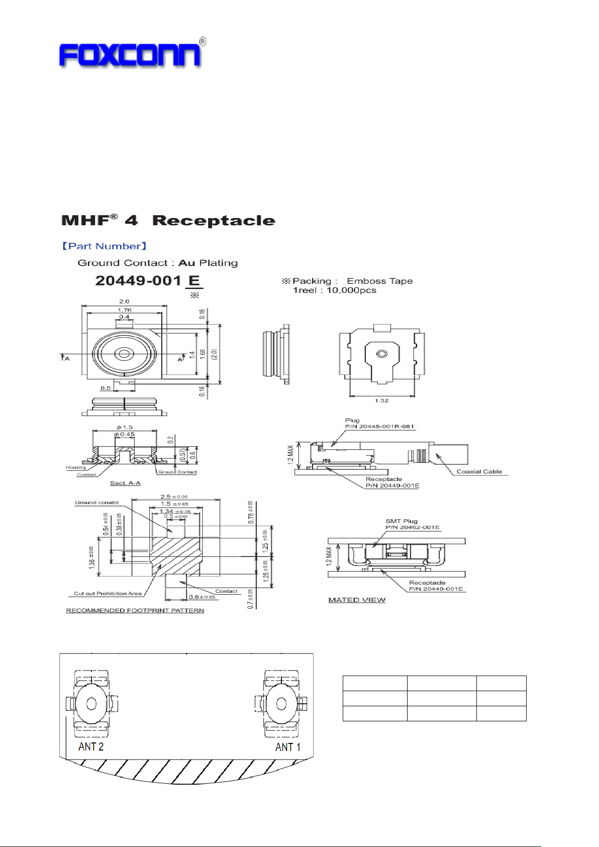
ANT1
WLAN/BT
Main
ANT2
WLAN
AUX
Preliminary Datasheet
3.5 RF Connector Type
The standard 2x2mm size RF receptacle connectors to be used in conjunction with the M.2
boards/modules
Same RF Receptacle on module supports either 0.81mm or 1.13mm diameter cable
Prefer to use 1.13mm diameter cable for lower cable loss
1.2mm max. mated height for low profile design
Example of IPEX RF connector
IPEX P/N: 20449-001E (MHF-4)
Antenna Placement
8
COMPANY CONFIDENTIAL
Preliminary Datasheet
3.6 RF cable assembly notice
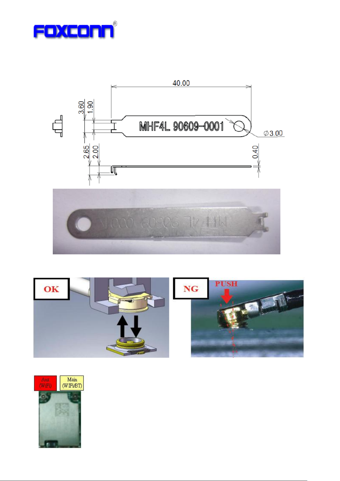
1> Mating/Unmating Jig
We recommend to use below Jig for mating/Unmating RF cable
2> Mating method of RF cable
Please push as gently as possible while mating plug with receptacle.
(The force must be 30N Max.)
3.7 RF port define
Main ANT for WiFi and BT, Aux ANT for WiFi.
9
COMPANY CONFIDENTIAL
96
95
94
93
92
91
90
89
88
87
86
85
84
83
82
81
80
79
78
77
105
GND
GND
GND
GND
GND
GND
GND
GND
GND
GND
GND
GND
GND
GND
GND
GND
GND
GND
GND
GND
GND
GND
108
1
NC
GND
76
2
NC
GND
75
3
NC
GND
74 4 3.3V
GND
GND
3.3V
73
5
3.3V 97
104 3.3V
72
6
GND
GND
71 7 NC
BT_USB_DP
70
8
NC
BT_USB_DN
69
9
NC
GND
68
10
NC
GND
GND
NC
67
11
NC 98
103 NC
66
12
NC
WLAN_LED_L
65
13
NC
BT_LED_L
64
14
NC
BT_REG_ON
63
15
NC
GND
62
16
NC
GND
GND
BT_PCM_CLK
61
17
GND 99
102 BT_PCM_OUT
60
18
NC
BT_PCM_IN
59
19
NC
BT_PCM_SYNC
58
20
GND
BT_UART_RTS_L
57
21
NC
BT_UART_RXD
56
22
NC
GND
GND
BT_UART_TXD
55
23
GND 100
101 BT_UART_CTS_L
54
24
BT_DEV_WAKE
BT_UART_HOST_
WAKE_L
53
25
NC
SDIO_CLK
52
26
GND
SDIO_CMD
51
27
SUSCLK(32KHz)
SDIO_DATA0
50
28
WL_RFDISABLE_L
SDIO_DATA1
49
106
GND
PCIE_PME_L
PCIE_CLKREQ_L
PCIE_PERST_L
GND
PCIE_REFCLKN
PCIE_REFCLKP
GND
PCIE_TDN
PCIE_TDP
GND
PCIE_RDN
PCIE_RDP
GND
VIO
NC
NC
WL_REG_ON
SDIO_WAKE_L
SDIO_DATA3
SDIO_DATA2
GND
107
29
30
31
32
33
34
35
36
37
38
39
40
41
42
43
44
45
46
47
48
Preliminary Datasheet
4. LGA Pin-out Definition
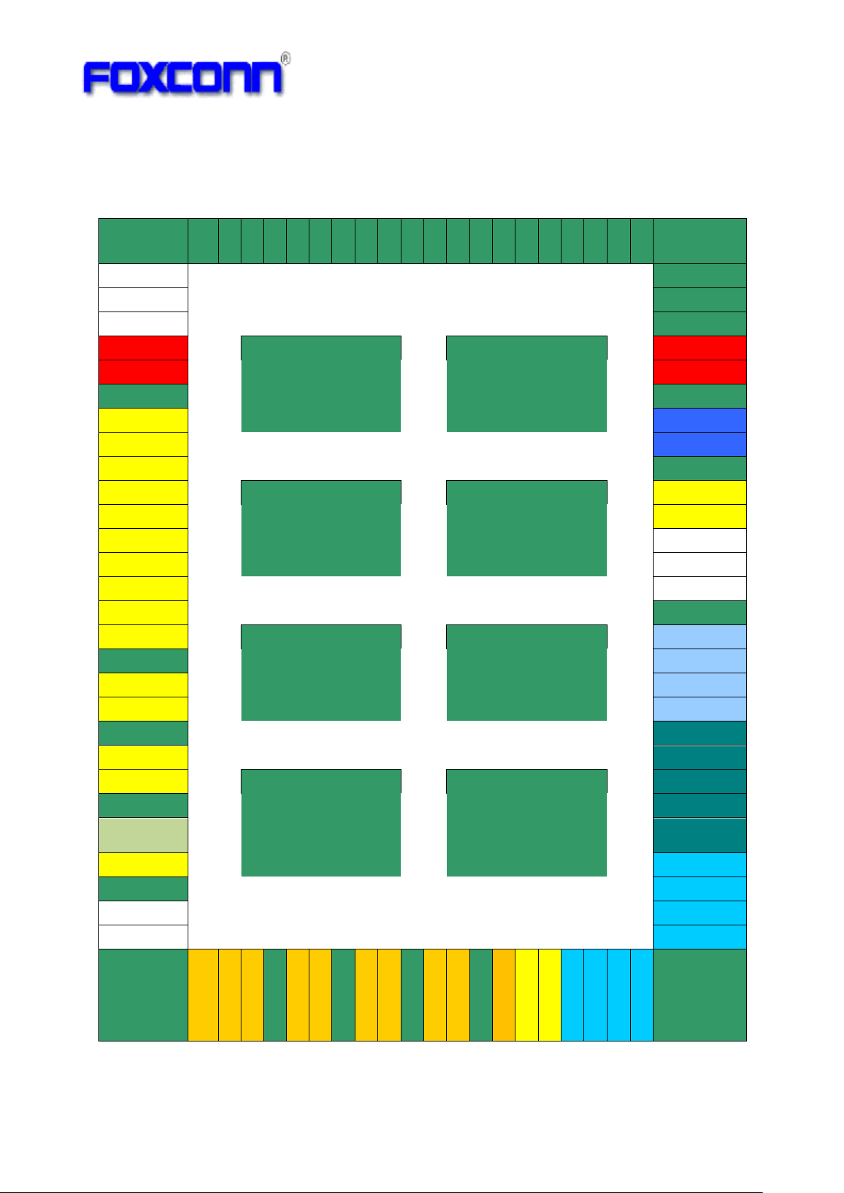
4.1 Module pin-out definition
Top view
10

Preliminary Datasheet
Pin No.
Pin Name
Type
Description
Voltage
Conne
cting
1-3, 7-16,
18,19,21,
22,25,
43-44,66,
67
NC - No connection
-
No
4,5,72,73
3.3V
Power
DC 3.3V power input
3.3V
Yes
24
BT_DEV_WAKE
I
Bluetooth device wake-up: Signal from the
host to the BCM4356 indicating that the host
requires attention.
• Asserted: The Bluetooth device must
wake-up or remain
awake.
• Deasserted: The Bluetooth device may
sleep when sleep criteria are met. The
polarity of this signal is software
configurable and can be asserted high or
low.
1.8V
Yes
27
SUSCLK (32KHz)
I
Suspend Clock is a 32.768 kHz clock supply
input that is provided by platform to enable
the add-in card to enter reduce power
consumption modes. SUSCLK will have a
duty cycle that can be as low as 30% or as
high as 70%. Accuracy will be up to
200ppm. See the detail spec in section6.
1.8V
(Note1)
Yes
28
WLAN_RFDISAB
LE_L
I
Active low, debounced signal when applied
by the system it will disable WLAN radio
operation on the add-in cards that implement
radio frequency applications. This signal is
internal pull-up on the card by default.
1.8V
(Note2)
No
29
PCIE_PME_L
OD
PCIe PME Wake. Open Drain with pull up on
platform; Active Low
1.8V
Yes
30
PCIE_CLKREQ_
L
OD
Clock Request is a reference clock request
signal as defined by the PCIe Mini Card CEM
specification; Also used by L1 PM Substates.
1.8V
Yes
31
PCIE_PERST_L
I
PE-Reset is a functional reset to the Add-In
card as defined by the PCIe Mini Card CEM
specification
1.8V
Yes
33
PCIE_REFCLKN
I
PCIe Reference Clock signals (100 MHz)
defined by the PCIe specification.
-
Yes
34
PCIE_REFCLKP
36
PCIE_TDN
O
PCIe TX differential signals defined by the
PCIe specification
-
Yes
37
PCIE_TDP
39
PCIE_RDN
I
PCIe RX differential signals defined by the
PCIe specification. Add AC cap 0.1uF on
PCIe signals of host side.
-
Yes
40
PCIE_RDP
42
VIO
Power
Reserved for external 1.8V power source
input. If don’t need, MUST keep it floating or
open
1.8V
(Note3)
Option
45
WL_REG_ON
I
SDIO sideband GPIO pin to enable/disable
(reset) the WiFi function. Platform firmware is
required to assert/de-assert this pin on every
boot (warm and cold). High active. See the
detail sequence timing in section5.3.
1.8V
Yes
46
SDIO_WAKE_L
O
SDIO Host Wake. Note in band SDIO wake is
not used for non-active modes, Active Low.
Require pull up on the host side
( recommended 15K to 100K )
1.8V
No
4.2 Pin definition
COMPANY CONFIDENTIAL
11
 Loading...