

Page 1

COMPANY CONFIDENTIAL REV 0.7
LTE PCI Express M.2 Module
95.1993T01
User Manual
version 0.7
- 1 -
Page 2

COMPANY CONFIDENTIAL REV 0.7
Table of Contents
1. INTRODUCTION ................................................................................................................................................... - 3 -
1.1 S
COPE
............................................................................................................................................................... - 3 -
1.2 F
UNCTION
2. SPECIFICATION ................................................................................................................................................... - 4 -
2.1 P
HYSICAL INTERFACE
2.2 P
IN ARRANGEMENT
3. PRODUCT REQUIREMENTS ............................................................................................................................ - 6 -
3.1 H
ARDWARE FEATURE
3.2 M
ECHANICAL SPECIFICATIONS
3.3 E
LECTRICAL SPECIFICATIONS
.......................................................................................................................................................... - 3 -
....................................................................................................................................... - 4 -
........................................................................................................................................... - 4 -
....................................................................................................................................... - 6 -
........................................................................................................................ - 11 -
.......................................................................................................................... - 11 -
- 2 -
Page 3

COMPANY CONFIDENTIAL REV 0.7
B41 (20+20) contiguous
B41 (20+20+20) contiguous
B
25 (5+5) non
-
contiguous
B25 (5+10) non
-
contiguous
1. Introduction
Project Name: LTE PCI Express M.2 Module
Foxconn Project Code: 95.1993T01
This documentation describes the hardware, and mechanical requirements specification of
LTE PCI Express M.2 Module. It is a confidential document of Foxconn.
1.1 Scope
The function of this module provides a LTE wireless WAN interface to access the internet,
and it is fully compliant with LTE specification (3GPP Release 12).
1.2 Function
LTE Standards 3GPP standard
Operating Frequency Band 25: 1930 to 1995 MHz (DL),
1850 to 1915 MHz (UL)
Band 41: (L) 2500 to 2570 MHz (DL/UL)
(H) 2620 to 2690MHz (DL/UL)
Number of T/Rx interface: Band 25: 2Tx /8Rx
Band 41L/H: 4Tx /8Rx
Channel Bandwidth: 5, 10, 15, 20 MHz for Band 41
5, 10, 15, 20 MHz for Band 25
Carrier Aggregation
DL carrier aggregation UL carrier aggregation
B41 (20+20) contiguous and non-contiguous
B41 (20+15) contiguous and non-contiguous
B41 (15+20) contiguous and non-contiguous
B41 (20+10) contiguous and non-contiguous
B41 (10+20) contiguous and non-contiguous
B41 (20+5) contiguous and non-contiguous
B41 (5+20) contiguous and non-contiguous
B41 (15+15) contiguous and non-contiguous
(hardware design can support above CA combination, but the final CA combinations plan
depends on carrier engagement and software design.)
B41 (10+15) contiguous and non-contiguous
B41 (15+10) contiguous and non-contiguous
- 3 -
Page 4
COMPANY CONFIDENTIAL REV 0.7
2. Specification
2.1 Physical Interface
RGMII, PCI express M.2 module,
PCB size: 64.4 mm x 65 mm
Antenna connector: UFL connector *8
Dual SIM interface (one for testing)
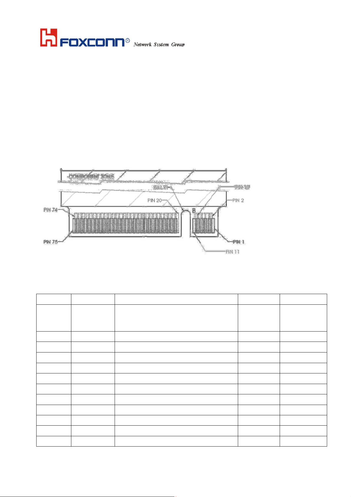
2.2 Pin Arrangement
Figure 2.1 the sequence of pins on the 75-pin signal interface of M.2 Key.B.
(Input: Carrier board to Module)
(Output: Module to Carrier board)
(Bi-direction: both direction among module and carrier board)
Pin number pin name description direction Voltage Domain
Select SIM0 or SIM1
1 SIM_SEL
2 3.6V_AUX power input VCC = 3.6V
3 GND ground NA NA
4 3.6V_AUX power input VCC = 3.6V
5 GND ground NA NA
6 PWR_EN enable/disable PMIC Input PU(VCC=3.6V)
7 USB2.0_DP USB2.0 D+ signal Bi-Direction
8 DCDC_1.8V power Output 1.8V
9 USB2.0_DM USB2.0 D- signal Bi-Direction
10 VBUS USB VBUS NA floating
· SIM_SEL Open or HIGH = SIM0 is active
· SIM_SEL LOW = SIM1 is active
Input OD, PU(1.8V)
11 GND ground NA NA
12 NA NA NA NA
- 4 -
Page 5

COMPANY CONFIDENTIAL REV 0.7
13 NA NA NA NA
14 NA NA NA NA
15 NA NA NA NA
16 NA NA NA NA
17 NA NA NA NA
18 NA NA NA NA
19 NA NA NA NA
20 SIM1_RST_O Test SIM reset Output SIM1 VCC
21 GND ground NA NA
22 SIM1_CLK_O Test SIM clock Output SIM1 VCC
23 UART0_RXD UART0 serial receive data Input 1.8V
24 SIM1_DAT_O Test SIM data Bi-Direction SIM1 VCC
25 UART0_TXD UART0 serial transmit data Output 1.8V
26 SIM_VCC1 Test SIM power output SIM1 VCC
27 GND ground NA
28 GPD2_21 GPIO for future use NA 1.8V
29 3.6V_AUX power input VCC = 3.6V
30 SIM0_RST LTE SIM reset Output SIM0 VCC
31 3.6V_AUX power input VCC = 3.6V
32 SIM0_CLK LTE SIM clock Output SIM0 VCC
33 GND ground NA NA
34 SIM0_DAT LTE SIM data Bi-Direction SIM0 VCC
35 3.6V_AUX power input VCC = 3.6V
36 SIM_VCC0 SIM power output SIM0 VCC
37 3.6V_AUX power input VCC = 3.6V
38 10MS_PULSE GPIO(1PPS PULSE) Output 1.8V
39 GND ground NA NA
40 RGMII_RCTL RGMII Interface Input 1.8V
41 3.6V_AUX power input VCC = 3.6V
42 RGMII_RCLK RGMII Interface Input 1.8V
43 3.6V_AUX power input VCC = 3.6V
NA
44 RGMII_MDIO RGMII Interface Input 1.8V
45 GND ground NA
46 RGMII_MDC RGMII Interface Output 1.8V
47 Default_Fact factory default Input 1.8V
48 RGMII_TCLK RGMII Interface Output 1.8V
49 GPD2_0 GPIO for future use NA 1.8V
50 RGMII_TCTL RGMII Interface Output 1.8V
NA
- 5 -
Page 6

COMPANY CONFIDENTIAL REV 0.7
51 GND ground NA
52 NA NA NA floating
53 GPD2_1 GPIO for future use NA 1.8V
54 RGMII_RXD3 RGMII Interface Input 1.8V
55 GPD2_2 GPIO for future use NA 1.8V
56 RGMII_RXD2 RGMII Interface Input 1.8V
NA
57 GND ground NA
58 RGMII_RXD1 RGMII Interface Input 1.8V
59 GPD2_3 GPIO for future use NA 1.8V
60 RGMII_RXD0 RGMII Interface Input 1.8V
61 GPD2_4 GPIO for future use NA 1.8V
62 RGMII_TXD3 RGMII Interface Output 1.8V
63 GPD2_5 GPIO for future use NA 1.8V
64 RGMII_TXD2 RGMII Interface Output 1.8V
65 GPD2_6 GPIO for future use NA 1.8V
66 RGMII_TXD1 RGMII Interface Output 1.8V
67 RESET#_KEY Reset signal (Active LOW) input PU(1.8V)
68 RGMII_TXD0 RGMII Interface Output 1.8V
69 GPD2_7 GPIO for future use NA 1.8V
70 3.6V_AUX power input VCC = 3.6V
71 GND ground NA NA
72 3.6V_AUX power input VCC = 3.6
73 GND ground NA NA
NA
74 3.6V_AUX power input VCC = 3.6V
75 GND ground NA NA
3. Product Requirements
3.1 Hardware Feature
3.1.1 Baseband processor: GDM7243A
GDM7243A is a highly integrated System-on-a-Chip (SOC) designed to support Long Term
Evolution (LTE). It includes a LTE baseband, high performance dual Cortex-a7 processor and
radio transceivers.
Dual processor architecture: Application CPU + Modem CPU (LTE)
RGMII/USIM/UART interface
Supports NAND Flash Interface
- 6 -
Page 7

COMPANY CONFIDENTIAL REV 0.7
LTE Features:(Internal: 4Rx-2TX; External: 4Rx-2TX)
8RX Diversity
TDD/FDD
3.1.2 RF transceiver: GRF7243A
GRF7243A is a fully integrated RF transceiver, all required PLL/VCO/loop filters are
integrated. Patented direct-conversion RF architecture with CMOS integration and minimizing
external BOM cost.
Supports all LTE bandwidth with multiple bandwidth channel selection filter
5/10/15/20MHz
RX saw-less architecture except UHB
TX single-ended port except UHB
3.1.3 PMIC: G5851
The G5851 provide a complete power supply solution, it contains 4 dc/dc converters and 7
LDOs. All channels DC/DC converters operate at one fixed frequency of 3.0MHz. The G5851
features an I2C compatible interface.
2.8V ~ 5.5V Input Voltage Operation.
Built-In Power ON/OFF Sequence for PMU.
7-channel LDOs are Programmable to Voltage Options by I2C.
SIM Card I/F Level Shifter
3.1.4 MCP
NAND Flash Density: 2-Gbits
Operating voltage : 1.7V to 1.95V
Operating Temperature : -25℃~ +85℃
Organization :
- Memory cell array: 2176 x 128K x 8
- Register: 2176 x 8
- Page size: 2176 bytes
- Block size: (128K + 8K) bytes
- 8bit ECC
Mobile DDR2 SD RAM Density: 2-Gbit
Operating voltage: 1.7V to 1.95V
Operating Temperature: -25 ~ +85℃ ℃
Speed: 533Mbps
- 7 -
Page 8

COMPANY CONFIDENTIAL REV 0.7
3.1.6 USIM
Off-board USIM connector supported. This module provides the dual SIM interface, and it
can be selected by SIM_SEL pin (the pin 1 of M.2 connector).
SIM_SEL(internally pull up)
State SIM selection
High SIM0
Low SIM1
3.1.7 RF CONNECTOR
Figure 3.1 RF connector location and description
- 8 -
Page 9

Figure 3.2 RF connector detailed information
COMPANY CONFIDENTIAL REV 0.7
- 9 -
Page 10

COMPANY CONFIDENTIAL REV 0.7
ANT Support Band TX RX Remark
# 0 25,41L, 41H 25,41L,41H 25,41L,41H TDD/FDD
# 1 25,41L, 41H NA 25,41L,41H TDD/FDD
# 2 25,41L, 41H 41L,41H 25,41L,41H TDD/FDD
# 3 25,41L, 41H NA 25,41L,41H TDD/FDD
# 4 25,41L, 41H 41L,41H 25,41L,41H TDD/FDD
# 5 25,41L, 41H 25 25,41L,41H TDD/FDD
# 6 25,41L, 41H 41L,41H 25,41L,41H TDD/FDD
# 7 25,41L, 41H NA 25,41L,41H TDD/FDD
And this module supports TX antenna switching as below,
(Each “+” indicates a separate TX path)
- 10 -
Page 11

COMPANY CONFIDENTIAL REV 0.7
3.2 Mechanical Specifications
3.2.1 Overview
The golden finger of 95.1993T01 is compatible with the NGFF 75 pin card edge-type
connector. Refer to NGFF Electromechanical Specification Revision P12 with Input Power
and Voltage Tolerance ECN for more details.
3.2.2 Mechanical constraints
Figure 3.3 Shows the mechanical constraints of 95.1993T01
3.3 Electrical Specifications
Parameter Min Type Max Units
Storage Temperature -30 +25 +85 ℃
Recommend operating temperature
(3GPP compliant)
Extendable (with limited performance) -40 +85 ℃
Operating Voltage 3.42 3.6 3.78 V
*Temperature measured on 95.1993T01 module
Table 3.1 Recommended operating conditions
Remark:
1. Extendable operation allows normal mode data transmission for limited time within the
extendable temperature range (outside the operating temperature range) the specified
electrical characteristics may be degraded.
2. Due to temperature measurement uncertainly, a tolerance on the stated shutdown thresholds
may occur. The possible deviation is in the range of +/- 2
-10 +25 +55 ℃
℃ at the over-temperature and
under-temperature limit.
- 11 -
Page 12

COMPANY CONFIDENTIAL REV 0.7
3. Need implement thermal solution on Platform (Example: add thermal pad to heat dissipated
from LTE module to Platform PCB) would get more thermal margin and benefit then extend the
operating temperature
4. Operating 95.1993T01 device under conditions beyond its absolute maximum ratings (Table
3-1) may damage the device. Absolute maximum ratings are limiting values to be considered
individually when all other parameters are within their specified operating ranges.
Functional operation and specification compliance under any absolute maximum condition, or
after exposure to any of these conditions, is not guaranteed or implied. Exposure may affect
device reliability
3.3.1 RF performance specifications
RF performance for 95.1993T01:
DL MCS: up to 256-QAM
UL MCS: up to 64-QAM
Uplink MIMO 2x2
Downlink MIMO 4x4
Compliance with 3GPP Rel. 12, in particular TS36.101
Transmission modes: TM1, 2, 3, 4, 5, 6, 7, 8, 9
TM3: 2/3/4 layers MIMO
TM4: 2/3/4 layers MIMO
TM9: 2/3/4 layers MIMO, up to eight CSI-RS
- 12 -
Page 13

COMPANY CONFIDENTIAL REV 0.7
OEM/Integrators Installation Manual
Important Notice to OEM integrators
1. This module is limited to OEM installation ONLY.
2. This module is limited to installation in mobile or fixed applications, according to Part 2.1091(b).
3. The separate approval is required for all other operating configurations, including portable
configurations with respect to Part 2.1093 and different antenna configurations
4. For FCC Part 15.31 (h) and (k): The host manufacturer is responsible for additional testing to verify
compliance as a composite system. When testing the host device for compliance with Part
15 Subpart B, the host manufacturer is required to show compliance with Part 15 Subpart B while the
transmitter module(s) are installed and operating. The modules should be transmitting and the evaluation
should confirm that the module's intentional emissions are compliant (i.e. fundamental and out of band
emissions). The host manufacturer must verify that there are no additional unintentional emissions other
than what is permitted in Part 15 Subpart B or emissions are complaint with the transmitter(s) rule(s).
End Product Labeling
When the module is installed in the host device, the FCC ID label must be visible through a window on
the final device or it must be visible when an access panel, door or cover is easily re-moved. If not, a
second label must be placed on the outside of the final device that contains the following text: “Contains
FCC ID: MCL951993A”
The FCC ID can be used only when all FCC compliance requirements are met.
Antenna Installation
(1) The antenna must be installed such that 20 cm is maintained between the antenna and users,
(2) The transmitter module may not be co-located with any other transmitter or antenna.
(3) To comply with FCC regulations limiting both maximum RF output power and human exposure to
RF radiation, the maximum antenna gain including cable loss in a mobile exposure condition must not
exceed:
Standalone Condition:
。 6.5 dBi in LTE B25
。 11.5 dBi in LTE B41
Assuming collocated with an ordinary WLAN transmitter with 5 dBi antenna gain
。 6.5 dBi in LTE B25
。 10.0 dBi in LTE B41
In the event that these conditions cannot be met (for example certain laptop configurations or co-location
- 13 -
Page 14

COMPANY CONFIDENTIAL REV 0.7
with another transmitter), then the FCC authorization is no longer considered valid and the FCC ID
cannot be used on the final product. In these circumstances, the OEM integrator will be responsible for
re-evaluating the end product (including the transmitter) and obtaining a separate FCC authorization.
Manual Information to the End User
The OEM integrator has to be aware not to provide information to the end user regarding how to install
or remove this RF module in the user’s manual of the end product which integrates this module. The end
user manual shall include all required regulatory information/warning as show in this manual.
Federal Communication Commission Interference Statement
This device complies with Part 15 of the FCC Rules. Operation is subject to the following two conditions:
(1) This device may not cause harmful interference, and (2) this device must accept any interference
received, including interference that may cause undesired operation.
This equipment has been tested and found to comply with the limits for a Class B digital device, pursuant
to Part 15 of the FCC Rules. These limits are designed to provide reasonable protection against harmful
interference in a residential installation. This equipment generates, uses and can radiate radio frequency
energy and, if not installed and used in accordance with the instructions, may cause harmful interference
to radio communications. However, there is no guarantee that interference will not occur in a particular
installation. If this equipment does cause harmful interference to radio or television reception, which
can be determined by turning the equipment off and on, the user is encouraged to try to correct the
interference by one of the following measures:
- Reorient or relocate the receiving antenna.
- Increase the separation between the equipment and receiver.
- Connect the equipment into an outlet on a circuit different from that to which the receiver is connected.
- Consult the dealer or an experienced radio/TV technician for help.
Any changes or modifications not expressly approved by the party responsible for compliance could void
the user's authority to operate this equipment. This transmitter must not be co-located or operating in
conjunction with any other antenna or transmitter.
Radiation Exposure Statement
This equipment complies with FCC radiation exposure limits set forth for an uncontrolled environment.
This equipment should be installed and operated with minimum distance 20 cm between the radiator &
your body.
- 14 -
 Loading...