

Page 1
wealth of peripherals that include NFC, USB and multiple interface options including Quad SPI (QSPI).
it also has high-end security features included to achieve best in clas security with an ARM
CryptoCEll cryptographic
system on chip and a full AES 128-bit encryption suite ., it also support BLE mesh
Full Bluetooth 5 support for long range Processing power and flash flexibility
Multiprotocol radio Power Efficiency
Bluetooth 5 ready multi-protocol radio
IEEE 802.15.4 radio support
32-bit ARM Cortex-M4F @ 64MHz
Up to 111 dB link budget for Bluetooth long range mode
Full-speed 12Mbs USB controller
NFC Tag-A
Software stacks available as downloads
Programmable output power from +8dBm to -20dBm
On-air compatible with nRF51, nRF24L and nRF24AP
High-precision RSSI
128 bit AES/ECB/CCM/AAR co-processor
Single-ended antenna output (on-chip balun)
Software stacks available as downloads
Application development independent of protocol stack
Wide supply voltage range + 1.7V to 5.5V
QSPI/SPI/2-wire/I²S/PDM/QDEC
Programmable Peripheral Interface - PPI
High speed SPI interface 32MHz
Quad SPI interface 32MHz
EasyDMA for all digital interfaces
RAM mapped FIFO using EasyDMA
12bit/200K SPS ADC
On-chip DC-DC buck converter
Quadrature demodulator
-96dBm Sensitivity for Bluetooth low energy
Arm CryptoCell CC310 crytographic security module
QSPI/SPI/2-wire/I²S/PDM/QDEC
Internet of Things (IoT)
SmartHome sensors
Computer peripherals
A4WP ‘Rezence’ wireless charging
Sports and fitness sensors and hubs
Smart watches
Interactive games
Wearables
Connected white goods
Voice-command smart remotes
Beacons
Connected health products
RC Toys
Building automation and sensor networks
User manual--NRF52840
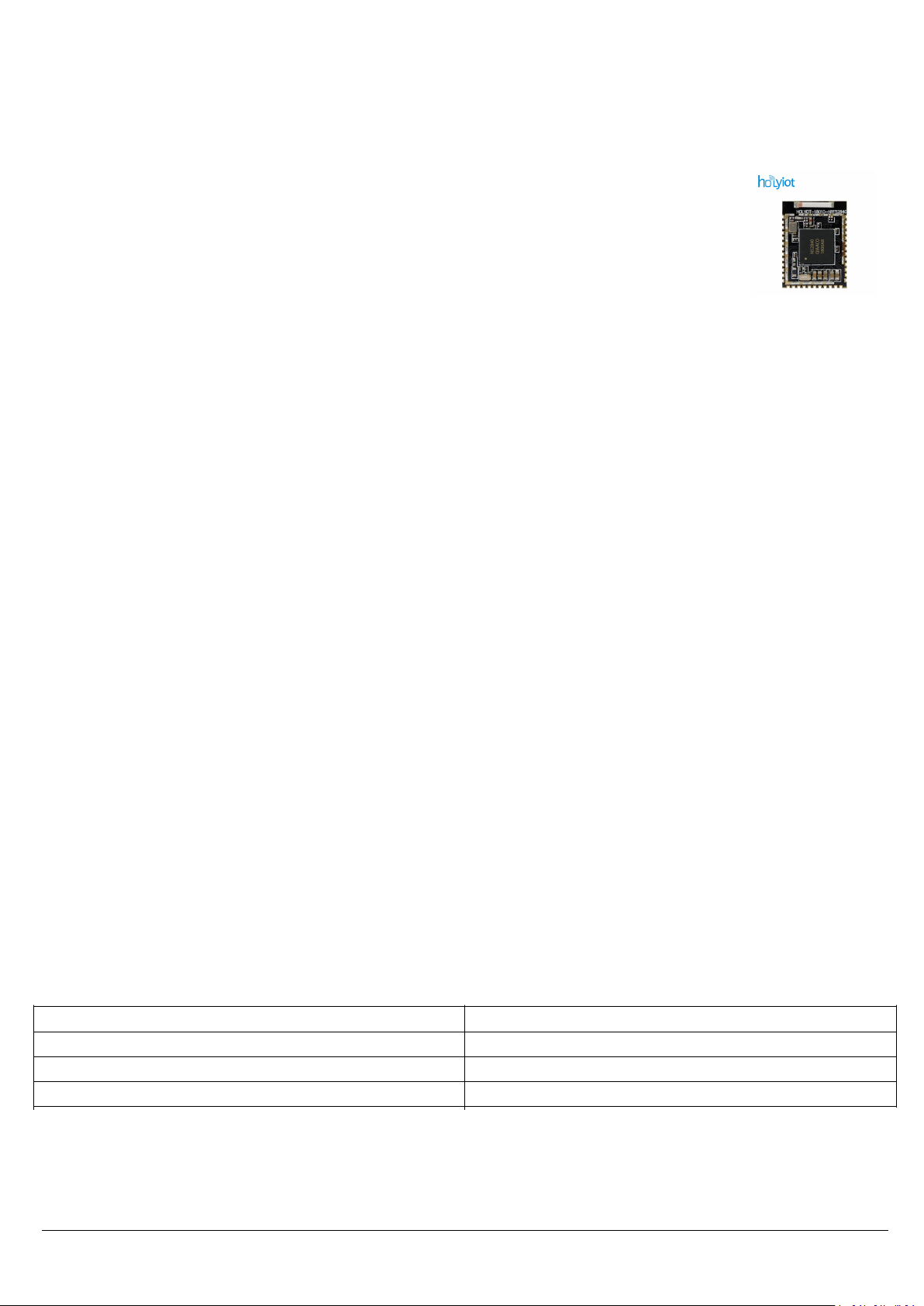
NRF52840
SoC , with ARM Cortex-M4 CPU , which has floating Point unit (FPU), 1MB flash with cache and 256kB RAM, It offers a
is powerful, highly flexible ultra-low power BLuetooth low energy(BLE module) using Nordic NRF52840
Specifications:
- 2Mbps
- Long range
- Advertising extensions
- Improved coexistence (CSA #2)
- Thread
- Zigbee
Series
Applications
Model :
model
Chip nRF52840
Size 18mm(L)*14mm(W)*1.6mm(H)
BLE Antenna
NRF52840
Chip antenna
- 1 -
Page 2

Contents
1. Introdruction..............................................................................................................................................................................................3
1.1. Programmer.................................................................................................................................................................................. 3
1.2. Software development Tool....................................................................................................................................................... 3
1.3. Protocols........................................................................................................................................................................................ 3
1.4. SoftDevices................................................................................................................................................................................... 4
2. Product decriptions................................................................................................................................................................................... 4
2.1. mechanical drawings.................................................................................................................................................................. 5
2.2. Pin assignments.......................................................................................................................................................................... 7
3. Mounting our board on the host PCBA.....................................................................................................................................................9
4. Miscellaneous.......................................................................................................................................................................................... 10
5. Absolute maximum ratings..................................................................................................................................................................... 11
6. Lists of holyiot module............................................................................................................................................................................ 12
7. contact us................................................................................................................................................................................................. 15
- 2 -
Page 3

1. Introdruction
1.1. Programmer
1.2.Software development Tool
1.3.
Protocols
NRF52840
SoC , with ARM Cortex-M4 CPU , which has floating Point unit (FPU), 1MB flash with cache and 256kB RAM, It offers a
wealth of peripherals that include NFC, USB and multiple interface options including Quad SPI (QSPI).
it also has high-end security features included to achieve best in clas security with an ARM CryptoCEll cryptographic
system on chip and a full AES 128-bit encryption suite .
is powerful, highly flexible ultra-low power BLuetooth low energy(BLE module) using Nordic NRF52840
NRF52840
debug and flash your own firmware ,more info about the SWD ,please see here .
https://www.silabs.com/community/mcu/32-bit/knowledge-base.entry.html/2014/10/21/serial_wire_debugs-qKCT
You can using the Jlink or Jtag for programmer .
It supports the standard Nordic Software Development Tool-chain using Segger Embedded Studio, Keil, IAR and GCC,
More info please visit here :
http://infocenter.nordicsemi.com/index.jsp?topic=/com.nordic.infocenter.nrf52/dita/nrf52/development/nrf52_dev_kit.html&c
p=1_1
This module support Bluetooth ,Bluetooth Low Energy,Bluetooth mesh,Thread,802.15.4,ANT,2.4GHz proprietary
So we can use in different situation using different protocols ,
Software Development Kit
Nordic Semiconductor's Software Development Kits (SDK) are your starting point for software development on the nRF51 and
nRF52 Series. It contains source code libraries and example applications covering wireless functions, libraries for all peripherals,
bootloaders, Wired and OTA FW upgrades, RTOS examples, serialization libraries and more.
More infos please visit here http://www.nordicsemi.com/eng/Products/nRF52840-DK
You can also download the SDK for coding development .
module using the Serial Wire Debug(SWD port ) , the module which layout the SWDIO ,SWCLK ,VCC,GND for
- 3 -
Page 4
1.4. SoftDevices
Nordic Semiconductor protocol stacks are known as SoftDevices.SoftDevices are pre-compiled, pre-linked binary files.
2. Product decriptions
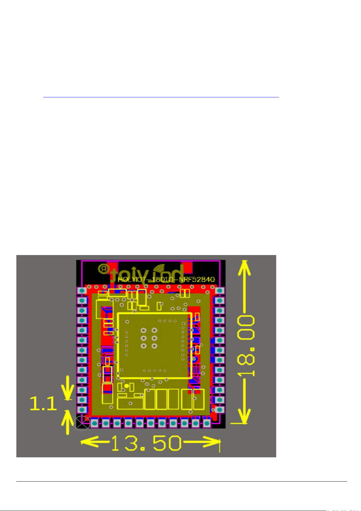
2.1.mechanical drawings
SoftDevices can be programmed in nRF5 series devices, and are freely downloadable from the Nordic website.please download
that here :http://www.nordicsemi.com/eng/nordic/download_resource/60625/19/19221576/116072
Over-The-Air DFU
The SoC is supported by an Over-The-Air Device Firmware Upgrade (OTA DFU) feature. This allows for in the field
updates of application software and SoftDevice.
- 4 -
Page 5
Back
- 5 -
Page 6

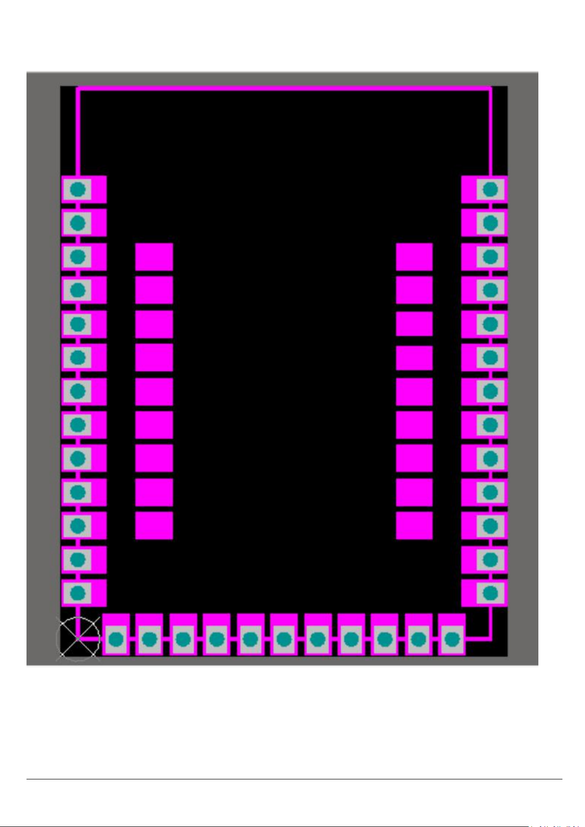
2.2.Pin assignments
PIN# number PIN define Functions
1 GND Ground
2 P1.10 Digital I/O
3 P1.11 Digital I/O
Bottom of the board
Trace data
- 6 -
Page 7

4 P1.13 Digital I/O
5 P1.15 Digital I/O
6 P0.03 Digital I/O
Analog input
7 P0.02 Digital I/O
Analog input
8 P0.28 Digital I/O
Analog input
9 P0.29 Digital I/O
Analog input
10 P0.30 Digital I/O
Analog input
11 P0.31 Digital I/O
Analog input
12 P0.04 Digital I/O
Analog input
13 P0.05 Digital I/O
Analog input
14 P1.14 Digital I/O
15 P1.12 Digital I/O
16 P0.25 Digital I/O
17 P0.11 Digital I/O
18 P1.08 Digital I/O
19 P0.27 Digital I/O
20 P0.08 Digital I/O
21 P0.06 Digital I/O
22 P0.26 Digital I/O
23 P1.07 Digital I/O
24 P1.05 Digital I/O
25 P0.24 Digital I/O
26 P0.20 Digital I/O
27 P0.17 Digital I/O
28 P0.15 Digital I/O
29 P0.14 Digital I/O
30 P0.13 Digital I/O
31 P0.16 Digital I/O
32 GND Ground
33 P0.10 Digital I/O
NFC input
34 P0.09 Digital I/O
NFC input
35 P1.06 Digital I/O
- 7 -
Page 8

36 P1.04 Digital I/O
3. Mounting our board on the host PCBA
37 SWDIO SWD for debug and programming
38 SWDCLK SWD for debug and programming
39 P1.02 Digital I/O
40 P1.01 Digital I/O
41 P1.03 Digital I/O
42 P1.00 Digital I/O
43 P0.22 Digital I/O
44 GND Ground
45 D+ Digital I/O
46 D- Digital I/O
47 VBUS Power
48 P0.18 Digital I/O
49 P0.19 Digital I/O
50 P0.21 Digital I/O
51 P0.23 Digital I/O
52 P0.12 Digital I/O
Trace data
53 P1.09 Digital I/O
Trace data
54 P0.07 Digital I/O
Trace clock
55 V_nRF(VDD/VDDH) VDD/VDDH
We suggest that you mounting our RF board(Holyiot-18010_nRF52840) on the board , something like that .
1 . for the best Bluetooth performance , the antenna of the area need to extends about several mml without ground under the
antenna of the edge of the host PCB
2 . the next choise is that place our board at the corner of host PCB , the antenna of board need to extends several mm
outside of the Ground plane of the host PCB
- 8 -
Page 9

4. Miscellaneous
Soldering Temperature-Time Profile for Re-Flow Soldering
Maximum number of cycles for re-flow is 2. No opposite side re-flow is allowed due to module weight.
- 9 -
Page 10

5. Absolute maximum ratings
Maximum ratings are the extreme limits to which the chip can be exposed for a limited amount of time
without permanently damaging it. Exposure to absolute maximum ratings for prolonged periods of time may
affect the reliability of the device.
Absolute maximum ratings
- 10 -
Page 11

- 11 -
Page 12

This device complies with part 15 of the FCC Rules.
Operation is subject to the following two conditions:
(1) This device may not cause harmful interference, and
(2) this device must accept any interference received,
including interference that may cause undesired operation.
Note: This equipment has been tested and found to comply with the limits for a Class
B digital device, pursuant to Part 15 of the FCC Rules. These limits are designed to
provide reasonable protection against harmful interference in a residential installation.
This equipment generates, uses and can radiate radio frequency energy and, if not
installed and used in accordance with the instructions, may cause harmful interference
to radio communications.
However, there is no guarantee that interference will not occur in a particular
installation. If this equipment does cause harmful interference to radio or television
reception, which can be determined by turning the equipment off and on, the user is
encouraged to try to correct the interference by one or more of the following
measures:
Reorient or relocate the receiving antenna.
Increase the separation between the equipment and receiver.
Connect the equipment into an outlet on a circuit different from that to which the
receiver is connected.
Consult the dealer or an experienced radio/TV technician for help.
- 12 -
Page 13

Warning: Changes or modifications to this unit not expressly approved by the part
responsible for compliance could void the user's authority to operate the equipment.
FCC Radiation Exposure Statement
This equipment complied with FCC radiation exposure limits set forth for an uncontrolled
environment. This equipment should be installed and operated with minimum distance 20cm
between the radiator & your body.
- 13 -
Page 14

7. contact us
Shenzhen holyiot technology Co.,LTD
Rm.308, 310, Bldg 9. Wangtang industrial Park xinwei Vil., xili Town. Nanshan Dist, Shenzhen China.
TEL:+8615220262142
Email: spring@hyyunjia.com
Website :www.hyyunjia.com/www.holyiot.com
- 14 -
Page 15

IMPORTANT NOTE:
This module is intended for OEM integrator only and the OEM integrators and instructed to
ensure that the end user has no manual instructions to remove or install the device. The OEM
integrator is still responsible for the FCC compliance requirement of the end product, which
integrates this module.
Integration is typically strictly restricted to Grantee himself or dedicated OEM integrators under
control of the Grantee.
In the event that these conditions can not be met (for example certain laptop configurations or
co-location with another transmitter. then the FCC authorization is no longer considered valid
and the FCC ID can not be used on the final product. In these circumstances, the OEM
integrator will be responsible for re-evaluating the end product (including the transmitter) and
obtaining a separate FCC authorization.
The module will be responsible to satisfy SAR/RF Exposure requirements, when the module
integrated into any (portable, mobile, fixed) host device.
The module must in the end-product be installed in such manner that the authorized antennas
can be used, any change of the antenna will void the certification.
LABEL OF THE END PRODUCT:
The final end product must be labelled in a visible area with the following "Contains TX FCC ID:
2ALGY-NRF52840
If the size of the end product
is smaller than 8x10cm, then additional FCC
part 15.19 statement is required to be available in the users manual: This device complies with
Part 15 of the FCC Rules. Operation is subject to the following two conditions: (1) this device
may not cause harmful interference, and (2) this device must accept any interference received,
including interference that may cause undesired operation.
 Loading...