


HTG2150
Preliminary
8-Bit 320 Pixel LCD Microcontroller
Features
Operating voltage: 2.2V~3.6V
·
16K ´ 16 bits program ROM
·
192 ´ 8 bits data RAM
·
8~12 bidirectional I/O lines
·
8 common ´ 33~40 segment LCD driver
·
One 16-bit programmable timer
·
with overflow interrupts
One 8-bit programmable timer with 8 stage
·
prescaler for PFD
One 8-bit programmable timer with 8 stage
·
prescaler for Time base
One 8-bit PWM audio output to directly
·
drive speaker and buzzer
General Description
The HTG2150 is an 8-bit high performance
RISC-like microcontroller. The single cycle in
struction and two-stage pipeline architecture
make it suitable for high speed application. The
device is ideally suited for multiple LCD low
Watchdog Timer
·
On-chip RC oscillator for system clock and
·
32768Hz crystal oscillator for timebase and
LCD driver
HALT function and wake-up feature reduce
·
power consumption
8-level subroutine nesting
·
Bit manipulation instructions
·
63 powerful instructions
·
One interrupt input
·
power application among which are calcula
tors, clock timer, game, scales, toys and hand
held LCD products, as well as for battery sys
tems.
-
-
1 July 24, 2000
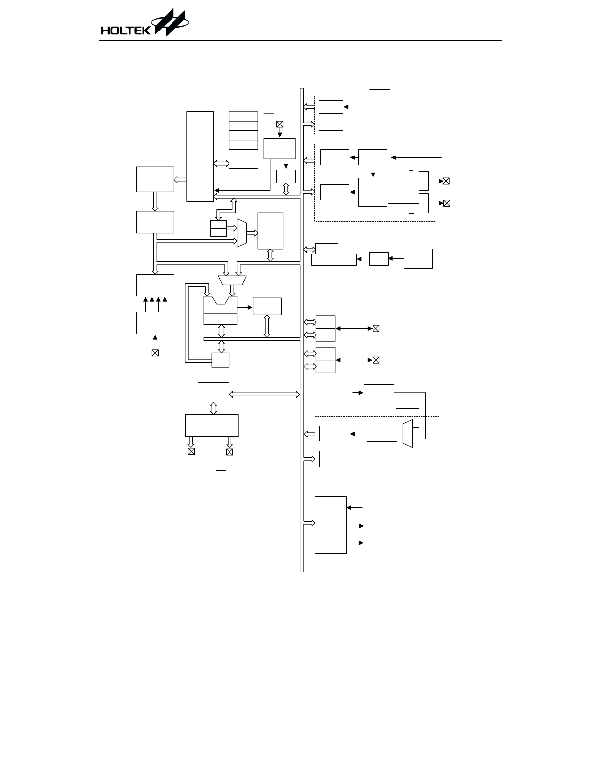
Block Diagram
Preliminary
SYS CLK/4
HTG2150
Program
ROM
Instruction
R egister
Instruction
D ecoder
Tim ing
G enerator
OSCI
RES
VDD
VSS
Program
C ounter
Memory
MP0
MP1
Shifter
ACC
LC D
ALU
STACK0
STACK1
STACK2
STACK3
STACK4
STACK5
STACK6
STACK7
MUX
M
U
X
IN T /S E G 3 7
In te rru p t
DATA
Memory
STATUS
Circuit
IN T C
TM R0
TM R0C
16 bit
TM R2
TM R2C
WDTS
W D T P rescaler
PAC
PORT A
PA
PBC
PORT B
PB
SYS C LK
32768H z Crystal
8-stage
P resca ler
PW M D AC1
PFD
PW M D AC2
256
¸
PA0~PA7
PB4~PB7/SEG 33~SEG36
8-stage
P resca ler
M
U
X
M
U
X
WDT RC
OSC
SYS C LK
PW M 1
PW M 2
LCD Driver
COM 0~CO M 7
SEG0~SEG 32
PB4~PB7/SEG 33~SEG36
IN T /S E G 3 7
XOUT/SEG 38
XIN/SEG 39
TM R3
TM R3C
PW M
D/A
8-stage
P resca ler
SYS CLK
PW M D AC1
PW M D AC2
M
U
X
2 July 24, 2000
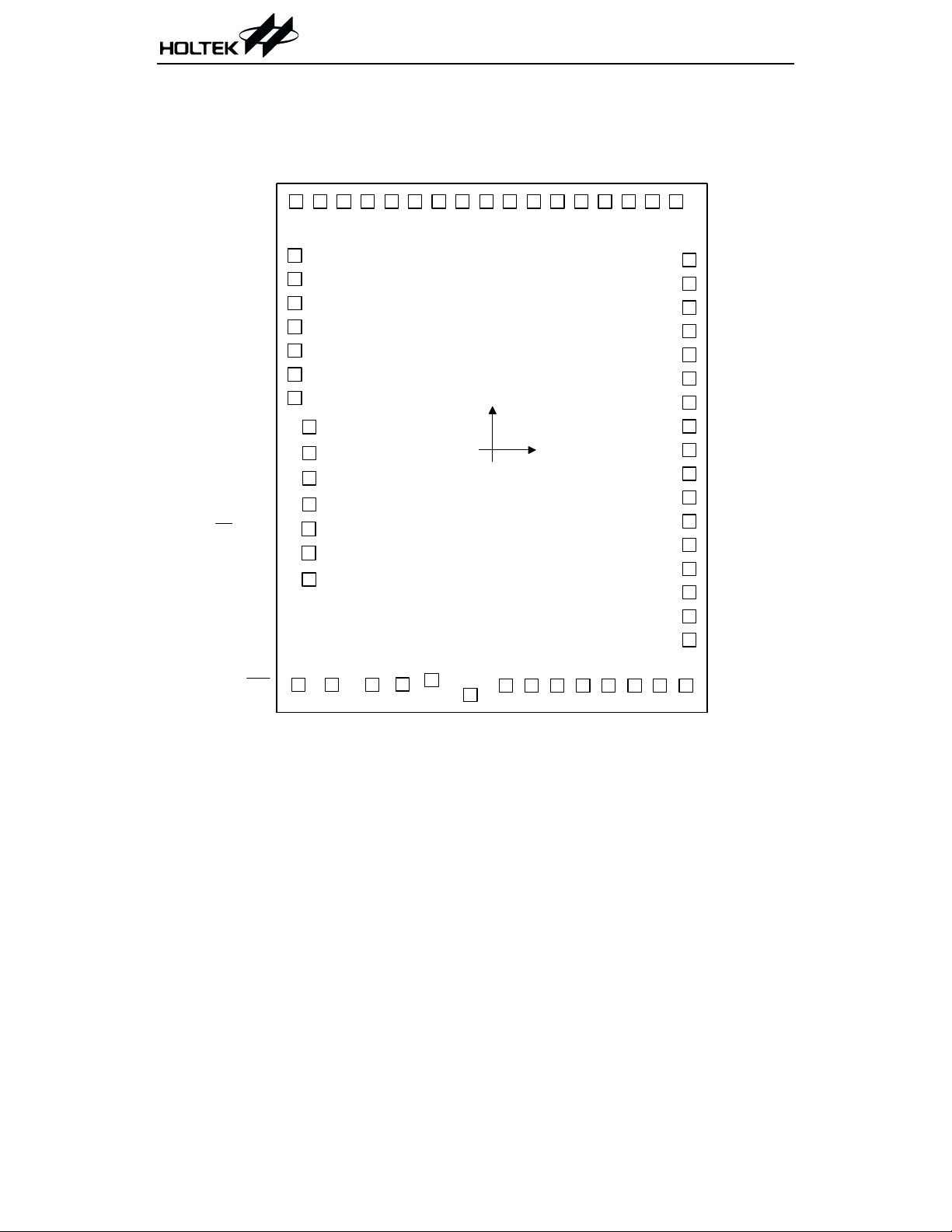
Pad Assignment
Preliminary
SEG 10
SEG 11
SEG 12
SEG 13
SEG 14
SEG 15
SEG 16
SEG 17
SEG 18
SEG 19
SEG 20
SEG 21
SEG 22
SEG 23
SEG 24
HTG2150
SEG 9
SEG 25
SEG 26
SEG 27
SEG 28
SEG 29
SEG 30
SEG 31
SEG 32
PB4/SEG 33
PB5/SEG 34
PB6/SEG 35
PB7/SEG 36
IN T /S E G 3 7
XOUT/SEG 38
XIN/SEG 39
51
59
60
61
62
1
2
3
4
5
6
7
8
9
10
11
12
13
14
15
(0 ,0 )
52
50
48
49
47
46
SEG 8
45
SEG 7
44
SEG 6
43
SEG 5
42
SEG 4
SEG 3
41
40
SEG 2
39
SEG 1
38
SEG 0
COM 7
37
36
COM 6
COM 5
35
COM 4
34
COM 3
33
COM 2
32
31
COM 1
30
COM 0
RES
18
17
16
PW M 1
PW M 2
20
19
OSCI
VDD
22532354245525562657275828
21
PA0
PA1
PA2
VSS
PA3
PA4
PA5
29
PA6
PA7
* The IC substrate should be connected to VSS in the PCB layout artwork.
3 July 24, 2000

Preliminary
HTG2150
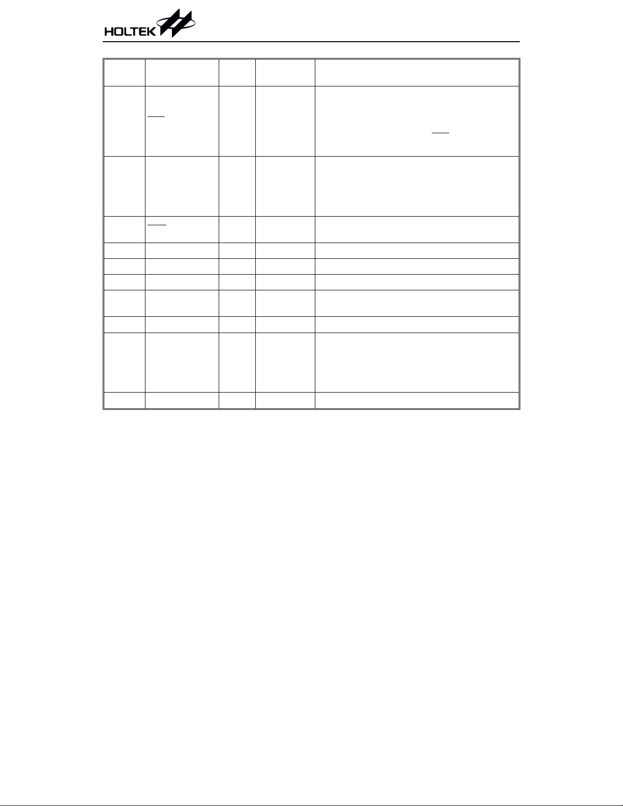
Pad Coordinates
Pad No. X Y Pad No. X Y
1
2
3
4
5
6
7
8
9
10
11
12
13
14
15
16
17
18
19
20
21
22 58.61
23 175.41
24 289.41
25 406.21
26 520.21
27 637.01
28 751.01
29 867.81
30 882.36
31 882.36
-880.45
-887.11
-887.11
-887.11
-887.11
-887.11
-887.11
-887.11
-822.70
-822.70 -13.52
-822.70 -127.52
-822.70 -244.52
-824.04 -354.49
-824.04 -462.62
-823.97 -580.52
-871.13 -1052.80
-720.90 -1052.80
-539.25 -1052.80
-404.50 -1051.65
-273.79 -1032.67
-99.06 -1097.34
1114.46 32 882.36
872.13 33 882.36
765.63 34 882.36
659.03 35 882.36
552.53 36 882.36
445.93 37 882.36
339.43 38 882.36
232.83 39 882.36 106.43
103.48 40 882.36 212.93
-1057.70
-1057.70
-1057.70
-1057.70
-1057.70
-1057.70
-1057.70
-1057.70
-852.57
-745.97
41 882.36 319.53
42 882.36 426.03
43 882.36 532.63
44 882.36 639.13
45 882.36 745.73
46 882.36 852.23
47 824.35 1114.46
48 717.85 1114.46
49 611.25 1114.46
50 504.75 1114.46
51 398.15 1114.46
52 291.65 1114.46
53 185.05 1114.46
54 78.55 1114.46
55
56
57
58
59
60
61
62
-28.05
-134.55
-241.15
-347.65
-454.25
-560.75
-667.35
-773.85
Unit: mm
-639.47
-532.87
-426.37
-319.77
-213.27
-106.67
-0.17
1114.46
1114.46
1114.46
1114.46
1114.46
1114.46
1114.46
1114.46
Pad Description
Pad No. Pad Name I/O
38~62
1~8
9~12
SEG0~SEG24
SEG25~SEG32
PB4~PB7/
SEG33~SEG36
O
I/O
or
O
Mask
Option
¾
Input/Output
or Segment
Output
Description
LCD segment signal output.
Selectable as bidirectional input/output or LCD
segment signal output by mask option. On
bidirectional input/output port. Software instruc
tions determine the CMOS output or schmitt trig
ger input with pull-high resistor. PB4~PB7 share
pad with SEG33~SEG36.
4 July 24, 2000
-
-
Preliminary
HTG2150
Pad No. Pad Name I/O
I
13 INT
15
14
16 RES
17 PWM1 O CMOS Positive PWM CMOS output
18 PWM2 O CMOS Negative PWM CMOS output
19 VDD
20 OSCI I
21 VSS
22~29 PA0~PA7 I/O
37~31 COM7~COM0 O
/SEG37
XIN/SEG39
XOUT/SEG38
or
O
IorO
O
I
¾¾
¾¾
Mask
Option
Interrupt
input or
Segment 37
output
Crystal or
Segment
Output
¾
¾
Wake-up
or None
Wake-up
¾
Description
Selectable as external interrupt schmitt trigger
input or LCD segment 37 signal output by mask
option. External interrupt schmitt trigger input
with pull-high resistor. Edge triggered activated
on a high to low transition. INT
SEG37.
Selectable as 32768Hz crystal oscillator or LCD
segment signal output by mask option. Crystal
oscillator (32.768kHz) for Timer 3 and LCD
clock. XIN shares pad with SEG39; XOUT
shares pad with SEG38.
Schmitt trigger reset input. Active low without
pull-high resistor.
Positive power supply
OSCI is connected to the RC network of the in
ternal system clock.
Negative power supply, ground
Bidirectional 8-bit input/output port. Each bit
can be configured as a wake-up input by mask
option. Software instructions determine the
CMOS output or schmitt trigger input with
pull-high resistor.
LCD common signal output
shares pad with
-
Absolute Maximum Ratings
Supply Voltage ..............................-0.3V to 3.6V
Input Voltage .................V
Note: These are stress ratings only. Stresses exceeding the range specified under ²Absolute Maxi
mum Ratings² may cause substantial damage to the device. Functional operation of this device
at other conditions beyond those listed in the specification is not implied and prolonged expo
sure to extreme conditions may affect device reliability.
-0.3V to VDD+0.3V
SS
Storage Temperature.................-50°Cto125°C
Operating Temperature ..................0°Cto70°C
5 July 24, 2000
-
-
Preliminary
HTG2150
D.C. Characteristics
Symbol Parameter
V
I
DD
I
STB1
I
STB2
V
V
V
V
V
V
I
OH1
I
OH2
I
OH3
I
OL1
I
OL2
I
OL3
R
DD
IL1
IH1
IL2
IH2
IL3
IH3
PH
Operating Voltage
Operating Current (RC OSC) 3V
Standby Current With 7mA LCD Bias
Option (RTC ON, LCD ON)
Standby Current LCD Bias Off Option
(RTC ON, LCD OFF)
Input Low Voltage for PA/PB 3V
Input High Voltage for PA/PB 3V
Input Low Voltage (INT)3V¾0
Input High Voltage (INT)3V¾2.3
Input Low Voltage (RES)3V
Input High Voltage (RES)3V
Port A, Port B Source Current 3V
Segment, Common Output Source
Current
PWM1/PWM2 Source Current 3V
Port A, Port B Sink Current 3V
Segment, Common Output
Sink Current
PWM1/PWM2 Sink Current 3V
Pull-high Resistance of PA/PB and INT 3V
Test Conditions
V
Conditions
DD
¾¾
No load,
=4MHz
f
SYS
No load,
3V
HALT mode
No load,
3V
HALT mode
¾
¾
¾¾
¾¾
V
=2.7V
OH
=2.7V
V
3V
OH
V
=2.7V
OH
V
=0.3V
OL
=0.3V
V
3V
OL
V
=0.3V
OH
¾
Ta=25°C
Min. Typ. Max. Unit
2.2
¾
¾¾
¾¾
0
2.1
-1 -2 ¾
3.6 V
¾
12mA
20
mA
5
mA
0.9 V
¾
3V
¾
0.7 V
¾
3V
¾
1.5
2.4
¾
¾
V
V
mA
-50 -90 ¾mA
-8 -10 ¾
1.5 4
80 130
12 16
40 60 80
mA
mA
¾
¾mA
mA
¾
kW
A.C. Characteristics
Symbol Parameter
f
SYS
t
RES
t
SST
t
INT
Note: t
System Clock (RC OSC)
External Reset Low Pulse Width
System Start-up Timer Period
Interrupt Pulse Width
=1/f
SYS
SYS
Test Conditions
V
DD
3V
Conditions
¾
¾
2.2V
¾
¾¾
Power-up or
¾
Wake-up from HALT
¾¾
6 July 24, 2000
Min. Typ. Max. Unit
400
400
400
1
¾
1
4000
¾
2000
¾
1000
¾
¾¾ms
1024
¾
¾¾ms
Ta=25°C
kHz2.4V
t
SYS
Preliminary
Functional Description
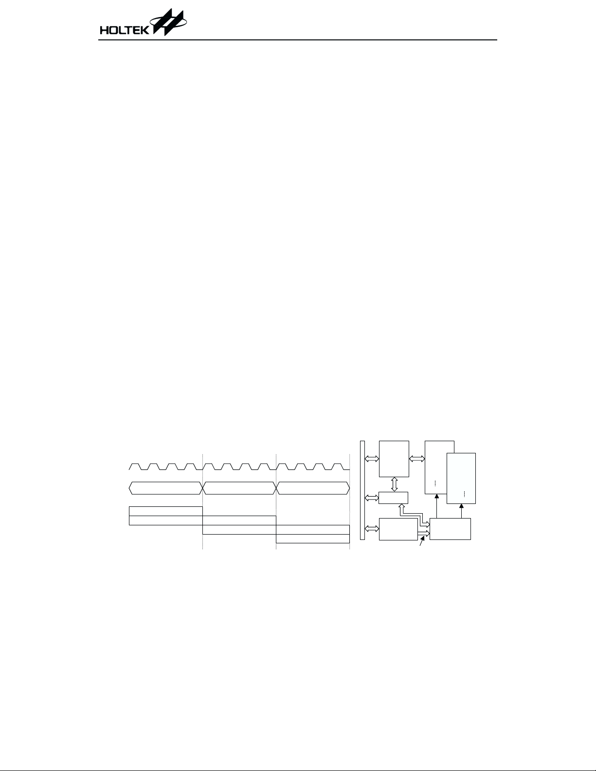
Execution flow
The system clock for the HTG2150 is derived
from an RC oscillator. The system clock is inter
nally divided into four non-overlapping clocks.
One instruction cycle consists of four system
clock cycles.
Instruction fetching and execution are pipelined in
such a way that a fetch takes one instruction cycle
while decoding and execution takes the next in
struction cycle. However, the pipelining scheme
causes each instruction to effectively execute in one
cycle. If an instruction changes the program coun
ter, two cycles are required to complete the instruc
tion.
Program counter - PC
The 13-bit program counter (PC) controls the
sequence in which the instructions stored in the
program ROM are executed and its contents
specify a maximum of 8192 addresses.
After accessing a program memory word to
fetch an instruction code, the contents of the
program counter are incremented by one. The
program counter then points to the memory
word containing the next instruction code.
When executing a jump instruction, conditional
skip execution, loading PCL register, subroutine call, initial reset, internal interrupt, external interrupt or return from subroutine, the PC
manipulates the program transfer by loading
the address corresponding to each instruction.
T1 T2 T3 T4 T1 T2 T3 T4 T1 T2 T3 T4
System
Clock
PC
PC PC+1 PC+2
F e tc h IN S T (P C )
Execute IN S T (PC -1)
F e tc h IN S T ( P C + 1 )
Execute IN S T (PC )
Execution flow
The conditional skip is activated by instruction.
Once the condition is met, the next instruction,
fetched during the current instruction execu
-
tion, is discarded and a dummy cycle replaces it
to get the proper instruction. Otherwise pro
ceed with the next instruction.
The lower byte of the program counter (PCL) is
a readable and writeable register (06H).
Moving data into the PCL performs a short
jump. The destination will be within 256 loca
tions.
When a control transfer takes place, an addi
tional dummy cycle is required.
-
-
Program memory - ROM
The program memory, which contains execut
able program instructions, data and table infor
mation, is composed of a 16384 x 16 bit format.
However as the PC (program counter) is com
prised of only 13 bits, the remaining 1 ROM ad
dress bit is managed by dividing the program
memory into 2 banks, each bank having a range
between 0000H and 1FFFH. To move from the
present ROM bank to a different ROM bank,
the higher 1 bit of the ROM address are set by
the BP (Bank Pointer), while the remaining 13
bits of the PC are set in the usual way by executing the appropriate jump or call instruction.
As the full 14 address bits are latched during
the execution of a call or jump instruction, the
correct value of the BP must first be setup before a jump or call is executed. When either a
software or hardware interrupt is received,
note that no matter which ROM bank the pro-
Bank0
0000H
1FFFH
R O M Address
A13 bit Latch
F e tc h IN S T (P C + 2 )
Execute INST (PC +1)
13 bits
Program
C ounter
Stack
Bank Pointer
R egister Bit5
Latch data on E xecution of Jum p or C all Instruction
16K Program R O M Addressing Architecture
HTG2150
Bank1
16
8192
´
Bits
2000H
3FFFH
-
-
-
-
-
-
-
-
7 July 24, 2000
Preliminary
HTG2150
gram is in the program will always jump to the
appropriate interrupt service address in Bank
0. The original full 14 bit address will be stored
on the stack and restored when the relevant
RET/RETI instruction is executed, automati
cally returning the program to the original
ROM bank. This eliminates the need for pro
grammers to manage the BP when interrupts
occur.
Certain locations in Bank 0 of program memory
are reserved for special usage:
·
ROM Bank 0 (BP5~BP7=000B)
The ROM bank 0 ranges from 0000H to
1FFFH.
·
Location 000H
This area is reserved for the initialization
program. After chip reset, the program al
·
Location 008H
This area is reserved for the timer counter 0 in
terrupt service program. If a timer interrupt re
sults from a timer counter 0 overflow, and if the
-
interrupt is enabled and the stack is not full,
the program begins execution at location 008H.
-
0000H
0004H
0008H
000C H
010H
014H
018H
-
D evice initialization program
External interrupt subroutine
Tim er counter 0 interrupt subroutine
U nused
Tim er 2 interrupt subroutine
Tim er 3 interrupt subroutine
D /A buffer em pty interrupt
Program
ROM
ways begins execution at location 000H.
·
Location 004H
This area is reserved for the external inter
rupt service program. If the INT
input pin is
activated, and the interrupt is enabled and
the stack is not full, the program begins exe
cution at location 004H.
Mode
*13 *12 *11 *10 *9 *8 *7 *6 *5 *4 *3 *2 *1 *0
-
3FFFH
-
Program Rom Address
16 bits
Program memory
Initial reset 0 0 0 0 0 0 0 0 0 0 0 0 0 0
External interrupt 0 0 0 0 0 0 0 0 0 0 0 1 0 0
Timer counter 0 overflow 0 0 0 0 0 0 0 0 0 0 1 0 0 0
Timer 2 overflow 0 0 0 0 0 0 0 0 0 1 0 0 0 0
Timer 3 overflow 0 0 0 0 0 0 0 0 0 1 0 1 0 0
D/A buffer empty interrupt 0 0 0 0 0 0 0 0 0 1 1 0 0 0
Skip PC+2
Loading PCL *13 *12 *11 *10 *9 *8 @7 @6 @5 @4 @3 @2 @1 @0
Jump, call branch BP.5 #12 #11 #10 #9 #8 #7 #6 #5 #4 #3 #2 #1 #0
Return from subroutine S13 S12 S11 S10 S9 S8 S7 S6 S5 S4 S3 S2 S1 S0
-
-
Note: *13~*0: Program ROM address
@7~@0: PCL bits
#12~#0: Instruction code bits
Program rom address
S13~S0: Stack register bits
BP.5: Bit 5 of bank pointer (04H)
8 July 24, 2000

Preliminary
HTG2150
·
Location 010H/014H
This area is reserved for the timer 2/3 interrupt
service program. If a timer interrupt results
from a timer 2/3 overflow, and if the interrupt is
enabled and the stack is not full, the program
begins execution at location 010H/014H.
·
Location 018H
This area is reserved for the D/A buffer empty
interrupt service program. After the system
latch a D/A code at RAM address 28H, the in
terrupt is enable, and the stack is not full, the
program begins execution at location 020H.
·
Location 020H
For best condition, this is the starting loca
tion for writing the program..
·
ROM Bank 1 (BP5~BP7=001B)
The range of the ROM starts from 2000H to
3FFFH.
·
Table location
Any location in the ROM space can be used as
look up tables. The instructions TABRDC [m]
(use for any bank) and TABRDL [m] (only
used for last page of program ROM) transfers
the contents of the lower-order byte to the
specified data memory, and the higher-order
byte to TBLH (08H). Only the destination of
the lower-order byte in the table is
well-defined. The higher-order byte of the table word are transferred to the TBLH. The table higher-order byte register (TBLH) is read
only. The table pointer (TBHP, TBLP) is a
read/write register (1FH, 07H), which indicates the table location. Before accessing the
table, the location must be placed in TBLP.
The TBLH is read only and cannot be restored. If the main routine and the ISR (Inter
rupt Service Routine) both employ the table
read instruction, the contents of the TBLH in
the main routine are likely to be changed by
the table read instruction used in the ISR. Er
rors can occur. In other words, using the table
read instruction in the main routine and the
ISR simultaneously should be avoided. How
ever, if the table read instruction has to be ap
plied in both the main routine and the ISR,
the interrupt is supposed to be disabled prior
to the table read instruction. It will not be en
-
-
-
abled until the TBLH has been backed up. All
table related instructions need two cycles to
complete the operation. These areas may
function as normal program memory depend
ing upon the requirements.
Stack register - STACK
This is a special part of the memory which is
used to save the contents of the program coun
ter (PC) only. The stack is organized into eight
levels and is neither part of the data nor part of
the program space, and is neither readable nor
writeable. The activated level is indexed by the
stack pointer (SP) and is neither readable nor
writeable. At a subroutine call or interrupt ac
knowledgment, the contents of the program
counter and ROM address A13 bit latch Data
are pushed onto the stack. At the end of a subroutine or an interrupt routine, signaled by a
return instruction (RET or RETI), the program
counter and ROM address A13 bit latch Data
are restored to its previous value from the
stack. After a chip reset, the SP will point to the
top of the stack.
If the stack is full and a non-masked interrupt
takes place, the interrupt request flag will be recorded but the acknowledgment will be inhibited.
When the stack pointer is decremented (by RET
or RETI), the interrupt will be serviced. This fea
ture prevents stack overflow allowing the pro
-
-
-
-
-
-
-
-
-
Instruction(s)
TABRDC [m] #5 #4 #3 #2 #1 #0 @7 @6 @5 @4 @3 @2 @1 @0
TABRDL [m] 1 1 1 1 1 1 @7 @6 @5 @4 @3 @2 @1 @0
Note: @7~@0: TBLP register bit 7~bit 0
#5~#0: TBHP register bit 13~bit 8
*13 *12 *11 *10 *9 *8 *7 *6 *5 *4 *3 *2 *1 *0
Table Location
Table location
*13~*0: Current Program ROM table
address bit 13~bit 0
9 July 24, 2000
Preliminary
HTG2150
grammer to use the structure more easily. In a
similar case, if the stack is full and a CALL is
subsequently executed, stack overflow occurs and
the first entry will be lost (only the most recent
eight return address are stored).
00H
IA R 0
01H
MP0
02H
IA R 1
03H
MP1
04H
BP
05H
ACC
06H
PCL
07H
TBLP
08H
TBLH
09H
WDTS
STATUS
0AH
IN T C
0BH
TM R 0H
0C H
TM R 0L
0D H
TM R 0C
0EH
0FH
10H
11H
PA
12H
PAC
13H
PB
14H
PBC
15H
16H
17H
18H
19H
1AH
1BH
1C H
1D H
IN T C H
1EH
TBH P
1FH
20H
TM R 2
21H
TM R 2C
22H
23H
TM R 3
24H
TM R 3C
25H
X'TALC
26H
PW M C
27H
28H
PW M
29H
2AH
2BH
2C H
2D H
LC D C LC D C ontrol R egister
2EH
COM R
2FH
30H
3FH
40H
FFH
80H
A7H
Indirect Addressing R egister 0
M em ory P ointer 0
Indirect Addressing R egister 1
M em ory P ointer 1
Bank P ointer
A ccum ulato r
Program C ounter Lower-byte R egister
Table Pointer Low er-order Byte R egister
Table H igher-order Byte R egister
W atchdog Tim er O ption Setting R egister
Status R egister
Interrupt C ontrol R egister
Tim er C ounter 0 H igher-order B yte R egister
Tim er C ounter 0 Low er-order B yte R egister
Tim er C ounter 0 C ontrol R egister
PA I/O D ata R egister
PA I/O C ontrol R egister
PB I/O D ata R egister
PB I/O C ontrol R egister
Interrupt C ontrol H igher-order Byte R egister
Table Pointer H igher-order B yte R egister
Tim er 2 R egister
Tim er 2 C ontrol R egister
Tim er 3 R egister
Tim er 3 C ontrol R egister
X 'tal Fa st O scilla tor up C ontrol
PW M C ontrol
PW M Data
C om m on P ad A ddress R otator
G eneral Purpose
Bank 0 D ata M em ory
(192 B yte)
Bank 15 D ata M em ory
(40 B yte)
S p e c ia l P u rp o s e
D ata M em ory
: U n u s e d
R ead as "00"
PB bit 3/2/1/0 R ead=0
RAM mapping
Data memory - RAM
·
Bank 0 (BP4~BP0=00000)
The Bank 0 data memory includes special
purpose and general purpose memory. The
special purpose memory is addressed from
00H to 2FH, while general purpose memory is
addressed from 40H to FFH. All data memory
areas can handle arithmetic, logic, increment,
decrement and rotate operations directly. Ex
cept for some dedicated bits, each bit in the
data memory can be set and reset by the SET
[m].i and CLR [m].i instructions, respectively.
They are also indirectly accessible through the
memory pointer registers (MP0;01H, MP1;03H).
·
Bank 15 (BP4~BP0=01111B)
The range of RAM starts from 80H to A7H.
On the LCD, every bit stands for one dot. If
the bit is ²1², the light of the dot on the LCD
will be turned on. If the bit is ²0², then it will
be turned off. Only MP1 can deal with the
memory of this range.
The contrast form of RAM location, COM
MON, and SEGMENT is as follows.
Indirect addressingregister
Location 00H and 02H are indirect addressing
registers that are not physically implemented.
Any read/write operation of [00H] and [02H] access data memory are pointed to by MP0 (01H)
and MP1 (03H) respectively. Reading location
00H or 02H indirectly will return the result 00H.
Writing indirectly results in no operation.
The function of data movement between two indirect addressing registers, is not supported. The
memory pointer registers, MP0 and MP1, are
8-bit registers which can be used to access the
data memory by combining corresponding indi
rect addressing registers but Bank 15 can use
MP1 only.
Accumulator
The accumulator is closely related to ALU oper
ations. It is also mapped to location 05H of the
data memory and it can carry out immediate
data operations. The data movement between
two data memories has to pass through the ac
cumulator.
-
-
-
-
-
10 July 24, 2000
Preliminary
HTG2150
LCD driver output
The maximum output number of the HTG2150
LCD driver is 8´40. The LCD driver bias type is
²R²type, no external capacitor is required and the
bias voltage is 1/4 bias. Some of the Segment out
puts share pins with another pins, PB4~PB7
(SEG33~SEG36), INT
(SEG37), XOUT (SEG38),
XIN (SEG39). Whether segment output or I/O pin
can individually bedecided bymask option.
32H z
COM 0
COM 1
SEG 0
512H z
3/4 V
2/4 V
1/4 V
GND
3/4 V
2/4 V
1/4 V
GND
3/4 V
2/4 V
1/4 V
GND
3
2
1
V
DD
DD
DD
DD
V
DD
DD
DD
DD
V
DD
DD
DD
DD
6
8
4
7
5
LCD driver output can be enabled or disabled by
setting the LCD (bit 6 of LCDC; 2EH) without the
influence of the related memory condition. There
is a special function for LCD display, which is Ro
tate function. There are 8 kinds of Rotate func
tion, (user can changethe dataof theSS0 toSS3.)
An example of an lcd driving waveform (1/8
duty, 1/4 bias) is shown below.
3
2
1
6
8
4
7
5
3
4
2
1
5
-
-
LC D d isplay m em ory: (B ank 15)
Address
COM 0
COM 1
COM 2
COM 3
COM 4
COM 5
COM 6
COM 7
80H
Bit0
Bit1
Bit2
Bit3
Bit4
Bit5
Bit6
Bit7
SEG 0
81H
SEG 1
82H
SEG 2
83H
SEG 3
84H
SEG 4
85H
SEG 5
SEG 17
91H
92H
SEG 18
11 July 24, 2000
A7H
SEG 39
Preliminary
Register Bit No. Label Function
0~5
6 LCD Control the LCD output (0=disable; 1=enabled) (Default=1)
LCDC
7RC
Can R/W (Default 000000B)
¾
LCD clock source select (Default=0)
1= 32768Hz crystal
0= system clock
LCDC register
HTG2150
Rotate
SSL3 SSL2 SSL1 SSL0
x000
x001
x010
x011
x100
x101
x110
x111
Description
The Pad of common 0 is connected to common 0 and the Pad of common
1 is connected to common 1 and so on.
The Pad of common 0 is connected to common 1 and the Pad of common
1 is connected to common 2 and so on.
The Pad of common 0 is connected to common 2 and the Pad of common
1 is connected to common 3 and so on.
The Pad of common 0 is connected to common 3 and the Pad of common
1 is connected to common 4 and so on.
The Pad of common 0 is connected to common 4 and the Pad of common
1 is connected to common 5 and so on.
The Pad of common 0 is connected to common 5 and the Pad of common
1 is connected to common 6 and so on.
The Pad of common 0 is connected to common 6 and the Pad of common
1 is connected to common 7 and so on.
The Pad of common 0 is connected to common 7 and the Pad of common
1 is connected to common 0 and so on.
2FH register
12 July 24, 2000

Preliminary
HTG2150
Arithmetic and logic unit - ALU
This circuit performs 8-bit arithmetic and logic
operation. The ALU provides the following
functions:
·
Arithmetic operations (ADD, ADC, SUB,
SBC, DAA)
·
Logic operations (AND, OR, XOR, CPL)
·
Rotation (RL, RR, RLC, RRC)
·
Increment and Decrement (INC, DEC)
·
Branch decision (SZ, SNZ, SIZ, SDZ ....)
The ALU not only saves the results of a data op
eration but also changes the status register.
Status register - STATUS
This 8-bit register (0AH) contains the zero flag
(Z), carry flag (C), auxiliary carry flag (AC),
overflow flag (OV), power down flag (PD) and
watchdog time-out flag (TO). It also records the
status information and controls the operation se
quence.
With the exception of the TO and PD flags, bits
in the status register can be altered by instruc
tions like any other register. Any data written
into the status register will not change the TO
or PD flags. In addition it should be noted that
operations related to the status register may
give different results from those intended. The
TO and PD flags can only be changed by system
power up, Watchdog Timer overflow, executing
the HALT instruction and clearing the Watch
dog Timer.
The Z, OV, AC and C flags generally reflect the
status of the latest operations.
In addition, on entering the interrupt sequence
or executing the subroutine call, the status reg
ister will not be automatically pushed onto the
stack. If the contents of status are important
and if the subroutine can corrupt the status
register, precautions must be taken to save it
properly.
Interrupt
The HTG2150 provides an external interrupt and
a PWM D/A interrupt and internal timer inter
rupts. The Interrupt Control register (INTC;0BH,
INTCH;1EH) contains the interrupt control bits to
set the enable/disable and the interrupt request
flags.
Once an interrupt subroutine is serviced, all
other interrupts will be blocked (by clearing the
EMI bit). This scheme may prevent any further
interrupt nesting. Other interrupt requests may
happen during this interval but only the inter-
-
-
-
Labels Bits Function
C is set if the operation results in a carry during an addition operation or if a bor-
C0
AC 1
Z2
OV 3
PD 4
TO 5
¾
row does not take place during a subtraction operation; otherwise C is cleared. C
is also affected by a rotate through carry instruction.
AC is set if the operation results in a carry out of the low nibbles in addition or no
borrow from the high nibble into the low nibble in subtraction; otherwise AC is
cleared.
Z is set if the result of an arithmetic or logic operation is zero; otherwise Z is
cleared.
OV is set if the operation results in a carry into the highest-order bit but not a
carry out of the highest-order bit, or vice versa; otherwise OV is cleared.
PD is cleared when either a system powers up or a CLR WDT instruction is exe
cuted. PD is set by executing the HALT instruction.
TO is cleared by a system power-up or executing the CLR WDT or HALT in
struction. TO is set by a WDT time-out.
6, 7
Undefined bits, read as ²0².
Status register
13 July 24, 2000
-
-
Preliminary
HTG2150
rupt request flag is recorded. If a certain inter
rupt needs servicing within the service routine,
the programmer may set the EMI bit and the
corresponding bit of the INTC to allow interrupt
nesting. If the stack is full, the interrupt request
will not be acknowledged, even if the related in
terrupt is enabled, until the SP is decremented. If
immediate service is desired, the stack must be
prevented from becoming full.
All these kinds of interrupt have a wake-up ca
pability. As an interrupt is serviced, a control
transfer occurs by pushing the program counter
and A13 bit onto the stack followed by a branch
to subroutines at specified locations in the pro
gram memory. Only the program counter and
A13 bit are pushed onto the stack. If the con
tents of the register and Status register
(STATUS) are altered by the interrupt service
program which corrupt the desired control se
quence, the contents should be saved first.
External interrupt is triggered by a high to low
transition of INT
quest flag (EIF; bit 4 of INTC) will be set. When
the interrupt is enabled, and the stack is not
full and the external interrupt is active, a sub
routine call to location 04H will occur. The interrupt request flag (EIF) and EMI bits will be
cleared to disable other interrupts.
The internal timer counter 0 interrupt is initialized by setting the timer counter 0 interrupt
and the related interrupt re
request flag (T0F; bit 5 of INTC), resulting from
a timer 0 overflow. When the interrupt is en
abled, and the stack is not full and the T0F bit
is set, a subroutine call to location 08H will oc
cur. The related interrupt request flag (T0F)
will be reset and the EMI bit cleared to disable
further interrupts.
The Timer 2/3 interrupts are operated in the
same manner as timer 0. While ET2I/ET3I and
T2F/T3F are the related control bits and the re
lated request flags of TMR2/TMR3, which lo
cate at bit0/bit1 and bit4/bi5 of the INTCH
respectively.
During the execution of an interrupt subroutine,
other interrupt acknowledgments are held until
the RETI instruction is executed or the EMI bit
and the related interrupt control bit are set to1(if
the stack is not full). To return from the interrupt
subroutine, the RET or RETI instruction may be
invoked. RETI will set the EMI bit to enable an in
terrupt service, but RET will not.
Interrupts occurring in the interval between
the rising edges of two consecutive T2 pulses,
will be serviced on the latter of the two T2
pulses, if the corresponding interrupts are en
abled. In the case of simultaneous requests the
priorities applied are shown in the following table. These can be masked by resetting the EMI
bit.
-
-
-
-
-
-
Register Bit No. Label Function
Controls the (global) interrupt
(1=enable; 0=disable)
Controls the external interrupt
(1=enable; 0=disable)
Controls the timer counter 0 interrupt
(1=enable; 0=disable)
Unused bit
External interrupt request flag
(1=active; 0=inactive)
Internal timer counter 0 request flag
(1=active; 0=inactive)
Unused bit
INTC register
14 July 24, 2000
INTC
0 EMI
1 EEI
2 ET0I
3
4 EIF
5 T0F
6, 7
¾
¾
Preliminary
Register Bit No. Label Function
Controls the Timer 2 interrupt
(1=enable; 0=disable)
Controls the Timer 3 interrupt
(1=enable; 0=disable)
Internal Timer 2 request flag
(1=active; 0=inactive)
Internal Timer 3 request flag
(1=active; 0=inactive)
INTCH register
INTCH
0 ET2I
1 ET3I
2 PWMI PWM D/A interrupt (1=enable; 0=disable)
3
¾ Should be set as ²0² always
4 T2F
5 T3F
6 PWMF PWM D/A flag (1=active; 0=inactive)
7
¾ Should be set as ²0² always
HTG2150
No. Interrupt Source Priority Vector
a External interrupt 1 04H
Timer counter 0
b
overflow
2 08H
d Timer 2 overflow 4 10H
e Timer 3 overflow 5 14H
f PWM D/A interrupt 6 18H
The timer counter 0 and Timer 2/3 interrupt request flag (T0F/T2F/T3F), External interrupt request flag (EIF), PWM D/A interrupt request flag
(PWMF),Enable Timer 0/2/3 bit (ET0I/ET2I/ET3I)
, Enable PWM D/A interrupt (PWMI), Enable external interrupt bit (EEI) and Enable master interrupt bit (EMI) constitute an interrupt control
register (INTC/INTCH) which is located at
0BH/1EH in the data memory. EMI, EEI, ET0I,
ET2I, ET3I, PWMI are used to control the en
abling/disabling of interrupts. These bits prevent
the requested interrupt from being serviced. Once
the interrupt request flags (T0F, T2F, T3F, EIF,
PWMF) are set, they will remain in the
INTC/INTCH register until the interrupts are ser
viced or cleared by a software instruction.
It is recommended that a program does not use
the ²CALL subroutine² within the interrupt
subroutine. Interrupts often occur in an unpre
dictable manner or need to be serviced immedi
ately in some applications. If only one stack is left
and enabling the interrupt is not well controlled,
the ²CALL subroutine² should not operate in the in
terrupt subroutine as it will damage the original
control sequence.
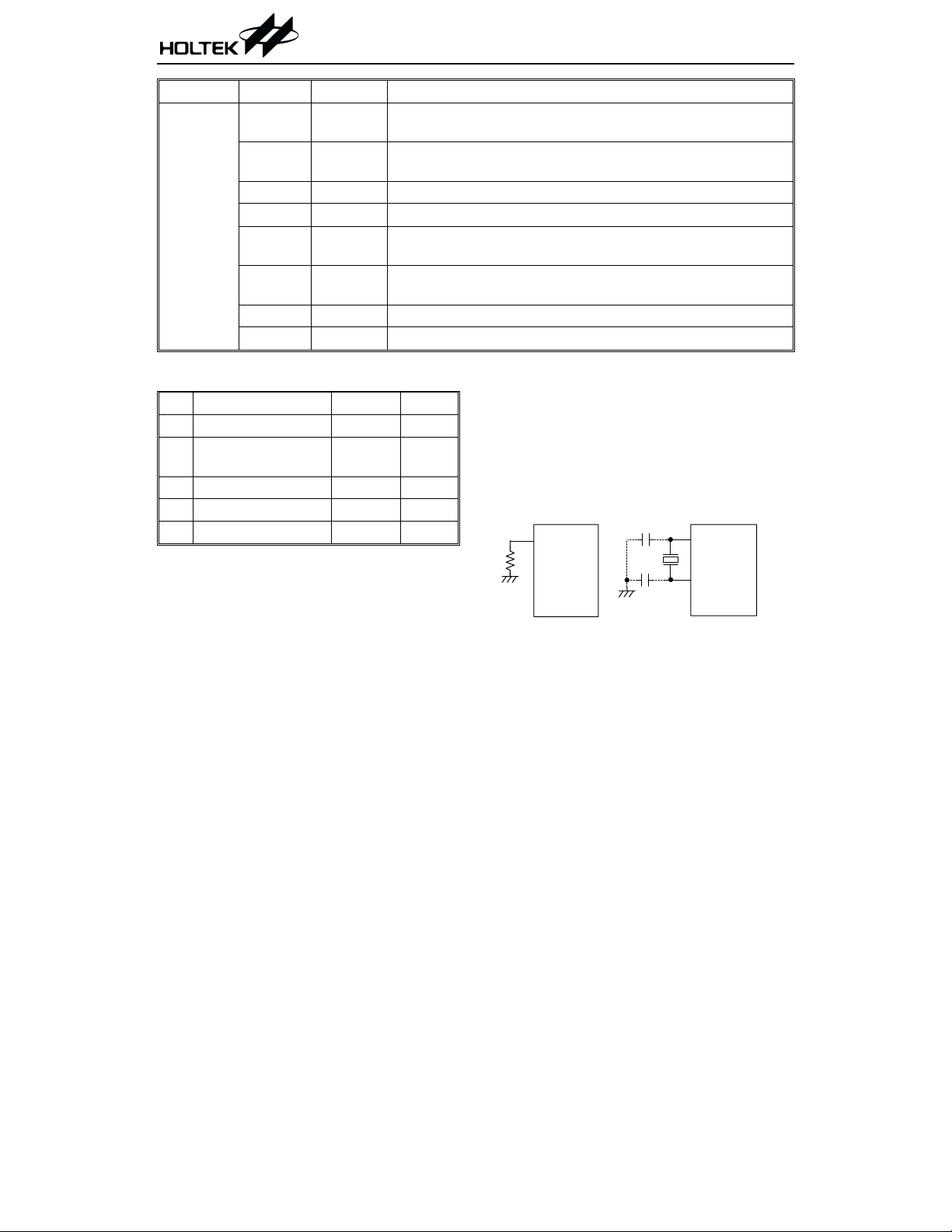
Oscillator configuration
There are two oscillator circuits in the HTG2150.
OSCI
32768H z
R C O scillator
XIN
XOUT
R T C O s c illa to r
System and RTC oscillator
The RC oscillator signal provides the internal
system clock. The HALT mode stops the system
oscillator and ignores any external signal to
conserve power. Only the RC oscillator is de
signed to drive the internal system clock. The
RTC oscillator provides the Timer 3 and LCD
driver clock source.
The RC oscillator needs an external resistor
connected between OSCI and VSS. The resis
tance value must range from 50kW to 400kW.
However, the frequency of the oscillation may
vary with V
due to process variations. It is, therefore, not suit
able for timing sensitive operations where accu
, temperature and the chip itself
DD
rate oscillator frequency is desired.
-
-
-
-
-
15 July 24, 2000

Preliminary
HTG2150
There is another oscillator circuit designed for
the real time clock. In this case, only the
32768Hz crystal can be applied. The crystal
should be connected between XIN and XOUT,
and two external capacitors are required for the
oscillator circuit in order to get a stable fre
quency.
The RTC oscillator is used to provide clock
source for the LCD driver and Timer 3. It can be
enabled or disabled by mask option.
The WDT oscillator is a free running on-chip
RC oscillator, requiring no external compo
nents. Even if the system enters the power
down mode, and the system clock is stopped,
the WDT oscillator still runs with a period of
approximately 78ms. The WDT oscillator can be
disabled by mask option to conserve power.
Watchdog Timer - WDT
The WDT clock source is implemented by a dedi
cated RC oscillator (WDT oscillator). This timer
is designed to prevent a software malfunction or
sequence jumping to an unknown location with
unpredictable results. The Watchdog Timer can
be disabled by mask option. If the Watchdog
Timer is disabled, all the executions related to
WDT result in no operation.
When the internal WDT oscillator (RC oscillator with 83ms period normally) is enable, it is
first divided by 256 (8 stages) to get the nominal
time-out period of approximately 21ms. This
time-out period may vary with temperature,
V
and process variations. By invoking the
DD
WDT prescaler, longer time-out periods can be
realized. Writing data to WS2, WS1, WS0 (bits
2,1,0 of the WDTS) can give different time-out
periods. If WS2, WS1, WS0 are all equal to 1,
the division ratio is up to 1:128, and the maxi
mum time-out period is 2.6 seconds.
WS2 WS1 WS0 Division Ratio
000 1:1
-
001 1:2
010 1:4
011 1:8
1 0 0 1:16
1 0 1 1:32
-
1 1 0 1:64
1 1 1 1:128
WDTS register
The WDT overflow under normal operation will
initialize ²chip reset² and set the status bit TO.
Whereas in the HALT mode, the overflow will
initialize a ²warm reset²only the PC and SP are
-
reset to zero. To clear the WDT contents (in
cluding the WDT prescaler), three methods are
adopted; external reset (a low level to RES
software instructions, or a HALT instruction.
The software instruction is ²CLR WDT², execu
tion of the CLR WDT instruction will clear the
WDT.
Power down operation - HALT
The HALT mode is initialized by the HALT instruction and results in the following...
·
The system oscillator will turn off but the
WDT oscillator keeps running (if the WDT oscillator is selected).
·
The contents of the on-chip RAM and registers remain unchanged.
·
WDT and WDT prescaler will be cleared and do
-
recounting again.
-
),
-
WDT
OSC
8-bit C ounter
W D T P resca ler
7-bit C ounter
8-to-1 M U X
W D T Tim e-out
Watchdog Timer
16 July 24, 2000
WS0~WS2

Preliminary
HTG2150
·
All I/O ports maintain their original status.
·
The PD flag is set and the TO flag is cleared.
The system can leave the HALT mode by means
of an external reset, an interrupt, an external
falling edge signal on port A or a WDT overflow.
An external reset causes a device initialization
and the WDT overflow performs a ²warm reset².
By examining the TO and PD flags, the reason for
chip reset can be determined. The PD flag is
cleared when the system powers up or upon exe
cuting the CLR WDT instruction and is set when
the HALT instruction is executed. The TO flag is
set if the WDT time-out occurs, and causes a
wake-up that only resets the PC and SP, the oth
ers maintain their original status.
The port A wake-up and interrupt methods can
be considered as a continuation of normal exe
cution. Each bit in port A can be independently
selected to wake up the device by mask option.
Awakening from an I/O port stimulus, the pro
gram will resume execution of the next instruc
tion. If awakening from an interrupt, two
sequences may happen. If the related interrupt
is disabled or the interrupt is enabled but the
stack is full, the program will resume execution
at the next instruction. If the interrupt is enabled and the stack is not full, the regular interrupt response takes place.
Once a wake-up event occurs, it takes 1024 t
(system clock period) to resume normal operation. In other words, a dummy cycle period will
be inserted after the wake-up. If the wake-up
results from an interrupt acknowledge, the actual interrupt subroutine will be delayed by one
more cycle. If the wake-up results in the next
instruction execution, this will be executed immediately after a dummy period has finished. If
an interrupt request flag is set to ²1² before en
tering the HALT mode, the wake-up function of
the related interrupt will be disabled.
To minimize power consumption, all I/O pins
should be carefully managed before entering
the HALT status.
SYS
Reset
There arethree ways in whicha reset can occur:
·
RES reset during normal operation
·
RES reset during HALT
·
WDT time-out reset during normal operation
The WDT time-out during HALT is different
from other chip reset conditions, since it can
perform a ²warm reset² that just resets the PC
and SP, leaving the other circuits in their origi
nal state. Some registers remain unchanged
during other reset conditions. Most registers
are reset to the ²initial condition² when the re
set conditions are met. By examining the PD
and TO flags, the program can distinguish be
tween different ²chip resets².
-
-
-
-
TO PD RESET Conditions
0 0 RES
uu
0 1 RES
1u
1 1 WDT wake-up HALT
Note: ²u² means ²unchanged²
To guarantee that the system oscillator has
started and stabilized, the SST (System
Start-up Timer) provides an extra-delay of 1024
system clock pulses when the system powers up
or awakes from the HALT state.
When a system power-up occurs, the SST delay
is added during the reset period. But when the
reset comes from the RES
disabled. Any wake-up from HALT will enable
the SST delay.
reset during power-up
reset during normal
RES
operation
wake-up HALT
WDT time-out during normal
operation
pin, the SST delay is
-
-
-
17 July 24, 2000

Preliminary
HTG2150
The functional unit chip reset status are shown
below.
PC 000H
Interrupt Disable
Prescaler Clear
Clear. After master
WDT
reset, WDT begins
counting
Timer (0/2/3) Off
LCD Display Enable
Pull-high of RESB with
Input/output Ports Input mode
SP
VDD
RES
SST Tim e-out
C hip R eset
Points to the top of
the stack
t
SST
Reset timing chart
V
DD
RES
Reset circuit
HALT
WDT
RES
OSC1
Power-on Detection
WDT
Tim e-out
Reset
SST
10-stage
R ipple C ounter
W arm R eset
Cold
Reset
Reset configuration
Timer 0
The timer 0 contains 16-bit programmable
count-up counters and the clock source come
from the system clock divided by 4.
There are three registers related to timer coun
ter 0; TMR0H (0CH), TMR0L (0DH), TMR0C
(0EH). Writing TMR0L only writes the data
into a low byte buffer, and writing TMR0H will
write the data and the contents of the low byte
buffer into the timer 0 preload register (16-bit)
simultaneously. The timer 0 preload register is
changed by writing TMR0H operations and
writing TMR0L will keep the timer 0 preload
register unchanged.
Reading TMR0H will also latch the TMR0L
into the low byte buffer to avoid the false timing
problem. Reading TMR0L returns the contents
of the low byte buffer. In other words, the low
byte of timer counter 0 cannot be read directly.
It must read the TMR0H first to make the low
byte contents of timer 0 be latched into the
buffer.
The TMR0C is the timer 0 control register,
which defines the timer 0 options.
The timer counter control registers define the
operating mode, counting enable or disable and
active edge.
If the timer counter starts counting, it will
count from the current contents in the timer
counter to FFFFH. Once an overflow occurs,
the counter is reloaded from the timer counter
preload register and generates the corresponding interrupt request flag (T0F; bit of INTC) at
the same time.
To enable the counting operation, the Timer ON
bit (TON; bit 4 of TMR0C) should be set to 1. The
overflow of the timer counter is one of the
wake-up sources. No matter what the operation
mode is, writinga0toET0I can disable the cor
responding interrupt service.
In the case of timer counter OFF condition, writ
ing data to the timer counter preload register
will also reload that data to the timer counter.
But if the timer counter is turned on, data
written to the timer counter will only be kept
in the timer counter preload register. The
timer counter will still operate until overflow
occurs.
-
-
-
18 July 24, 2000

Preliminary
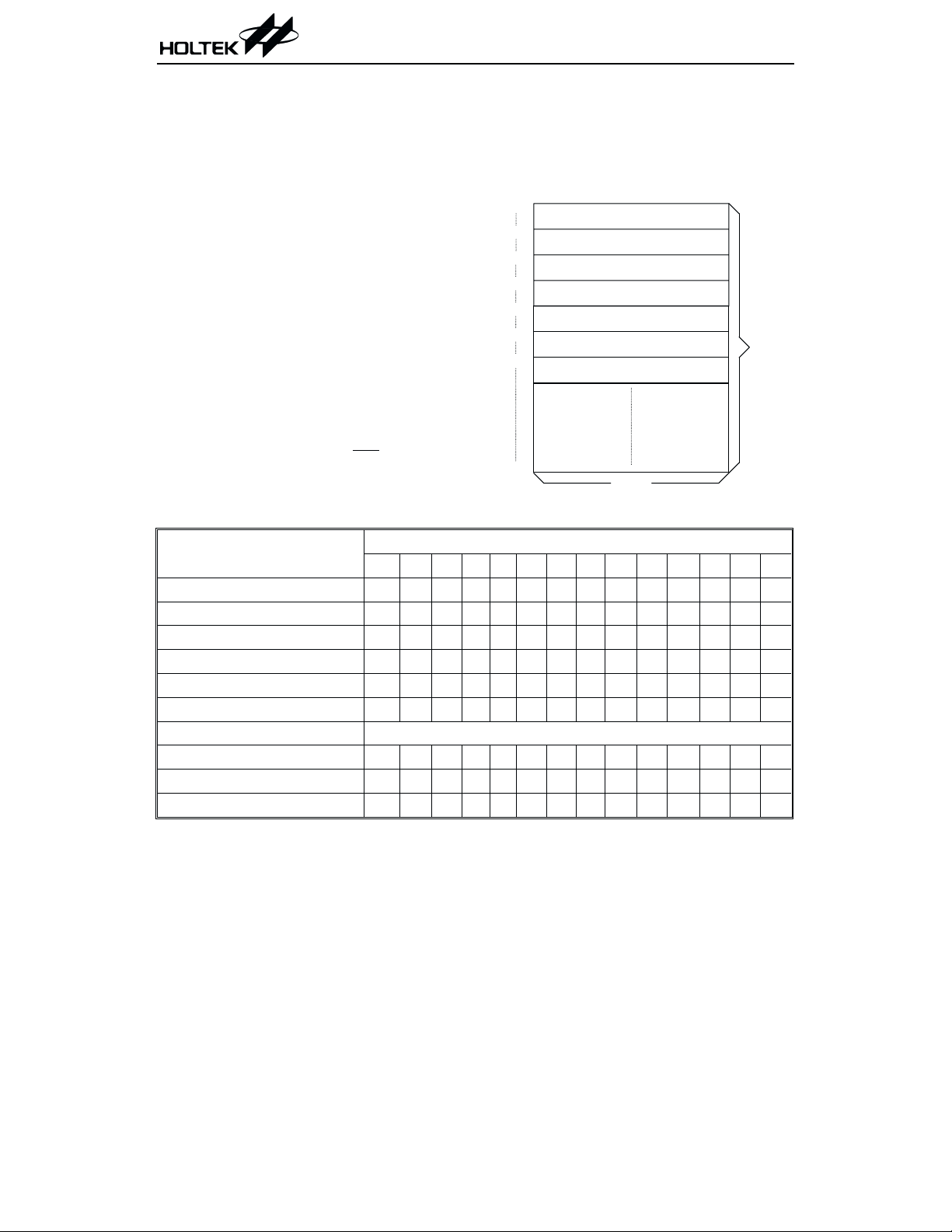
The state of the registers is summarized in the following table:
WDT
Register
TMR0H xxxx xxxx uuuu uuuu uuuu uuuu uuuu uuuu uuuu uuuu
TMR0L xxxx xxxx uuuu uuuu uuuu uuuu uuuu uuuu uuuu uuuu
TMR0C 00-0 1--- 00-0 1--- 00-0 1--- 00-0 1--- uu-u u---
TMR2 xxxx xxxx uuuu uuuu uuuu uuuu uuuu uuuu uuuu uuuu
TMR2C 00-0 1000 00-0 1000 00-0 1000 00-0 1000 uu-u uuuu
TMR3 xxxx xxxx uuuu uuuu uuuu uuuu uuuu uuuu uuuu uuuu
TMR3C 00-0 1000 00-0 1000 00-0 1000 00-0 1000 uu-u uuuu
INTCH 0000 0000 0000 0000 0000 0000 0000 0000 uuuu uuuu
TBHP xxxx xxxx uuuu uuuu uuuu uuuu uuuu uuuu uuuu uuuu
Program Counter 0000H 0000H 0000H 0000H 0000H
MP0 xxxx xxxx uuuu uuuu uuuu uuuu uuuu uuuu uuuu uuuu
MP1 xxxx xxxx uuuu uuuu uuuu uuuu uuuu uuuu uuuu uuuu
ACC xxxx xxxx uuuu uuuu uuuu uuuu uuuu uuuu uuuu uuuu
TBLP xxxx xxxx uuuu uuuu uuuu uuuu uuuu uuuu uuuu uuuu
TBLH xxxx xxxx uuuu uuuu uuuu uuuu uuuu uuuu uuuu uuuu
STATUS --00 xxxx --1u uuuu --uu uuuu --01 uuuu --11 uuuu
BP 0000 0000 0000 0000 0000 0000 0000 0000 uuuu uuuu
LCDC 0100 0000 0100 0000 0100 0000 0100 0000 uuuu uuuu
INTC 0000 0000 0000 0000 0000 0000 0000 0000 uuuu uuuu
WDTS 0000 0111 0000 0111 0000 0111 0000 0111 uuuu uuuu
PA 1111 1111 1111 1111 1111 1111 1111 1111 uuuu uuuu
PAC 1111 1111 1111 1111 1111 1111 1111 1111 uuuu uuuu
PB 1111 0000 1111 0000 1111 0000 1111 0000 uuuu uuuu
PBC 1111 0000 1111 0000 1111 0000 1111 0000 uuuu 0000
COMR 0000 0000 0000 0000 0000 0000 0000 0000 uuuu uuuu
PWMC 1111 1111 1111 1111 1111 1111 1111 1111 uuuu uuuu
PWM xxxx xxxx xxxx xxxx xxxx xxxx xxxx xxxx uuuu uuuu
X¢TALC
Reset
(Power On)
0000 0000 0000 0000 0000 0000 0000 0000 uuuu uuuu
Time-out
(Normal
Operation)
Reset
RES
(Normal
Operation)
RES
(HALT)
Reset
HTG2150
WDT
Time-out
(HALT)
*
Note:
²*² means ²warm reset²
²u² means ²unchanged²
²x² means ²unknown²
19 July 24, 2000

Preliminary
Label Bits Function
¾
TE 3
TON 4 To enable/disable timer counting (0=disabled; 1=enabled)
¾
TM0, TM1 6, 7 0, 1=Internal clock
0~2
Unused bits, read as ²0².
To define the TMR0 active edge of the timer counter
(0=active on low to high; 1=active on high to low)
5
Unused bits, read as ²x².
TMR0C register
HTG2150
When the timer counter (reading TMR0H) is
read, the clock will be blocked to avoid er
rors. As this may results in a counting error,
this must be taken into consideration by the
programmer.
Data Bus
R eload
O verflow
T o In te rr u p t
S ystem
C lock/4
Tim er C ounter 0
Preload R egister
Tim er
C ounter 0
Low Byte
Buffer
Timer counter 0
Timer 2/3
Timer 2 is an 8-bit counter, and its clock source
comes from the system clock divided by an
8-stage prescaler. There are two registers related to Timer 2 ; TMR2 (21H) and TMR2C
(22H). Two physical registers are mapped to
TMR2 location; writing TMR2 makes the start
ing value be placed in the Timer 2 preload regis
ter and reading the TMR2 gets the contents of
the Timer 2 counter. The TMR2C is a control
register, which defines the division ratio of the
prescaler and counting enable or disable.
Writing data to B2, B1 and B0 (bits 2, 1, 0 of
TMR2C) can yield various clock sources.
Once the Timer 2 starts counting, it will count
from the current contents in the counter to
FFH. Once an overflow occurs, the counter is
reloaded from a preload register, and generates
an interrupt request flag (T2F; bit 4 of INTCH).
To enable the counting operation, the timer On
bit (TON; bit 4 of TMR2C) should be set to ²1².
For proper operation, bit 6 of TMR2C should be
set to ²1² and bit 3, bit7 should be set to ²0².
The Timer 2 can also be used as PFD output by
setting PWM1 and PWM2 to be PFD and PFDB
output respectively by 2FH.7 and 2FH.6. When
the PFD/PFDB function is selected, setting
2FH.4/2FH.5 to ²1² will enable the PFD/PFDB
output and setting 2FH.4/2FH.5 to ²0² will dis
able the PFD/PFDB output. PFD Frequency:
T2f/[256-TMR2)´2]
Timer 3 has the same structure and operating
manner with Timer 2, except for clock source
and PFD function. The Timer 3 can be used as a
time base to generate a regular internal interrupt. The clock source of Timer 3 can come from
RTC OSC (X¢TAL 32kHz) or system clock divided by an 8-stage prescaler. If the RTC mask
option is enabled, a 32kHz crystal is needed
across XIN and XOUT pins. The 32kHz signal
is processed by an 8-stage prescaler to yield
various counting clock for Timer 3. There are 2
registers related to Timer 3; TMR3 (24H) and
TMR3C (25H). Writing data to B2, B1, B0 (bit 2,
1, 0 of TMR3C) can yield various counting clock.
-
20 July 24, 2000

SYS CLK
8-stage
Prescaler
Preliminary
D a ta B u s
Tim er 2
Preload R egister
R eload
HTG2150
TO N
T2f
Tim er 2
O verflow
To interrupt
2
¸
2FH .5
2FH .4
PW M 2
dac
PW M 1 dac
Timer 2
Label Bits Function
SSL 3~0 3~0 LCD common used
PFD 4 To enable/disable PFD output (0=disable; 1=enable)
PFDB 5 To enable/disable PFDB output (0=disable; 1=enable)
PWM1 6 To select PFDB/PWM1 output (0=PWM1; 1=PFDB)
PWM2 7 To select PFD/PWM2 output (0=PWM2; 1=PFD)
2FH register
near 32768H z
S ystem
Clock
32K X 'A TL
8 S tage P rescaler
m ask option
F0
2EH .7
F1
8 S tage P rescaler
Preload
T3f
Tim er 3
TO N
64
¸
LCD Driver
(512H z)
PW M 2
2FH .7
PW M 1
2FH .6
IN T
Timer 3
21 July 24, 2000

Preliminary
HTG2150
TMR2C
T2f
Bit 2 Bit 1 Bit 0
0 0 0 SYS CLK/2
0 0 1 SYS CLK/4
0 1 0 SYS CLK/8
0 1 1 SYS CLK/16
1 0 0 SYS CLK/32
1 0 1 SYS CLK/64
1 1 0 SYS CLK/128
1 1 1 SYS CLK/256
TMR2C bit 4 to enable/disable timer counting
(0=disable;1=enable)
TMR2C bit 3 always write ²0²
TMR2C bit 5 always write ²0²
TMR2C bit 6 always write ²1²
TMR2C bit 7 always write ²0²
F1 can select 4 frequency by mask option
Auto Mask Option F0
SYS CLK near 512kHz SYS CLK/16
SYS CLK near 1024kHz SYS CLK/32
SYS CLK near 2048kHz SYS CLK/64
SYS CLK near 4096kHz SYS CLK/128
TMR3C
T3f
Bit 2 Bit 1 Bit 0
0 0 0 F1/2
0 0 1 F1/4
0 1 0 F1/8
0 1 1 F1/16
1 0 0 F1/32
1 0 1 F1/64
1 1 0 F1/128
1 1 1 F1/256
Time base frequency= T3f / (256 - TMR3)
TMR3C bit 4 to enable/disable timer counting
(0=disable; 1=enable)
TMR3C bit 3 always write ²0²
TMR3C bit 5 always write ²0²
TMR3C bit 6 always write ²1²
TMR3C bit 7 always write ²0²
22 July 24, 2000

Preliminary
HTG2150
Input/output ports
There are 12 bidirectional input/output lines in
the HTG2150, labeled PA and PB, which are
mapped to the data memory of [12H], [14H], re
spectively. All these I/O ports can be used for in
put and output operations. For input operation,
these ports are non-latching, that is, the inputs
must be ready at the T2 rising edge of instruc
tion MOV A,[m] (m=12H, 14H). For output op
eration, all data is latched and remains
unchanged until the output latch is rewritten.
Each I/O line has its own control register (PAC,
PBC) to control the input/output configuration.
With this control register, CMOS output or
schmitt trigger input with or without pull-high
resistor (mask option) structures can be recon
figured dynamically under software control. To
function as an input, the corresponding latch of
the control register must write ²1². The
pull-high resistance will exhibit automatically
if the pull-high option is selected. The input
source also depends on the control register. If
the control register bit is ²1², the input will read
the pad state. If the control register bit is ²0²,
the contents of the latches will move to the in
ternal bus. The latter is possible in
²read-modify-write² instruction. For output
function, CMOS is the only configuration.
These control registers are mapped to locations
13H, 15H.
After a chip reset, these input/output lines stay
at high levels or floating (mask option). Each
bit of these input/output latches can be set or
cleared by the SET [m].i or CLR [m].i (m=12H,
14H) instruction.
Some instructions first input data and then fol
low the output operations. For example, the
SET [m].i, CLR [m].i, CPL [m] and CPLA [m]
instructions read the entire port states into the
CPU, execute the defined operations
(bit-operation), and then write the results back
to the latches or the accumulator.
Each line of port A has the capability to wake-up
the device. Port B are share pad, each pin func
tion are defined by mask option, the PB7 shares
with SEG36. The PB6, PB5 and PB4 share with
SEG35, SEG34 and SEG33. If the segment out
put is selected, the related I/O register (PB) can
not be used as general purpose register. Reading
the register will result to an unknown state.
PWM interface
The HTG2150 provides an 8 bit (bit 7 is a sign
bit) PWM D/A interface, which is good for
speech synthesis. The user can record or syn
thesize the sound and digitize it into the program ROM. These sound could be played back
in sequence of the functions as designed by the
internal program ROM. There are several algorithms that can be used in the HTG2150, they
are ... PCM, mLAW, DPCM, ADPCM..... .
-
-
-
-
-
DATA Bus
W rite C ontrol R egister
C hip R eset
R ead C ontrol R egister
W rite I/O
R ead I/O
System W ake-up (P A only)
Q
D
Q
CK
S
D
Q
CK
Q
S
M
U
X
M a s k O p tio n
Input/output ports
23 July 24, 2000
V
DD
WEAK
V
DD
Pull-up
M a s k O p tio n
PA0~PA7
PB4~PB7

Preliminary
HTG2150
The PWM circuit provides two pad outputs:
PWM2, PWM1 which can directly drive a piezo
ora32W speaker without adding any external
element. Refer to the Application Circuits.
The PWM clock source comes from the system
clock divided by a 3-bit prescaler. Setting data
to P0, P1 and P2 (bit 3, 4, 5 of 27H) can yield
various clock sources. The clock source are use
for PWM modulating clock and sampling clock.
After setting the start bit (bit 0 27H) and the
next falling edge coming from the prescaler, the
²DIV² will generate a serial clock to PWM coun
ter for modulating and PWMI for interrupt.
The PWM counter latch data at the first ²F1²
clock falling edge and the start counter at ²F1²
rising edge. The ²F2² clock is synchronous with
the first ²F1² clock and it is also connected to
the PWM output latch. In setting the ²start bit²
initial status, the ²PWM1 DAC² outputs a
²high² level and change the output status to
²LOW² while the ²7 bits counter² overflows.
BZ/SP
6/7
F1F2(Sampling
Bit
Rate
0 0 F0 F0/64
0 1 F0 F0/128
1 0 F0 F0/64
1 1 F0 F0/128
Device
32W speaker
32W speaker
Buzzer/8W
speaker
Buzzer/8W
speaker
On the above table, we can easily see that the
sampling rate is dependent on the system clock.
If start bit is set to ²0², the PWM2 and PWM1
will output a GND level voltage.
Label Bits Function
D/A 0 D/A control. 0:start ; 1:stop
BZ/SP 1
Bit 2
-
Output driver select
1:Buzzer ; 0:speaker
PWM counter bit select
1:7 bits ; 0:6 bits
3 bits preload counter,
P0~P2 3~5
bit 5/4/3:000B~111B (0~7)
bit 3:LSB
D0, D1 6, 7 PWMI
D0 D1 Samping Time/PWM Interrupt
00 1
01 2
10 4
11 8
PWM control register
bit0 bit1 bit2 bit3 bit4 bit5 bit6 bit7
7 bit D0 D1 D2 D3 D4 D5 D6 D7
6 bit X D1D2D3D4D5D6D7
Note: F1: for PWM modulation clock and F2
for sampling clock.
F0: system /[n+1] n=0~7
(n:3 bits preload counter)
F0
Start bit
Latch
F1
F2
7 bits PWM counter bit
Note:
X means don¢t care.
bit7: Sign bit
PWM data buffer
128 clock
O ne sam pling tim e
24 July 24, 2000

Data Bus
Preliminary
HTG2150
S ystem clock
Start bit
27H .0
PW M I
S ystem clock
Start bit
27H .0
PW M I
Prescaler
F0
Div.
F2
D a ta B u s
Prescaler
F0
Div.
F2
PW M Data
Buffer (28H)
F1
7 B its C ounter
CK
PE
PW M 1 dac
fo r 3 2
SPK
W
PW M 2 dac
fo r 3 2
SPK
W
27H.1=0 speaker
PW M Data
B u ffe r ( 2 8 H )
F1
7 B its C ounter
CK
PE
P W M 1 d a c fo r B Z
P W M 2 d a c fo r B Z
O verflow
O verflow
Sign bit
V
DD
DQ
QB
CK
R
V
DD
DQ
QB
CK
R
27H.1=1 buzzer
25 July 24, 2000

Preliminary
HTG2150
Mask option
The following shows many kinds of mask options in the HTG2150. All the mask options must be de
fined on order to ensure proper system functioning.
No. Mask Option
WDT enable/disable selection.
1
WDT can be enabled or disabled by mask option.
Wake-up selection. This option defines the wake-up activity. External I/O pins (PA only)
2
all have the capability to wake-up the chip from a HALT mode by a following edge.
External interrupt input pin share with other function selection.
3
/SEG37: INT can be set as an external interrupt input pin or LCD segment output
INT
pin.
I/O pins share with other function selection.
4
PB4/SEG33, PB5/SEG34, PB6/SEG35, PB7/SEG36: PB4, PB5, PB6, PB7 can be set as
I/O pins or LCD segment output pins.
Segment output pins share with other function selection.
5
XIN/SEG39, XOUT/SEG38: SEG38, SEG39 ban be set as LCD segment output pins or
XIN, XOUT pins be connected to a 32768Hz crystal.
LCD bias register selection. This option describes the LCD bias current. There are three
types of selection. *
6
· Selectable as small, middle or large current.
-
Note: *
S m a ll c u rre n t
V
DD
110k
W
110k
110k
110k
3/4 V
W
2/4 V
W
1/4 V
W
GND
M iddle current
V
DD
60k
W
DD
60k
DD
60k
DD
60k
3/4 V
2/4 V
1/4 V
GND
DD
DD
DD
W
W
W
Large current
V
DD
10k
W
3/4 V
10k
W
10k
10k
2/4 V
W
1/4 V
W
GND
DD
DD
DD
26 July 24, 2000

Application Circuits
Preliminary
HTG2150
32W speaker/B uzzer application
V
DD
*
32768H z
OSCI
RES
XIN/SEG 39
XOUT/SEG 38
INT/SEG 37
COM 0~CO M 7
SEG0~SEG39
(M a x .)
PA0~PA7
HTG 2150
PW M 1
PW M 2
1/4 B ias
LC D
PANEL
8W speaker application
32W SPK
or Buzzer
V
DD
*
32768H z
OSCI
RES
XIN/SEG 39
XOUT/SEG 38
INT/SEG 37
HTG 2150
COM 0~CO M 7
SEG0~SEG39
(M a x .)
PW M 2
PA0~PA7
1/4 B ias
LC D
PANEL
V
DD
8050
8
SPK
W
Note: * Optional capacitors can be added to get a more accurate frequency.
Since each crystal has its own chararacteristics, the user should consult the crystal manufacturer for appropriate value of the external capacitors.
27 July 24, 2000

Instruction Set Summary
Preliminary
HTG2150
Mnemonic Description
Arithmetic
ADD A,[m]
ADDM A,[m]
ADD A,x
ADC A,[m]
ADCM A,[m]
SUB A,x
SUB A,[m]
SUBM A,[m]
Add data memory to ACC
Add ACC to data memory
Add immediate data to ACC
Add data memory to ACC with carry
Add ACC to register with carry
Subtract immediate data from ACC
Subtract data memory from ACC
Subtract data memory from ACC with result in
data memory
SBC A,[m]
SBCM A,[m]
Subtract data memory from ACC with carry
Subtract data memory from ACC with carry with
result in data memory
DAA [m]
Decimal adjust ACC for addition with result in
data memory
Logic Operation
AND A,[m]
OR A,[m]
XOR A,[m]
ANDM A,[m]
ORM A,[m]
XORM A,[m]
AND A,x
OR A,x
XOR A,x
CPL [m]
CPLA [m]
AND data memory to ACC
OR data memory to ACC
Exclusive-OR data memory to ACC
AND ACC to data memory
OR ACC to data memory
Exclusive-OR ACC to data memory
AND immediate data to ACC
OR immediate data to ACC
Exclusive-OR immediate data to ACC
Complement data memory
Complement data memory with result in ACC
Increment and Decrement
INCA [m]
INC [m]
DECA [m]
DEC [m]
Increment data memory with result in ACC
Increment data memory
Decrement data memory with result in ACC
Decrement data memory
Instruction
Cycle
1
(1)
1
1
1
(1)
1
1
1
(1)
1
1
(1)
1
(1)
1
1
1
1
(1)
1
(1)
1
(1)
1
1
1
1
(1)
1
1
1
(1)
1
1
(1)
1
Flag
Affected
Z,C,AC,OV
Z,C,AC,OV
Z,C,AC,OV
Z,C,AC,OV
Z,C,AC,OV
Z,C,AC,OV
Z,C,AC,OV
Z,C,AC,OV
Z,C,AC,OV
Z,C,AC,OV
C
Z
Z
Z
Z
Z
Z
Z
Z
Z
Z
Z
Z
Z
Z
Z
28 July 24, 2000

Preliminary
HTG2150
Mnemonic Description
Rotate
RRA [m]
RR [m]
RRCA [m]
Rotate data memory right with result in ACC
Rotate data memory right
Rotate data memory right through carry with
result in ACC
RRC [m]
RLA [m]
RL [m]
RLCA [m]
Rotate data memory right through carry
Rotate data memory left with result in ACC
Rotate data memory left
Rotate data memory left through carry with
result in ACC
RLC [m]
Rotate data memory left through carry
Data Move
MOV A,[m]
MOV [m],A
MOV A,x
Move data memory to ACC
Move ACC to data memory
Move immediate data to ACC
Bit Operation
CLR [m].i
SET [m].i
Clear bit of data memory
Set bit of data memory
Branch
JMP addr
SZ [m]
SZA [m]
Jump unconditional
Skip if data memory is zero
Skip if data memory is zero with data movement
to ACC
SZ [m].i
SNZ [m].i
SIZ [m]
SDZ [m]
SIZA [m]
Skip if bit i of data memory is zero
Skip if bit i of data memory is not zero
Skip if increment data memory is zero
Skip if decrement data memory is zero
Skip if increment data memory is zero with
result in ACC
SDZA [m]
Skip if decrement data memory is zero with
result in ACC
CALL addr
RET
RET A,x
Subroutine call
Return from subroutine
Return from subroutine and load immediate data
to ACC
RETI
Return from interrupt
Table Read
TABRDC [m]
Read ROM code (current page) to data memory and
TBLH
TABRDL [m]
Read ROM code (last page) to data memory and
TBLH
Instruction
Cycle
1
(1)
1
1
(1)
1
1
(1)
1
1
(1)
1
1
(1)
1
1
(1)
1
(1)
1
2
(2)
1
(2)
1
(2)
1
(2)
1
(3)
1
(3)
1
(2)
1
(2)
1
2
2
2
2
(1)
2
(1)
2
Flag
Affected
None
None
C
C
None
None
C
C
None
None
None
None
None
None
None
None
None
None
None
None
None
None
None
None
None
None
None
None
29 July 24, 2000

Preliminary
HTG2150
Mnemonic Description
Miscellaneous
NOP
CLR [m]
SET [m]
CLR WDT
CLR WDT1
CLR WDT2
SWAP [m]
SWAPA [m]
HALT
No operation
Clear data memory
Set data memory
Clear Watchdog Timer
Pre-clear Watchdog Timer
Pre-clear Watchdog Timer
Swap nibbles of data memory
Swap nibbles of data memory with result in ACC
Enter power down mode
Note: x: 8 bits immediate data
m: 8 bits data memory address
A: accumulator
i: 0~7 number of bits
addr: 13 bits program memory address
Ö : Flag is affected
- : Flag is not affected
* : Flag may be affected by the execution status
(1)
: If a loading to the PCL register occurs, the execution cycle of instructions will be delayed
one for one more cycles (4 system clocks)
(2)
: If a skip to the next instruction occurs, the execution cycle of instructions will be delayed
one more cycle (4 system clocks). Otherwise the original instruction cycle(s) is unchanged.
(3):(1)or(2)
Instruction
Cycle
1
(1)
1
(1)
1
1
1
1
(1)
1
1
1
Flag
Affected
None
None
None
TO,PD
TO*,PD*
TO*,PD*
None
None
TO,PD
30 July 24, 2000

Preliminary
HTG2150
Instruction Definition
ADC A,[m] Add data memory and carry to accumulator
Description The contents of the specified data memory, accumulator and the carry flag
are added simultaneously, leaving the result in the accumulator.
Operation
Affected flag(s)
ADCM A,[m] Add accumulator and carry to data memory
Description The contents of the specified data memory, accumulator and the carry flag
Operation
Affected flag(s)
ADD A,[m] Add data memory to accumulator
Description The contents of the specified data memory and the accumulator are added.
Operation
Affected flag(s)
ACC ¬ ACC+[m]+C
TC2 TC1 TO PD OV Z AC C
¾¾¾¾ÖÖÖÖ
are added simultaneously, leaving the result in the specified data memory.
[m] ¬ ACC+[m]+C
TC2 TC1 TO PD OV Z AC C
¾¾¾¾ÖÖÖÖ
The result is stored in the accumulator.
ACC ¬ ACC+[m]
TC2 TC1 TO PD OV Z AC C
¾¾¾¾ÖÖÖÖ
ADD A,x Add immediate data to accumulator
Description The contents of the accumulator and the specified data are added, leaving
the result in the accumulator.
Operation
Affected flag(s)
ACC ¬ ACC+x
TC2 TC1 TO PD OV Z AC C
¾¾¾¾ÖÖÖÖ
31 July 24, 2000

Preliminary
ADDM A,[m] Add accumulator to data memory
Description The contents of the specified data memory and the accumulator are added.
The result is stored in the data memory.
Operation
Affected flag(s)
AND A,[m] Logical AND accumulator with data memory
Description Data in the accumulator and the specified data memory performs a bitwise
Operation
Affected flag(s)
AND A,x Logical AND immediate data to accumulator
Description Data in the accumulator and the specified data performs a bitwise logi
Operation
Affected flag(s)
[m] ¬ ACC+[m]
TC2 TC1 TO PD OV Z AC C
¾¾¾¾ÖÖÖÖ
logical_AND operation. The result is stored in the accumulator.
ACC ¬ ACC ²AND² [m]
TC2 TC1 TO PD OV Z AC C
¾¾¾¾¾Ö¾¾
cal_AND operation. The result is stored in the accumulator.
ACC ¬ ACC ²AND² x
TC2 TC1 TO PD OV Z AC C
¾¾¾¾¾Ö¾¾
HTG2150
-
ANDM A,[m] Logical AND data memory with accumulator
Description Data in the specified data memory and the accumulator performs a bitwise
logical_AND operation. The result is stored in the data memory.
Operation
Affected flag(s)
[m] ¬ ACC ²AND² [m]
TC2 TC1 TO PD OV Z AC C
¾¾¾¾¾Ö¾¾
32 July 24, 2000

Preliminary
CALL addr Subroutine call
Description The instruction unconditionally calls a subroutine located at the indicated
address. The program counter increments once to obtain the address of the
next instruction, and pushes this onto the stack. The indicated address is
then loaded. Program execution continues with the instruction at this ad
dress.
Operation
Affected flag(s)
CLR [m] Clear data memory
Description The contents of the specified data memory are cleared to zero.
Operation
Affected flag(s)
CLR [m].i Clear bit of data memory
Description The bit i of the specified data memory is cleared to zero.
Operation
Affected flag(s)
Stack ¬ PC+1
PC ¬ addr
TC2 TC1 TO PD OV Z AC C
¾¾¾¾¾¾¾¾
[m] ¬ 00H
TC2 TC1 TO PD OV Z AC C
¾¾¾¾¾¾¾¾
[m].i ¬ 0
TC2 TC1 TO PD OV Z AC C
¾¾¾¾¾¾¾¾
HTG2150
-
CLR WDT Clear Watchdog Timer
Description The WDT and the WDT Prescaler are cleared (re-counting from zero). The
power down bit (PD) and time-out bit (TO) are cleared.
Operation
Affected flag(s)
WDT and WDT Prescaler ¬ 00H
PD and TO ¬ 0
TC2 TC1 TO PD OV Z AC C
¾¾
00
33 July 24, 2000
¾¾¾¾

Preliminary
CLR WDT1 Preclear Watchdog Timer
Description The PD, TO flags, WDT and the WDT Prescaler are cleared (re-counting
from zero), if the other preclear WDT instruction had been executed. Execu
tion of this instruction without the other preclear instruction only sets the
indicating flag which implies that this instruction was executed and the PD
and TO flags remain unchanged.
Operation
Affected flag(s)
CLR WDT2 Preclear Watchdog Timer
Description The PD, TO flags, WDT and the WDT Prescaler are cleared (re-counting
Operation
Affected flag(s)
WDT and WDT Prescaler ¬ 00H*
PD and TO ¬ 0*
TC2 TC1 TO PD OV Z AC C
¾¾
from zero), if the other preclear WDT instruction had been executed. Execu
tion of this instruction without the other preclear instruction, only sets the
indicating flag which implies that this instruction was executed and the PD
and TO flags remain unchanged.
WDT and WDT Prescaler ¬ 00H*
PD and TO ¬ 0*
TC2 TC1 TO PD OV Z AC C
¾¾
0* 0*
0* 0*
¾¾¾¾
¾¾¾¾
HTG2150
-
-
CPL [m] Complement data memory
Description
Operation
Affected flag(s)
Each bit of the specified data memory is logically complemented (1¢s complement). Bits which previously contain a one are changed to zero and
vice-versa.
[m] ¬ [m
TC2 TC1 TO PD OV Z AC C
¾¾¾¾¾Ö¾¾
]
34 July 24, 2000

Preliminary
CPLA [m] Complement data memory and place result in accumulator
Description
Operation
Affected flag(s)
DAA [m] Decimal-Adjust accumulator for addition
Description The accumulator value is adjusted to the BCD (Binary Code Decimal) code.
Operation If (ACC.3~ACC.0) >9 or AC=1
Affected flag(s)
Each bit of the specified data memory is logically complemented (1¢s comple
ment). Bits which previously contained a one are changed to zero and
vice-versa. The complemented result is stored in the accumulator and the
contents of the data memory remains unchanged.
ACC ¬ [m
TC2 TC1 TO PD OV Z AC C
¾¾¾¾¾Ö¾¾
The accumulator is divided into two nibbles. Each nibble is adjusted to the
BCD code and an internal carry (AC1) will be done if the low nibble of the ac
cumulator is greater than 9. The BCD adjustment is done by adding 6 to the
original value if the original value is greater than 9 or a carry (AC or C) is set;
otherwise the original value remains unchanged. The result is stored in the
data memory and only the carry flag (C) may be affected.
then ([m].3~[m].0) ¬ (ACC.3~ACC.0)+6, AC1=AC
else ([m].3~[m].0) ¬ (ACC.3~ACC.0), AC1=0
and
If (ACC.7~ACC.4)+AC1 >9 or C=1
then ([m].7~[m].4) ¬ (ACC.7~ACC.4)+6+AC1, C=1
else ([m].7~[m].4) ¬ (ACC.7~ACC.4)+AC1, C=C
TC2 TC1 TO PD OV Z AC C
¾¾¾¾¾¾¾ Ö
]
HTG2150
-
-
DEC [m] Decrement data memory
Description Data in the specified data memory is decremented by one.
Operation
Affected flag(s)
[m] ¬ [m] -1
TC2 TC1 TO PD OV Z AC C
¾¾¾¾¾Ö¾¾
35 July 24, 2000

Preliminary
DECA [m] Decrement data memory and place result in accumulator
Description Data in the specified data memory is decremented by one, leaving the result
in the accumulator. The contents of the data memory remain unchanged.
Operation
Affected flag(s)
HALT Enter power down mode
Description This instruction stops the program execution and turns off the system clock.
Operation
Affected flag(s)
ACC ¬ [m]-1
TC2 TC1 TO PD OV Z AC C
¾¾¾¾¾Ö¾¾
The contents of the RAM and registers are retained. The WDT and prescaler
are cleared. The power down bit (PD) is set and the WDT time-out bit (TO) is
cleared.
PC ¬ PC+1
PD ¬ 1
TO ¬ 0
TC2 TC1 TO PD OV Z AC C
¾¾
01
¾¾¾¾
HTG2150
INC [m] Increment data memory
Description Data in the specified data memory is incremented by one.
Operation
Affected flag(s)
INCA [m] Increment data memory and place result in accumulator
Description Data in the specified data memory is incremented by one, leaving the result
Operation
Affected flag(s)
[m] ¬ [m]+1
TC2 TC1 TO PD OV Z AC C
¾¾¾¾¾Ö¾¾
in the accumulator. The contents of the data memory remain unchanged.
ACC ¬ [m]+1
TC2 TC1 TO PD OV Z AC C
¾¾¾¾¾Ö¾¾
36 July 24, 2000

Preliminary
JMP addr Direct Jump
Description Bits 0~12 of the program counter are replaced with the directly-specified ad
dress unconditionally, and control is passed to this destination.
Operation
Affected flag(s)
MOV A,[m] Move data memory to accumulator
Description The contents of the specified data memory is copied to the accumulator.
Operation
Affected flag(s)
MOV A,x Move immediate data to accumulator
Description The 8-bit data specified by the code is loaded into the accumulator.
Operation
Affected flag(s)
PC ¬ addr
TC2 TC1 TO PD OV Z AC C
¾¾¾¾¾¾¾¾
ACC ¬ [m]
TC2 TC1 TO PD OV Z AC C
¾¾¾¾¾¾¾¾
ACC ¬ x
TC2 TC1 TO PD OV Z AC C
¾¾¾¾¾¾¾¾
HTG2150
-
MOV [m],A Move accumulator to data memory
Description The contents of the accumulator is copied to the specified data memory (one
of the data memory).
Operation
Affected flag(s)
[m] ¬ ACC
TC2 TC1 TO PD OV Z AC C
¾¾¾¾¾¾¾¾
37 July 24, 2000

Preliminary
NOP No operation
Description No operation is performed. Execution continues with the next instruction.
Operation
Affected flag(s)
OR A,[m] Logical OR accumulator with data memory
Description Data in the accumulator and the specified data memory (one of the data
Operation
Affected flag(s)
OR A,x Logical OR immediate data to accumulator
Description Data in the accumulator and the specified data performs a bitwise logi
Operation
Affected flag(s)
PC ¬ PC+1
TC2 TC1 TO PD OV Z AC C
¾¾¾¾¾¾¾¾
memories) performs a bitwise logical_OR operation. The result is stored in
the accumulator.
ACC ¬ ACC ²OR² [m]
TC2 TC1 TO PD OV Z AC C
¾¾¾¾¾Ö¾¾
cal_OR operation. The result is stored in the accumulator.
ACC ¬ ACC ²OR² x
TC2 TC1 TO PD OV Z AC C
¾¾¾¾¾Ö¾¾
HTG2150
-
ORM A,[m] Logical OR data memory with accumulator
Description Data in the data memory (one of the data memories) and the accumulator
performs a bitwise logical_OR operation. The result is stored in the data
memory.
Operation
Affected flag(s)
[m] ¬ ACC ²OR² [m]
TC2 TC1 TO PD OV Z AC C
¾¾¾¾¾Ö¾¾
38 July 24, 2000

Preliminary
RET Return from subroutine
Description Theprogramcounterisrestoredfromthestack.Thisisatwo-cycleinstruction.
Operation
Affected flag(s)
RET A,x Return and place immediate data in accumulator
Description The program counter is restored from the stack and the accumulator loaded
Operation
Affected flag(s)
RETI Return from interrupt
Description The program counter is restored from the stack, and interrupts are enabled
Operation
Affected flag(s)
PC ¬ Stack
TC2 TC1 TO PD OV Z AC C
¾¾¾¾¾¾¾¾
with the specified 8-bit immediate data.
PC ¬ Stack
ACC ¬ x
TC2 TC1 TO PD OV Z AC C
¾¾¾¾¾¾¾¾
by setting the EMI bit. EMI is the enable master (global) interrupt bit (bit 0;
register INTC).
PC ¬ Stack
EMI ¬ 1
TC2 TC1 TO PD OV Z AC C
¾¾¾¾¾¾¾¾
HTG2150
RL [m] Rotate data memory left
Description The contents of the specified data memory is rotated one bit left, with bit 7
rotated into bit 0.
Operation
Affected flag(s)
[m].(i+1) ¬ [m].i; [m].i:bit i of the data memory (i=0-6)
[m].0 ¬ [m].7
TC2 TC1 TO PD OV Z AC C
¾¾¾¾¾¾¾¾
39 July 24, 2000

Preliminary
RLA [m] Rotate data memory left and place result in accumulator
Description Data in the specified data memory is rotated one bit left, with bit 7 rotated
into bit 0, leaving the rotated result in the accumulator. The contents of the
data memory remain unchanged.
Operation
Affected flag(s)
RLC [m] Rotate data memory left through carry
Description The contents of the specified data memory and the carry flag are together ro
Operation
Affected flag(s)
ACC.(i+1) ¬ [m].i; [m].i:bit i of the data memory (i=0-6)
ACC.0 ¬ [m].7
TC2 TC1 TO PD OV Z AC C
¾¾¾¾¾¾¾¾
tated one bit left. Bit 7 replaces the carry bit; the original carry flag is ro
tated into the bit 0 position.
[m].(i+1) ¬ [m].i; [m].i:bit i of the data memory (i=0-6)
[m].0 ¬ C
C ¬ [m].7
TC2 TC1 TO PD OV Z AC C
¾¾¾¾¾¾¾ Ö
HTG2150
-
-
RLCA [m] Rotate left through carry and place result in accumulator
Description Data in the specified data memory and the carry flag are together rotated
one bit left. Bit 7 replaces the carry bit and the original carry flag is rotated
into bit 0 position. The rotated result is stored in the accumulator but the
contents of the data memory remain unchanged.
Operation
Affected flag(s)
ACC.(i+1) ¬ [m].i; [m].i:bit i of the data memory (i=0-6)
ACC.0 ¬ C
C ¬ [m].7
TC2 TC1 TO PD OV Z AC C
¾¾¾¾¾¾¾ Ö
40 July 24, 2000

Preliminary
RR [m] Rotate data memory right
Description The contents of the specified data memory are rotated one bit right with bit 0
rotated to bit 7.
Operation
Affected flag(s)
RRA [m] Rotate right and place result in accumulator
Description Data in the specified data memory is rotated one bit right with bit 0 rotated
Operation
Affected flag(s)
RRC [m] Rotate data memory right through carry
Description The contents of the specified data memory and the carry flag are together ro
Operation
Affected flag(s)
[m].i ¬ [m].(i+1); [m].i:bit i of the data memory (i=0-6)
[m].7 ¬ [m].0
TC2 TC1 TO PD OV Z AC C
¾¾¾¾¾¾¾¾
into bit 7, leaving the rotated result in the accumulator. The contents of the
data memory remain unchanged.
ACC.(i) ¬ [m].(i+1); [m].i:bit i of the data memory (i=0-6)
ACC.7 ¬ [m].0
TC2 TC1 TO PD OV Z AC C
¾¾¾¾¾¾¾¾
tated one bit right. Bit 0 replaces the carry bit; the original carry flag is rotated into the bit 7 position.
[m].i ¬ [m].(i+1); [m].i:bit i of the data memory (i=0-6)
[m].7 ¬ C
C ¬ [m].0
TC2 TC1 TO PD OV Z AC C
¾¾¾¾¾¾¾ Ö
HTG2150
-
41 July 24, 2000

Preliminary
RRCA [m] Rotate right through carry and place result in accumulator
Description Data of the specified data memory and the carry flag are together rotated
one bit right. Bit 0 replaces the carry bit and the original carry flag is rotated
into the bit 7 position. The rotated result is stored in the accumulator. The
contents of the data memory remain unchanged.
Operation
Affected flag(s)
SBC A,[m] Subtract data memory and carry from accumulator
Description The contents of the specified data memory and the complement of the carry
Operation
Affected flag(s)
ACC.i ¬ [m].(i+1); [m].i:bit i of the data memory (i=0-6)
ACC.7 ¬ C
C ¬ [m].0
TC2 TC1 TO PD OV Z AC C
¾¾¾¾¾¾¾ Ö
flag are together subtracted from the accumulator, leaving the result in the
accumulator.
ACC ¬ ACC+[m
TC2 TC1 TO PD OV Z AC C
¾¾¾¾ÖÖÖÖ
]+C
HTG2150
SBCM A,[m] Subtract data memory and carry from accumulator
Description The contents of the specified data memory and the complement of the carry
flag are together subtracted from the accumulator, leaving the result in the
data memory.
Operation
Affected flag(s)
[m] ¬ ACC+[m
TC2 TC1 TO PD OV Z AC C
¾¾¾¾ÖÖÖÖ
]+C
42 July 24, 2000

Preliminary
SDZ [m] Skip if decrement data memory is zero
Description The contents of the specified data memory are decremented by one. If the re
sult is zero, the next instruction is skipped. If the result is zero, the following
instruction, fetched during the current instruction execution, is discarded
and a dummy cycle is replaced to get the proper instruction. This makes a
two-cycle instruction. Otherwise proceed with the next instruction.
Operation
Affected flag(s)
SDZA [m] Decrement data memory and place result in ACC, skip if zero
Description The contents of the specified data memory are decremented by one. If the re
Operation
Affected flag(s)
Skip if ([m]-1)=0, [m] ¬ ([m]-1)
TC2 TC1 TO PD OV Z AC C
¾¾¾¾¾¾¾¾
sult is zero, the next instruction is skipped. The result is stored in the accu
mulator but the data memory remains unchanged. If the result is zero, the
following instruction, fetched during the current instruction execution, is
discarded and a dummy cycle is replaced to get the proper instruction, that
makes a two-cycle instruction. Otherwise proceed with the next instruction.
Skip if ([m]-1)=0, ACC ¬ ([m]-1)
TC2 TC1 TO PD OV Z AC C
¾¾¾¾¾¾¾¾
HTG2150
-
-
-
SET [m] Set data memory
Description Each bit of the specified data memory is set to one.
Operation
Affected flag(s)
[m] ¬ FFH
TC2 TC1 TO PD OV Z AC C
¾¾¾¾¾¾¾¾
43 July 24, 2000

Preliminary
SET [m].i Set bit of data memory
Description Bit i of the specified data memory is set to one.
Operation
Affected flag(s)
SIZ [m] Skip if increment data memory is zero
Description The contents of the specified data memory is incremented by one. If the re
Operation
Affected flag(s)
SIZA [m] Increment data memory and place result in ACC, skip if zero
Description The contents of the specified data memory is incremented by one. If the re
Operation
Affected flag(s)
[m].i ¬ 1
TC2 TC1 TO PD OV Z AC C
¾¾¾¾¾¾¾¾
sult is zero, the following instruction, fetched during the current instruction
execution, is discarded and a dummy cycle is replaced to get the proper in
struction. This is a two-cycle instruction. Otherwise proceed with the next
instruction.
Skip if ([m]+1)=0, [m] ¬ ([m]+1)
TC2 TC1 TO PD OV Z AC C
¾¾¾¾¾¾¾¾
sult is zero, the next instruction is skipped and the result is stored in the ac
cumulator. The data memory remains unchanged. If the result is zero, the
following instruction, fetched during the current instruction execution, is
discarded and a dummy cycle is replaced to get the proper instruction. This
is a two-cycle instruction. Otherwise proceed with the next instruction.
Skip if ([m]+1)=0, ACC ¬ ([m]+1)
TC2 TC1 TO PD OV Z AC C
¾¾¾¾¾¾¾¾
HTG2150
-
-
-
-
44 July 24, 2000

Preliminary
SNZ [m].i Skip if bit i of the data memory is not zero
Description If bit i of the specified data memory is not zero, the next instruction is
skipped. If bit i of the data memory is not zero, the following instruction,
fetched during the current instruction execution, is discarded and a dummy
cycle is replaced to get the proper instruction. This is a two-cycle instruction.
Otherwise proceed with the next instruction.
Operation
Affected flag(s)
SUB A,[m] Subtract data memory from accumulator
Description The specified data memory is subtracted from the contents of the accumula
Operation
Affected flag(s)
SUBM A,[m] Subtract data memory from accumulator
Description The specified data memory is subtracted from the contents of the accumula
Operation
Affected flag(s)
Skip if [m].i¹0
TC2 TC1 TO PD OV Z AC C
¾¾¾¾¾¾¾¾
tor, leaving the result in the accumulator.
ACC ¬ ACC+[m
TC2 TC1 TO PD OV Z AC C
¾¾¾¾ÖÖÖÖ
tor, leaving the result in the data memory.
[m] ¬ ACC [m
TC2 TC1 TO PD OV Z AC C
¾¾¾¾ÖÖÖÖ
]+1
]+1
HTG2150
-
-
SUB A,x Subtract immediate data from accumulator
Description The immediate data specified by the code is subtracted from the contents of
the accumulator, leaving the result in the accumulator.
Operation
Affected flag(s)
ACC ¬ ACC+x
TC2 TC1 TO PD OV Z AC C
¾¾¾¾ÖÖÖÖ
+1
45 July 24, 2000

Preliminary
SWAP [m] Swap nibbles within the data memory
Description The low-order and high-order nibbles of the specified data memory (one of
the data memories) are interchanged.
Operation
Affected flag(s)
SWAPA [m] Swap data memory and place result in accumulator
Description The low-order and high-order nibbles of the specified data memory are inter
Operation
Affected flag(s)
SZ [m] Skip if data memory is zero
Description If the contents of the specified data memory is zero, the following instruc
Operation Skip if [m]=0
Affected flag(s)
[m].3~[m].0 « [m].7~[m].4
TC2 TC1 TO PD OV Z AC C
¾¾¾¾¾¾¾¾
changed, writing the result to the accumulator. The contents of the data
memory remain unchanged.
ACC.3~ACC.0 ¬ [m].7~[m].4
ACC.7~ACC.4 ¬ [m].3~[m].0
TC2 TC1 TO PD OV Z AC C
¾¾¾¾¾¾¾¾
tion, fetched during the current instruction execution, is discarded and a
dummy cycle is replaced to get the proper instruction. This is a two-cycle instruction. Otherwise proceed with the next instruction.
TC2 TC1 TO PD OV Z AC C
¾¾¾¾¾¾¾¾
HTG2150
-
-
46 July 24, 2000

Preliminary
SZA [m] Move data memory to ACC, skip if zero
Description The contents of the specified data memory is copied to the accumulator. If the
contents is zero, the following instruction, fetched during the current in
struction execution, is discarded and a dummy cycle is replaced to get the
proper instruction. This is a two-cycle instruction. Otherwise proceed with
the next instruction.
Operation Skip if [m]=0
Affected flag(s)
TC2 TC1 TO PD OV Z AC C
¾¾¾¾¾¾¾¾
SZ [m].i Skip if bit i of the data memory is zero
Description If bit i of the specified data memory is zero, the following instruction, fetched
during the current instruction execution, is discarded and a dummy cycle is
replaced to get the proper instruction. This is a two-cycle instruction. Other
wise proceed with the next instruction.
Operation Skip if [m].i=0
Affected flag(s)
TC2 TC1 TO PD OV Z AC C
¾¾¾¾¾¾¾¾
HTG2150
-
-
TABRDC [m] Move ROM code (current page) to TBLH and data memory
Description The ROM code low byte (current page) addressed by the table pointer
(TBLP), (TBHP) is moved to the specified data memory and the high byte
transferred to TBLH directly.
Operation
Affected flag(s)
[m] ¬ ROM code (low byte)
TBLH ¬ ROM code (high byte)
TC2 TC1 TO PD OV Z AC C
¾¾¾¾¾¾¾¾
47 July 24, 2000

Preliminary
TABRDL [m] Move the ROM code (last page) to TBLH and data memory
Description The ROM code low byte (last page) addressed by the table pointer (TBLP) is
moved to the data memory and the high byte transferred to TBLH directly.
Operation
Affected flag(s)
XOR A,[m] Logical XOR accumulator with data memory
Description Data in the accumulator and the indicated data memory performs a bitwise
Operation
Affected flag(s)
XORM A,[m] Logical XOR data memory with accumulator
Description Data in the indicated data memory and the accumulator perform a bitwise
Operation
Affected flag(s)
[m] ¬ ROM code (low byte)
TBLH ¬ ROM code (high byte)
TC2 TC1 TO PD OV Z AC C
¾¾¾¾¾¾¾¾
logical Exclusive_OR operation and the result is stored in the accumulator.
ACC ¬ ACC ²XOR² [m]
TC2 TC1 TO PD OV Z AC C
¾¾¾¾¾Ö¾¾
logical Exclusive_OR operation. The result is stored in the data memory. The
zero flag is affected.
[m] ¬ ACC ²XOR² [m]
TC2 TC1 TO PD OV Z AC C
¾¾¾¾¾Ö¾¾
HTG2150
XOR A,x Logical XOR immediate data to accumulator
Description Data in the the accumulator and the specified data perform a bitwise logical
Exclusive_OR operation. The result is stored in the accumulator. The zero
flag is affected.
Operation
Affected flag(s)
ACC ¬ ACC ²XOR² x
TC2 TC1 TO PD OV Z AC C
¾¾¾¾¾Ö¾¾
48 July 24, 2000

Preliminary
HTG2150
Holtek Semiconductor Inc. (Headquarters)
No.3 Creation Rd. II, Science-based Industrial Park, Hsinchu, Taiwan, R.O.C.
Tel: 886-3-563-1999
Fax: 886-3-563-1189
Holtek Semiconductor Inc. (Taipei Office)
5F, No.576, Sec.7 Chung Hsiao E. Rd., Taipei, Taiwan, R.O.C.
Tel: 886-2-2782-9635
Fax: 886-2-2782-9636
Fax: 886-2-2782-7128 (International sales hotline)
Holtek Semiconductor (Hong Kong) Ltd.
RM.711, Tower 2, Cheung Sha Wan Plaza, 833 Cheung Sha Wan Rd., Kowloon, Hong Kong
Tel: 852-2-745-8288
Fax: 852-2-742-8657
Copyright Ó 2000 by HOLTEK SEMICONDUCTOR INC.
The information appearing in this Data Sheet is believed to be accurate at the time of publication. However, Holtek
assumes no responsibility arising from the use of the specifications described. The applicationsmentioned herein are
used solely for the purpose of illustration and Holtek makes no warranty or representation that such applications
will be suitable without further modification, nor recommends the use of its products for application that may pres
ent a risk to human life due to malfunction or otherwise. Holtek reserves the right to alter its products without prior
notification. For the most up-to-date information, please visit our web site at http://www.holtek.com.tw.
49 July 24, 2000
-
 Loading...