

Page 1

Features
•
Operating voltage: 2.4V~3.3V
•
Eight input lines
•
Two output lines
•
Five working registers
•
RC oscillator for system clock
•
Crystal oscillator for RTC and LCD clock
•
8K×8 program ROM
•
156×4 data RAM
•
50×8 segment LCD driver, 1/5 bias, 1/8 duty
•
8-bit programmable timer with built-in
frequency source
General Description
The HTG12G0 is a 4-bit singl e chip microcontroller specially designed for LCD product applications.
HTG12G0
Microcontroller
•
Internal timer overflow and RTC interrupt
•
16 kinds of programmable sound effects
•
Halt function and wake-up feature
reduce power consumption
•
One-level subroutine nesting
•
8-bit table read instruction
•
Up to 4.0µs instruction cycle with 1.0MHz
system clock at V
•
95 powerful instructions
It is ideally suited for applications requiring
low power consumption, with many L CD segments such as calculator , scale, subsystem controller, hand-held LCD products and electroni c
appliances.
DD
=3V
1 14th May ’99
Page 2
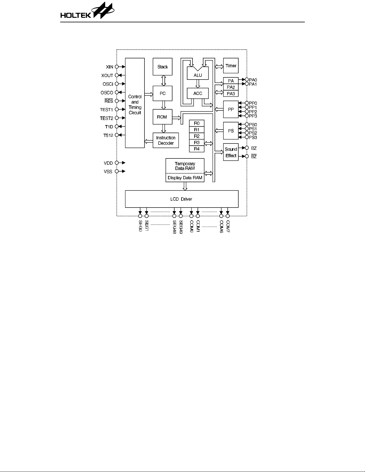
Block Diagram
HTG12G0
Notes: ACC: Accumulator PC: Program counter
R0~R4: Working registers P A0~PA1: Output ports
PP , PS: Input ports PA3: ROM bank control bit
PA2: LCD on/off switch
2 14th May ’99
Page 3
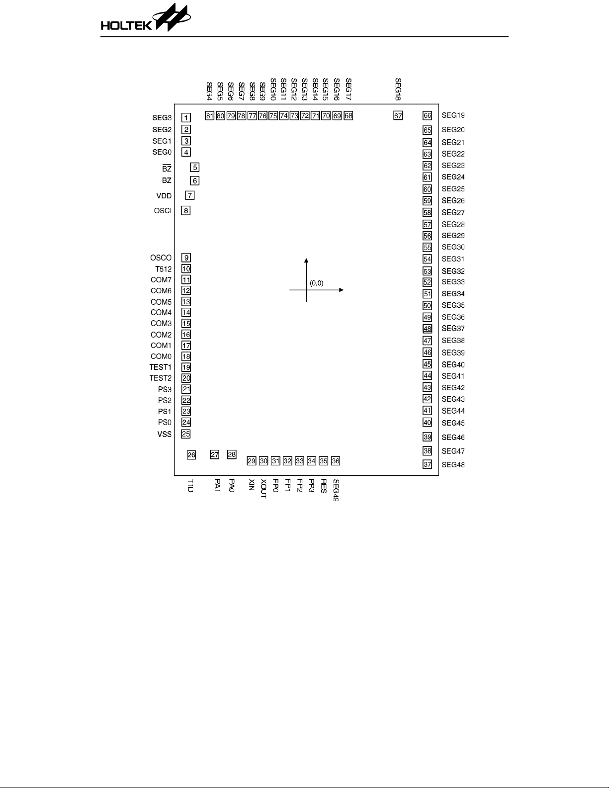
Pad Assignment
HTG12G0
Chip size: 3070 × 4440 (µm)
* The IC substrate should be connected to VSS in the PCB layout artwork.
3 14th May ’99
2
Page 4
HTG12G0
Pad Coordinates Unit: µm
Pad No. X Y Pad No. X Y
1 –1403.50 2012.75 42 1412.00 –1270.25
2 –1403.50 1872.75 43 1412.00 –1134.25
3 –1403.50 1741.75 44 1412.00 –998.25
4 –1403.50 1610.75 45 1412.00 –862.25
5 –1304.00 1431.75 46 1412.00 –726.25
6 –1304.00 1276.25 47 1412.00 –590.25
7 –1358.50 1104.25 48 1412.00 –454.25
8 –1409.50 929.25 49 1412.00 –318.25
9 –1403.50 377.75 50 1412.00 –182.25
10 –1403.50 249.75 51 1412.00 –46.25
11 –1403.50 121.75 52 1412.00 89.75
12 –1403.50 –6.25 53 1412.00 225.75
13 –1403.50 –134.25 54 1412.00 361.75
14 –1403.50 –262.25 55 1412.00 497.75
15 –1403.50 –390.25 56 1412.00 633.75
16 –1403.50 –518.25 57 1412.00 769.75
17 –1403.50 –646.25 58 1412.00 905.75
18 –1403.50 –774.25 59 1412.00 1041.75
19 –1403.50 –902.25 60 1412.00 1177.75
20 –1403.50 –1030.25 61 1412.00 1313.75
21 –1403.50 –1158.25 62 1412.00 1449.75
22 –1403.50 –1286.25 63 1412.00 1585.25
23 –1403.50 –1414.25 64 1412.00 1720.75
24 –1403.50 –1542.25 65 1412.00 1865.25
25 –1409.50 –1680.75 66 1412.00 2034.75
26 –1342.00 –1926.25 67 1071.50 2037.25
27 –1071.50 –1920.25 68 490.00 2034.75
28 –871.50 –1920.25 69 358.00 2034.75
29 –640.00 –1994.75 70 228.00 2034.75
30 –500.00 –1994.75 71 105.00 2034.75
31 –360.00 –1994.75 72 –18.00 2034.75
32 –220.00 –1994.75 73 –141.00 2034.75
33 –80.00 –1994.75 74 –264.00 2034.75
34 60.00 –1994.75 75 –387.00 2034.75
35 200.00 –1994.75 76 –510.00 2034.75
36 340.00 –1994.75 77 –633.00 2034.75
37 1412.00 –2034.75 78 –756.00 2034.75
38 1412.00 –1877.25 79 –879.00 2034.75
39 1412.00 –1712.25 80 –1002.00 2034.75
40 1412.00 –1542.25 81 –1129.50 2034.75
41 1412.00 –1406.25
4 14th May ’99
Page 5
Pad Description
Pad No. Pad name I/O Mask Option Description
1~4,
36~81
5
6
7 VDD I — Positive power supply
8
9
10
19
20
26
11~18 COM7~COM0 O — Output for LCD panel common plate
21~24 PS3~PS0 I
25 VSS I — Negative power supply, GND
27
28
29
30
31~34 PP0~PP3 I
35
SEG3~SEG0
SEG49~SEG4
BZ
BZ
OSCI
OSCO
T512
TEST1
TEST2
T1D
PA1
PA0
XIN
XOUT
RES I —
O — LCD driver outputs for LCD panel segment
O * Sound effect output
I
O
O
I
I
O
O
I
O
—
—
Pull-high or
None
**
CMOS or
NMOS
Open Drain
— 32768Hz crystal oscillator for time base
Pull-high or
None
**
An external resistor between OSCI and OSCO
is needed for internal system clock.
For test mode only
TEST1 and TEST2 must be open when the
HTG12G0 is in normal operation (with an
internal pull high resistor)
4-bit port for input only
2-bit latch port for output only
4-bit port for input only
Input for reset LSI inside
Reset is active at logical low level
HTG12G0
*: 6 internal sources deriving from the system clock can be selected as sound effect clock by mask
option. If Holtek’s sound library is invoked, only 128K and 64K is accepted.
**: Each bit of input ports PS, PP can be a trigger source of HALT interrupt. That can be specified
by mask option.
Absolu te Maximu m R a tin g s
Supply Voltage .........................VSS–0.3V to 13V Operating Temperature...................0°C to 70°C
Input V oltage.......................V
Note: These are stress ratings only. Stresses exceeding the range spe cified under “Absolute Maxi-
mum Ratings” may cause substantial damage to the device. Functional operation of this device
at other conditions beyond those listed in the specification is not implied and prolonged
exposure to extreme condition s may affect device reliability.
–0.3 to VDD+0.3 Storage Temperature.................–50°C to 125°C
SS
5 14th May ’99
Page 6
HTG12G0
D.C. Characteristics Ta=25°C
Symbol Parameter
V
DD
I
DD
Operating Voltage — — 2.4 — 3.3 V
Operating Current 3V No load, f
Standby Current
I
STB
(RTC OSC ON)
and LCD ON
V
V
V
V
I
I
I
I
I
I
I
I
R
R
IL1
IH1
IL2
IH2
OL1
OH1
OL2
OH2
OL3
OH3
OL4
OH4
PH1
PH2
Input Low Voltage 3V PS, PP 0 — 0.6 V
Input High Voltage 3V PS, PP 2.1 — 3.0 V
Input Low Voltage 3V RES 0 — 0.6 V
Input High Voltage 3V RES 2.5 — 3.0 V
Port A, BZ and BZ
Output Sink Current
Port A, BZ and BZ
Output Source Current
Segment 0~7 Output
Sink Current
Segment 0~7 Output
Source Current
Segment 8~49 Output
Sink Current
Segment 8~49 Output
Source Current
Common Output Sink
Current
Common Output
Source Current
Pull-high Resistance 3V PS, PP 15 — 200 kΩ
Pull-high Resistance 3V RES 100 — 300 kΩ
Test Conditions
V
DD
Conditions
=500kHz — 100 500 µA
SYS
Min. Typ. Max. Uint
3V System halt — 10 20
3V V
3V V
3V V
3V V
3V V
3V V
3V V
3V V
=3V, VOL=0.3V 1.5 3.0 — mA
DD
=3V, VOH=2.7V –0.5 –1.5 — mA
DD
=3V, VOL=0.3V 80 100 — µA
LCD
=3V, VOH=2.7V –50 –70 — µA
LCD
=3V, VOL=0.3V 40 60 — µA
LCD
=3V, VOH=2.7V –20 –40 — µA
LCD
=3V, VOL=0.3V 100 120 — µA
LCD
=3V, VOH=2.7V –100 –130 — µA
LCD
µA
6 14th May ’99
Page 7
HTG12G0
A.C. Characteristics Ta=25°C
Symbol Parameter
f
SYS
f
LCD
t
COM
t
CY
t
RES
f
SOUND
System Clock 3V R:620kΩ~51kΩ 100 — 1000 kHz
LCD Clock 3V — — 512 — Hz
LCD Common Period — 1/8 duty — (1/f
Cycle Time — f
Reset Pulse Width — — 5 — — ms
Sound Effect Clock — — — 64 or 128* — kHz
Test Conditions
V
DD
Conditions
=1.0MHz — 4.0 — µs
SYS
Min. Typ. Max. Unit
)x8 — sec
LCD
*: Only these two clock signal frequencies are supported by Holtek sound library.
7 14th May ’99
Page 8
Functional Description
Program counter – PC
The 12-bit program counter is controlled by PA3
which can change the ROM bank of the program
memory. There are two program memory banks
which are selected by PA3, e ach bank is 4KB
ROM. The instruction“OUT PA, A” is used to
change the value of PA3. Then, low or hi gh 4K
ROM is selected accordingly. All instructions
are not effective on the crossin g bank, unless
the value of PA3 is changed in advance.
The 12-bit program counter (PC) controls the
sequence in which the instructions stored in the
program ROM are executed and its contents
specify a max. of 4096 address.
After accessing a memory word to fetch an instruction code, the contents of the program
counter are incremented by one or two, then the
program counter will point to the memory word
containing the next instruction code.
Mode
Initial
reset
Internal
interrupt
External
interrupt
Jump, call
instruction
Conditional
branch
Return from
subroutine
PA3 PC11 PC10 PC9 PC8 PC7 PC6 PC5 PC4 PC3 PC2 PC1 PC0
1 0 00000000 000
PA30 00000000 1 00
PA30 00000001 0 00
PA3 PC11 PC10 PC9 PC8 PC7 PC6 PC5 PC4 PC3 PC2 PC1 PC0
PA3 @ PC10 PC9 PC8 PC7 PC6 PC5 PC4 PC3 PC2 PC1 PC0
PA3 S11 S10 S9 S8 S7 S6 S5 S4 S3 S2 S1 S0
HTG12G0
When executing the jump instruction (JMP,
JNZ, JC, JTMR...), subro uti ne cal l, intern al interrupt, RTC inte rrupt or return from su broutine, the PC manipulate s the pro gram transfer
by loading the address corresponding to each
instruction.
Progr a m me mory – ROM
The program memory is used to store program
instruction which is to be execu ted . It is orga nized into 8192
gram counter and PA3.
Certain locations in bank 0 of the program
memory are reserved for specific usage:
•
Location 0004H
This area is reserved for TIMER interrupt
service program. A timer interrupt results
from TIMER overflow, if interrupt is enabled,
the CPU begins execution at location 0004H.
Program Counter
×8 bits and addressed by the pro-
Notes: PC11~PC0: Instruction code bits @: PC11 keeps current value
S11~S0: Stack register bits P A3: Bank value bits
8 14th May ’99
Page 9
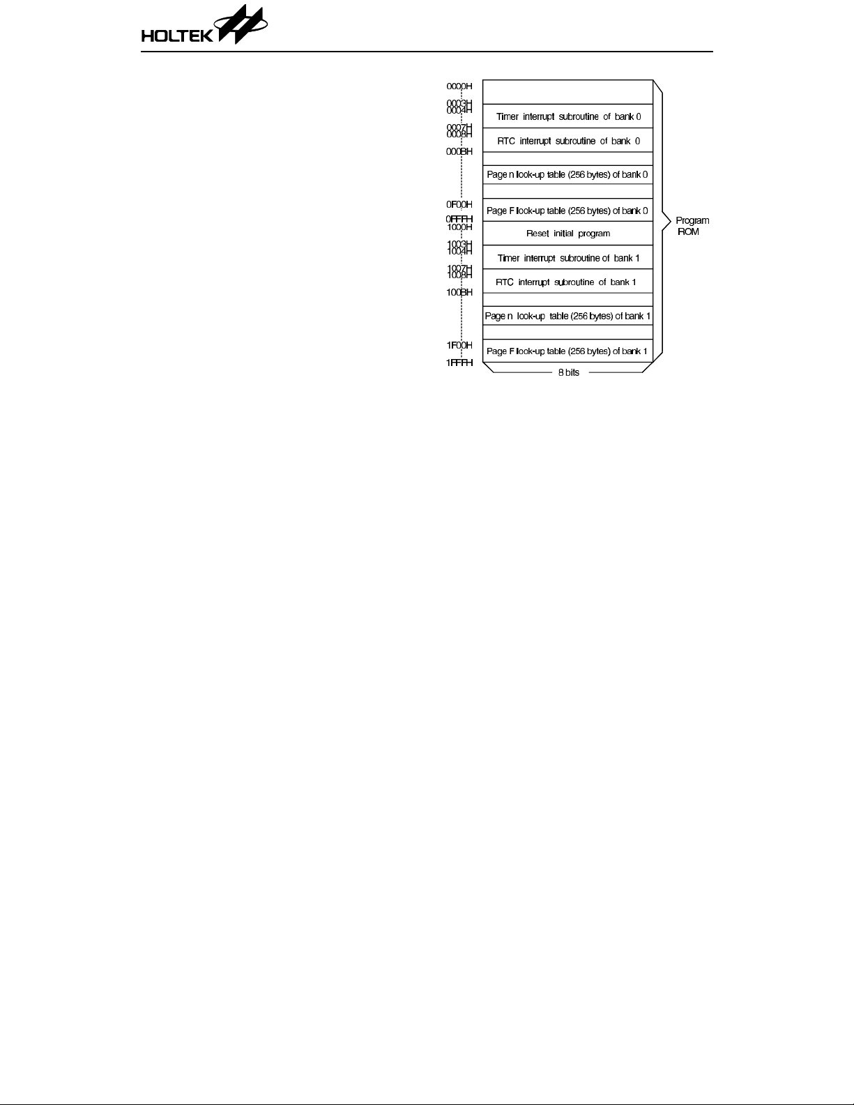
•
Location 0008H
This area is reserved for RTC interrup t serv-
ice program.
•
Location 0n00H~0nFF H (n=current number)
and 0F00H~0FFFH.
The last 256 bytes of each page in the program
memory, addressed f rom 0n00H to 0n FFH and
0F00H to 0FFFH can be used as a look–up
table. The instructions READ R4A, READ
MR0A, READF R4A, READF MR0A can read
the table and transfer the contents of the table
to ACC and R4 or transfer to ACC and data
memory addresse d by register p air “R1, R0”.
These areas may function as a normal program memory depending on the requirements.
Certain locations in bank 1 of the program
memory are reserved for specific usage:
•
Location 1000H
This area is reserved for the initialization pro-
gram. After reset, the CPU always begins execution at location 1000H.
•
Location 1004H
This area is reserved for TIMER interrupt
service program. A timer interrupt results
from TIMER overflow, if interrupt is enabled,
the CPU begins execution at location 1004H.
•
Location 1008H
This area is reserved for RTC interrup t serv-
ice program.
•
Location 1n00H~1nFF H (n=current number)
and 1F00H~1FFFH.
The last 256 bytes of each page in the program
memory, addressed f rom 1n00H to 1n FFH and
1F00H to 1FFFH can be used as a look–up
table. The instructions READ R4A, READ
MR0A, READF R4A, READF MR0A can read
the table and transfer the contents of the table
to ACC and R4 or transfer to ACC and data
memory addresse d by register p air “R1, R0”.
These areas may function as a normal program memory depending on the requirements.
The program memory (ROM) mapping is
shown below:
HTG12G0
Program memory
In the execution of an instruction, the program counter is added before the executing
phase. So a careful manipulation of READ
MR0A and READ R4A is needed in the page
margin.
Stack register
This is a special group of register which is used
to save the contents of the program counter
(PC) and is organized with 13 bits
bit is used to sto re the ca rry flag. An inte rrupt
will force the contents of the PC and the carry
flag onto the stack register. A subroutine call
will also cause the PC contents to be pushed
onto the stack; however the carry flag will not
be stored. At the en d of a subroutine or interrupt routine which is signaled by a return instruction, RET or RETI restores the program
counter to its previous value from stack register.
Executing “RETI” instruction will restore the
carry flag from the stack register, but “RET”
does not.
×1 level. One
9 14th May ’99
Page 10
HTG12G0
Working registers – R0, R1, R2, R3, R4
These five registers are usually used to store the
frequently accessed data. Th e workin g regi ster
can be incremented (+1) or decremented (–1).
The JNZ Rn,address (n=0,1,4) instruction
makes very efficient use of the working register
as program loop counter. The register pairs of
R1, R0 and R3, R2 can also be used as the data
memory pointer, when the data memory transfer instruction is executed.
Data memory – RAM
The data memory is a static RAM organized
with 256
× 4 bits and is used to store temporary
data and display data. All of the data memory
locations are indirectly addressable through the
register pair “R1, R0” or “R3, R2”.
There are two areas in the data memory , temporary data area and display data area. Access to
temporary data memory is made through
00H~9BH address, an d access to display data
memory is made in 9CH~FFH address.
When data is written in the di splay area, the
LCD driver automatically reads it and generates an LCD driving signal.
Data memory
Accumulator – ACC
The register ACC plays the most important role
in data manipulation and data transfer. It is not
only one of the s ources of inp ut to the A LU bu t
also the destin ation of the result due to ALU.
Data transfer can be performed b etween ACC
and other registers, data memory or I/O ports.
Arithmetic and log ic unit – ALU
This circuit performs arithmeti c and logic operation. The AL U provides the fol lowing functions:
•
Arithmetic operation
(ADD, ADC, SUB, SBC, DAA)
•
Logic operation (AND, OR, XOR)
•
Rotation (RL, RR, RLC, RRC)
•
Increment and Decrement (INC, DEC)
•
Branch decision (JZ, JNZ, JC, JNC...)
The ALU not only outputs the results of data
operation but also sets the status of carry flag
(C) in some instructions.
Timer
This is a programmable 8–bit count-up counter ,
internal frequency sources used to aid the user
in counting and generating accurate time base.
The Timer can be pre-set and read with software instructions. “TIMER XXH”, “MOV
TMRL, A” and “MOV TMRH, A” preload TIMER
value. “MOV A, TMR L” and “MOV A, TMRH”
read the contents of TIMER to ACC.
The Timer is stopped by a hardware reset or
“TIMER OFF” instruction and started by a
TIMER ON instruction.
Once the Timer is started, it will in crement to
its maximum count (FFH) and overflows to zero
(00H). It will not stop until there is a “TIMER
OFF” instruction or reset. When an overflow
occurs, it will set the Timer Flag (T F) simultaneously. If interrupt is enabled, the Timer circuit supports TF for internal interrupt. The
state of the TF can be tested with the conditional instruction JTMR.
The Timer flag is cleared after the interrupt or
JTMR instruction is executed.
The frequency of the internal frequency so urce
can be selected by mask option.
Frequency of TIMER clock
system clock
=
n
2
Where n=0,1,2......13 except 6, by mask option
(the sixth stage is reserved for internal use).
10 14th May ’99
Page 11

HTG12G0
RTC
There is a real time clock (RTC) function implemented on the HTG12G0. The RT C function is
used to generate an accurate time period . The
clock source of the RT C circuit come s from the
32768Hz crystal oscillator. The block diagram is
shown as follows:
The output of the RTC can be selected by mask
option.
Frequency of the RTC output =
256
n
2
n=0~7
The RTC output is u sed to generate an interrupt signal.
Interrupt
The HTG12G0 provides both TIMER and RTC
interrupt modes. The DI and EI instructions are
used to disable and enable the interrupts. When
the RTC is activated during enable interrupt
mode and the program is not within a CALL
subroutine, this causes a subroutine call to location 8 and reset the interrupt latch.
Likewise when the timer flag is set in the enable
interrupt mode and the program is not within a
CALL subroutine, the TIMER interrupt is activated. This cause a subroutine call to location 4
and resets the tim er flag. If both TIMER and
RTC interrupts arrive at the same time, the
RTC will be serviced first.
When running under a CALL subroutine or DI
the interrupt ackn owledge is on hold until the
RET or EI instruction is invoked. The CALL
instruction should not be used withi n an interrupt routine as unpredictable behaviors may
occur . If within a CALL subroutine both TIMER
and RTC interrupt occur, no matter what order
they arrive in, the RTC interrupt wil l be serviced first after leaving the CALL subroutine.
This also app lies if the two inte rrupts arrive at
the same time.
The interrupts are disabled by a hardware reset
or a DI instruction. They remai n disab led until
the EI instruction is executed.
Initial reset
The HTG12G0 provides a RES pin for system
initialization. Since the
pull high resistor, only an external 0.1
RES pin has internal
µ~1µ ca-
pacitor is needed. If the reset pulse is generated externally , it must be held low for at least
5 ms.
When
RES is active, the internal block wi ll be
initialized as shown below:
PA3 and PC 1000H
TIMER Stop
Timer flag Reset (low)
SOUND Sound off and one sing mode
Output port A High (or floating state)
LCD output Disabled
BZ and
output
HALT
BZ
High level
This is a special feature of HTG12G0. It will
stop the chip’s normal operation and reduces
power consumption. When the instruction
“HALT” is executed, then
•
System oscillator will be stopped
•
The contents of the on-chip RAM and
registers remain unchanged
•
RTC oscillator still keeps running
The system can escape HALT mode by ways of
initial reset or RTC interrup t or wake-up from
the followi ng ent ry of pr ogra m count er valu e.
•
Initial reset: 1000H
Wake-up: next addres s of the HALT instruc-
tion
When the halt status is terminated by the
RTC interrupt, the following proce dure takes
place:
Case1: If the system is in an interrupt-dis-
*
able state before entering the halt state:
11 14th May ’99
Page 12

–
The system will be awakened and returns
to the main program instruction following
the HALT command.
–
The RTC inte rrupt will be held unti l the
system receives a n enable interrupt command by which the RTC inte rrupt will be
serviced.
Case 2: If the system is in an interrupt
*
enable state:
–
The RTC interrupt will awake the system
and execute the RTC interrupt subroutine.
–
In the HALT mod e, each bit of ports PP,
PS, can be used as wake-up signal by mask
option to wake-up the system. This signal
is active in low-going transition.
Sound effect
HTG12G0 provides sound effect circuit which
offers up to 16 sounds with 3 effects of tone,
boom and noise. Holtek supports a sound library which have melody, alarm, machine gun
shooting etc.
Whenever the instruction “SOUND n” or
“SOUND A” is executed, the specified sound
begins playing. Whenever “SOUND OFF” is
executed, it terminates the singing sound immediately.
There are two singing modes, SONE mode and
SLOOP mode, which is acti vated by “SOUND
ONE” and “SOUND LOOP”. In SONE mode,
the sound that has been specified plays just
once. In SLOOP mode, the sound being specified
keeps playing repeatedly.
Since sound 0~11 contain 32 notes, sound 12~15
contain 64 notes, the later possess better sound
than the former.
The frequency of the sound effect circuit can be
selected by mask option.
Frequency
of sound effect circuit =
system
2
clock
m
Where m=0, 1, 2, 3, 4, 5
Holtek’s sound library only supports sound
clock frequency 128K or 64K. To utilize Holtek’s
sound library, select the proper system clock
and mask option.
HTG12G0
LCD display memory
The LCD display memory is embedded in the
data memory. It can be read and written to as
normal data memory.
The figure shows the mapping between display
memory and LCD pattern.
To turn o n/off the d ispl ay, the programmer just
writes 1/0 to the corresponding bit of the display
memory .
The LCD display module may have any form a s
long as the number of the common is no more
than 8 and the segment is n o more than 50.
LCD display memory
LCD driver output
The output number of the LCD driver is 50 × 8,
directly driving a 1/8 duty cycle and 1/5 bias
LCD. All LCD segments are at random during
initial clear mode.
The LCD has built-in bias voltage circuit. No
external resistor is needed.
The frequency of the LCD driving clock is fixed
at about 512Hz. This is set by RTC OSC
(32.768kHz).
12 14th May ’99
Page 13

HTG12G0
LCD driver output can be en abled or disabl ed
by setting PA2 without the influence o f the related memory condition.
LCD driver output is enabled by setting PA2 as
“1”, and disabled by setting PA2 as “0”.
An example of an LCD driving waveform (1/8
duty and 1/5 bias) is shown below:
Oscillator circuit
Only one external resistor is required for the
HTG12G0 system clock.
The system clock is also used as the sound effect
clock, or internal frequency so urce of TIMER.
Another crystal oscillator is needed to be used
as the reference signal of LCD driving clock and
RTC interrupt clock source.
The HTG12G0 ma chine cycle consists of a sequence of 4 states numbered T1 to T4. Each
state lasts for one oscillator period. The machine cycle is 4.0
up to 1.0MHz.
µs, if the system freque ncy is
Input ports – PS, PP
Ports PS, PP are 4-bit input ports. These input
ports are configured as shown below:
All of these p orts h ave inte rna l p ull -high res is tor determined by mask option.
Each bit of input ports PS, PP can be a tri gger
source of HALT interrupt. That is also specified
by mask optio n. A transition from high to low
will make HTG12G0 wake-up.
Input ports PS, PP
RC and RTC oscillator
13 14th May ’99
Page 14
HTG12G0
Output port – PA
Port A is a 2-bit output port (PA0~PA1), and
configured as shown below:
Output port PA
The mask option available for selecting the output configuration is ei ther normal CMOS output type or open drain NMOS output type. At
the initial clear mode , the output ports are at
high state (in CMOS output type) or at floating
state (in NMOS output type).
Note:
PA3 controls the bit 12 of the progra m counte r.
When th e instru ction “OUT PA, A” is operated,
port A is changed as well. PA2 controls the
ON/OFF state of the LCD . Without the influence of the memory condition, “1” turns the LCD
on, and “0” off.
Mask option
HTG12G0 provides six kinds of mask option for
different applications.
•
Each bit of input ports P S, PP with pu ll-high
resistor
•
Each bit of input ports PS, PP function as
HALT wake-up trigger
•
Each bit of output port PA0~PA1 with CMOS
or open drain NMOS
•
8 bit programmable TIMER with internal frequency sources. There a re 13 (the s ixth sta ge
is reserved for internal use) internal frequency sources which can be selected as a
clocking signal.
•
Six kinds of sound clock frequencies:
f
/2m, m= 0, 1, 2, 3, 4, 5
SYS
•
There are eight kinds of RTC interrupt frequencies. RTC interrupt frequency= 256/2
n
Hz, n=0~7
14 14th May ’99
Page 15

Application Circuits
HTG12G0
R*: depends on the required system clock frequency (R=51kΩ~620kΩ, at VDD=3V)
15 14th May ’99
Page 16

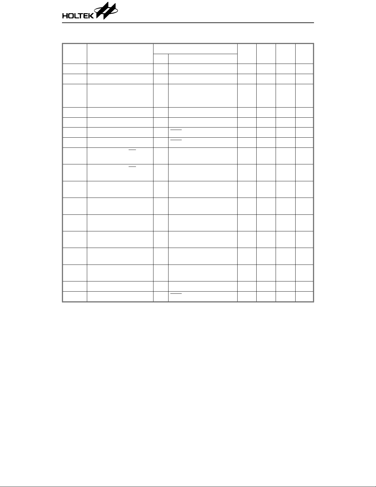
Instruction Set Summary
Mnemonic Description Byte Cycle CF
Arithmetic
ADD A,[R1R0]
ADC A,[R1R0]
SUB A,[R1R0]
SBC A,[R1R0]
ADD A,XH
SUB A,XH
DAA
Logic Operation
AND A,[R1R0]
OR A,[R1R0]
XOR A,[R1R0]
AND [R1R0],A
OR [R1R0],A
XOR [R1R0],A
AND A,XH
OR A,XH
XOR A,XH
Increment and
Decrement
INC A
INC Rn
INC [R1R0 ]
INC [R3R2 ]
DEC A
DEC Rn
DEC [R1R0]
DEC [R3R2]
Data Move
MOV A,Rn
MOV Rn,A
MOV A,[R1R0]
MOV A,[R3R2]
MOV [R1R0],A
MOV [R3R2],A
MOV A,XH
MOV R1R0,XXH
MOV R3R2,XXH
MOV R4,XH
Add data memory to ACC
Add data memory with carry to ACC
Subtract data memory from ACC
Subtract data memory from ACC with borrow
Add immediate data to ACC
Subtract immediate data from ACC
Decimal adjust ACC for addition
AND data memory to ACC
OR data memory to ACC
Exclusive-OR data memory to ACC
AND ACC to data memory
OR ACC to data memory
Exclusive–OR ACC to data memory
AND immediate data to ACC
OR immediate data to ACC
Exclusive–OR immediate data to ACC
Increment ACC
Increment register
Increment data memory
Increment data memory
Decrement ACC
Decrement register
Decrement data memory
Decrement data memory
Move register to ACC
Move ACC to register
Move data memory to ACC
Move data memory to ACC
Move ACC to data memory
Move ACC to data memory
Move immediate data to ACC
Move immediate data to R1 and R0
Move immediate data to R3 and R2
Move immediate data to R4
1
1
1
1
2
2
1
1
1
1
1
1
1
2
2
2
1
1
1
1
1
1
1
1
1
1
1
1
1
1
1
2
2
2
HTG12G0
1
√
1
√
1
√
1
√
2
√
2
√
1
√
—
1
—
1
—
1
—
1
—
1
—
1
—
2
—
2
—
2
—
1
—
1
—
1
—
1
—
1
—
1
—
1
—
1
—
1
—
1
—
1
—
1
—
1
—
1
—
1
—
2
—
2
—
2
16 14th May ’99
Page 17
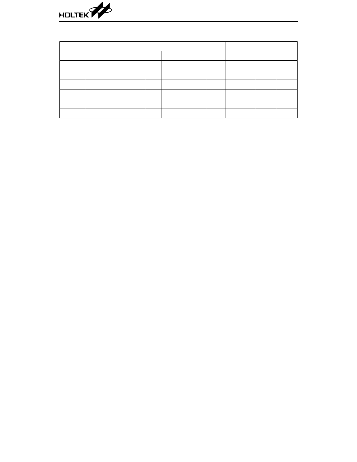
HTG12G0
Mnemonic Description Byte Cycle CF
Rotate
RL A
RLC A
RR A
RRC A
Input & Output
IN A,Pi
OUT PA,A
Branch
JMP addr
JC addr
JNC addr
JTMR addr
JAn addr
JZ A,addr
JNZ A,addr
JNZ Rn,addr
Subroutine
CALL addr
RET
RETI
Flag
CLC
STC
EI
DI
NOP
Timer
TIMER XXH
TIMER ON
TIMER OFF
MOV A,TMRL
MOV A,TMRH
MOV TMRL,A
MOV TMRH,A
Table Read
READ R4A
READ MR0A
READF R4A
READF MR0A
Rotate ACC left
Rotate ACC left through the carry
Rotate ACC right
Rotate ACC right through the carry
Input port–i to ACC, port–i=PS, PP
Output ACC to port-A
Jump unconditional
Jump on carry=1
Jump on carry=0
Jump on timer out
Jump on ACC bit n=1, n=0,1,2,3
Jump on ACC is zero
Jump on ACC is n ot zero
Jump on register Rn not zero, n=0,1,4
Subroutine call
Return from subroutine or interrupt
Return from interrupt service routine
Clear carry flag
Set carry flag
Enable interrupt
Disable interrupt
No operation
Set 8 bits immediate data to TIMER
Set TIMER to start counting
Set TIMER to stop counting
Move low nibble o f TIMER to ACC
Move high nibble of TIMER to ACC
Move ACC to low nibble of TIMER
Move ACC to high nibble of TIMER
Read ROM code of current page to R4 & ACC
Read ROM code of current page to M(R1,R0), ACC
Read ROM code of page F to R4 & ACC
Read ROM code of page F to M(R1,R0), ACC
1
1
1
1
1
1
2
2
2
2
2
2
2
2
2
1
1
1
1
1
1
1
2
1
1
1
1
1
1
1
1
1
1
1
√
1
√
1
√
1
√
1
—
1
—
—
2
—
2
—
2
—
2
—
2
—
2
—
2
—
2
2
—
1
—
1
√
0
1
1
1
—
1
—
1
—
1
—
2
—
1
—
1
—
1
—
1
—
1
—
1
—
2
—
2
—
2
—
2
17 14th May ’99
Page 18

HTG12G0
Mnemonic Description Byte Cycle CF
Sound Control
—
2
SOUND n
SOUND A
SOUND ONE
SOUND LOOP
SOUND OFF
Miscellaneous
HALT Enter power down mode 2 2 —
Active SOUND channel n
Active SOUND channel with Accumulator
Turn on SOUND one mode
Turn on SOUND repeat mode
Turn off SOUND
2
—
1
1
—
1
1
—
1
1
—
1
1
18 14th May ’99
Page 19

HTG12G0
Instruction Definitions
ADC A,[R1R0] Add data memory contents and carry to accumulator
Machine code 0 0 0 0 1 0 0 0
Description The contents of the data memory addressed by the register pair “R1,R0” and
the carry are added to the accumulato r. Carry is affected.
Operation ACC
ADD A,XH Add immediate data to accumulator
Machine code 0 1 0 0 0 0 0 0 0 0 0 0 d d d d
Description The specified data is added to the accumulator. Carry is affected.
Operation ACC
ADD A,[R1R0] Add data memory contents to accumulator
Machine code 0 0 0 0 1 0 0 1
Description The contents of the data memo ry addressed b y the register pai r “R1,R0” is
Operation ACC
AND A,XH Logical AND immediate data to accumulator
Machine code 0 1 0 0 0 0 1 0 0 0 0 0 d d d d
Description Data in the accumulator is logical AND with the immediate data specified by
Operation ACC
← ACC+M(R1,R0)+CF
← ACC+XH
added to the accumulator. Carry is affected.
← ACC+M(R1,R0)
the code.
← ACC “AND” XH
AND A,[R1R0] Logical AND accumulator with data memory
Machine code 0 0 0 1 1 0 1 0
Description Data in the accumulator is logical AND with the data memory addressed by
the register pair “R1,R0”.
Operation ACC
AND [R1R0],A Logical AND data memory with accumulator
Machine code 0 0 0 1 1 1 0 1
Description Data in the data memory a ddressed by the register p air “R1,R0” is logical
Operation M(R1,R0)
← ACC “AND” M(R1,R0)
AND with the accumulator
← M(R1,R0) “AND” ACC
19 14th May ’99
Page 20

HTG12G0
CALL address Subroutine call
Machine code 1 1 1 1 a a a a a a a a a a a a
Description The program counter bits 0~11 are saved in the stack and the specified
address loaded into the program counter.
Operation Stack
CLC Clear carry flag
Machine code 0 0 1 0 1 0 1 0
Description The carry flag is reset to 0
Operation CF
DAA Decimal-Adjust accumulator
Machine code 0 0 1 1 0 1 1 0
Description The accumulator val ue is adjusted to BCD (Binary Code Decima l), if the
Operation If ACC>9 or CF=1 then
DEC A Decrement accumulator
Machine code 0 0 1 1 1 1 1 1
Description Data in the accumulator is decremented by 1. Carry flag is not affected.
Operation ACC
← PC+2
PC
← address
← 0
contents of the accumulato r is greater than 9 or CF (Carry flag) is 1.
ACC
← ACC+6, CF ← 1
else
ACC
← ACC, CF ← CF
← ACC–1
DEC Rn Decrement register
Machine code 0 0 0 1 n n n 1
Description Data in the working register “Rn” is decremented by 1. Carry flag is not
affected.
Operation Rn
DEC [R1R0] Decrement data memory
← Rn–1; Rn=R0,R1,R2,R3,R4, for nnn=0,1,2,3,4
Machine code 0 0 0 0 1 1 0 1
Description Data in the data memory spe cified by the register pair “R1,R0” is decre-
mented by 1. Carry flag is not affected.
Operation M(R1,R0)
← M(R1,R0)–1
20 14th May ’99
Page 21

HTG12G0
DEC [R3R2] Decrement data memory
Machine code 0 0 0 0 1 1 1 1
Description Data in the data memory spe cified by the register pair “R3,R2” is decre-
mented by 1. Carry flag is not affected.
Operation M(R3,R2)
DI Disable interrupt
Machine code 0 0 1 0 1 1 0 1
Description Internal time-out interrupt and external interrupt are disabled.
EI Enable interrupt
Machine code 0 0 1 0 1 1 0 0
Description Internal time-out interrupt and external interrupt are enabled.
HALT Halt system clock
Machine code 0 0 1 1 0 1 1 1 0 0 1 1 1 1 1 0
Description Turn off system clock, and enter power down mode.
Operation PC
IN A,Pi Input port to accumulator
Machine code 0 0 1 1 0 0 1 1 PS
0 0 1 1 0 1 0 0 PP
Description The data on p ort “Pi” is transferred to the accumulator.
Operation ACC
← M(R3,R2)–1
← PC+2
← Pi; Pi=PS or PP
INC A Increment accumulator
Machine code 0 0 1 1 0 0 0 1
Description Data in the accumulator is incremented by 1. Carry flag is not affected.
Operation ACC
INC Rn Increment register
← ACC+1
Machine code 0 0 0 1 n n n 0
Description Data in the working regi ster “Rn” is incremented by 1. Carry flag is not
affected.
Operation Rn
INC [R1R0] Increment data memory
← Rn+1; Rn=R0~R4 for nnn=0~4
Machine code 0 0 0 0 1 1 0 0
Description Data in the data memory specified by the register pair “R1,R0” is incre-
mented by 1. Carry flag is not affected.
Operation M(R1,R0)
← M(R1,R0)+1
21 14th May ’99
Page 22

HTG12G0
INC [R3R2] Increment data memory
Machine code 0 0 0 0 1 1 1 0
Description Data memory s pecified by the register pair “R3,R2” i s incremented by 1.
Carry flag is not affected.
Operation M(R3,R2)
JAn address Jump if accumulator bit n is set
Machine code 1 0 0 n n a a a a a a a a a a a
Description Bits 0~10 of the progra m counter are replaced with the directly-speci fied
address but bit 11 of the program counter is unaffected, if accumulator bit n
is set to 1.
Operation PC (bit 0~10)
PC
JC address Jump if carry is set
Machine code 1 1 0 0 0 a a a a a a a a a a a
Description Bits 0~10 of the progra m counter are replaced with the directly-speci fied
address but bit 11 of the program counter is unaffected, if the CF (Carry flag)
is set to 1.
Operation PC (bit 0~10)
PC
← M(R3,R2)+1
← address, if ACC bit n=1(n=0~3)
← PC+2, if ACC bit n=0
← address, if CF=1
← PC+2, if CF=0
JMP address Direct jump
Machine code 1 1 1 0 a a a a a a a a a a a a
Description Bits 0~11 of the program counter are replaced with the directly-specified
address.
Operation PC
JNC address Jump if carry is not set
← address
Machine code 1 1 0 0 1 a a a a a a a a a a a
Description Bits 0~10 of the progra m counter are replaced with the directly-speci fied
address and bit 11 of the program counter is unaffected, if the CF (Carry flag)
is set to 0.
Operation PC (bit 0~10)
PC
← PC+2, if CF=1
JNZ A,address Jump if accumulator is not 0
← address, if CF=0
Machine code 1 0 1 1 1 a a a a a a a a a a a
Description Bits 0~10 of the progra m counter are replaced with the directly-speci fied
address but bit 11 of the program counter is unaffected, if the accumulator is
not 0.
Operation PC (bit 0~10)
PC
← PC+2, if ACC=0
← address, if A CC≠ 0
22 14th May ’99
Page 23

HTG12G0
JNZ Rn,address Jump if register is not 0
Machine code 1 0 1 0 0 a a a a a a a a a a a R0
1 0 1 0 1 a a a a a a a a a a a R1
1 1 0 1 1 a a a a a a a a a a a R4
Description Bits 0~10 of the progra m counter are replaced with the directly-speci fied
address but bit 11 of the program counter is unaffected, if the register is not
0.
Operation PC (bit 0~10)
PC
← PC+2, if Rn=0
JTMR address Jump if time-out
Machine code 1 1 0 1 0 a a a a a a a a a a a
Description Bits 0~10 of the progra m counter are replaced with the directly-speci fied
address but bit 11 of the program counter is unaffected, if the TF (Timer flag)
is set to 1.
Operation PC (bit 0~10)
PC
← PC+2, if TF=0
JZ A,address Jump if accumulator is 0
Machine code 1 0 1 1 0 a a a a a a a a a a a
Description Bits 0~10 of the progra m counter are replaced with the directly-speci fied
address but bit 11 of the program counter is unaffected, if the accumulator is
0.
Operation PC (bit 0~10)
PC
← PC+2, if ACC≠0
← address, if Rn≠0; Rn=R0,R1,R4
← address, if TF=1
← address, if ACC=0
MOV A,Rn Move register to accumulator
Machine code 0 0 1 0 n n n 1
Description Data in the working registe r “Rn” is moved to the accumulator.
Operation ACC
MOV A,TMRH Move timer high nibble to accumulator
← Rn; Rn=R0~R4, for nnn=0~4
Machine code 0 0 1 1 1 0 1 1
Description The high nibble data of the timer counter is loaded to the accumulator.
Operation ACC
MOV A,TMRL Move timer low nibble to accumulator
← TIMER (high nibble)
Machine code 0 0 1 1 1 0 1 0
Description The low nibble data of the timer counter is loaded to the accumulator.
Operation ACC
← TIMER (low nibble)
23 14th May ’99
Page 24

HTG12G0
MOV A,XH Move immediate data to accumulator
Machine code 0 1 1 1 d d d d
Description The 4-bit data specified by the code is loaded to the accumulator.
Operation ACC
MOV A,[R1R0] Move data memory to accumulator
Machine code 0 0 0 0 0 1 0 0
Description Data in the data m emory specifie d b y the registe r pair “R1,R0” i s move d to
Operation ACC
MOV A,[R3R2] Move data memory to accumulator
Machine code 0 0 0 0 0 1 1 0
Description Data in the data m emory specifie d b y the registe r pair “R3,R2” i s move d to
Operation ACC
MOV R1R0,XXH Move immediate data to R1 and R0
Machine code 0 1 0 1 d d d d 0 0 0 0 d d d d
Description The 8-bit data specified by the code is loaded to the working registers R1 and
Operation R1
← XH
the accumulator.
← M(R1,R0)
the accumulator.
← M(R3,R2)
R0, the high nibble of the data is loaded to R1, and the low nibble to R0.
← XH (high nibble)
R0
← XH (low nibble )
MOV R3R2,XXH Move immediate data to R3 and R2
Machine code 0 1 1 0 d d d d 0 0 0 0 d d d d
Description The 8-bit data specified by the code is loaded to the working registers R3 and
R2, the high nibble of the data is loaded to R3, and the low nibble to R2.
Operation R3
MOV R4,XH Move immediate data to R4
← XH (high nibble)
R2
← XH (low nibble )
Machine code 0 1 0 0 0 1 1 0 0 0 0 0 d d d d
Description The 4-bit data specified by the code is loaded to the working register R4.
Operation R4
MOV Rn,A Move accumulator to register
← XH
Machine code 0 0 1 0 n n n 0
Description Data in the accumulator is moved to the working register “Rn”.
Operation Rn
← ACC; Rn=R0~R4, for nnn=0~ 4
24 14th May ’99
Page 25

HTG12G0
MOV TMRH,A Move accumulator to timer high nibble
Machine code 0 0 1 1 1 1 0 1
Description The contents of the accumu lator is loaded to the high nibble of the timer
counter.
Operation TIMER(high nibble)
MOV TMRL,A Move accumulator to timer low nibble
Machine code 0 0 1 1 1 1 0 0
Description The contents of the accumulator is loaded to the low nibble of the timer
counter.
Operation TIMER(low nibble)
MOV [R1R0],A Move accumulator to data memory
Machine code 0 0 0 0 0 1 0 1
Description Data in the accumulator is moved to the data memory specified by the
register pair “R1,R0”.
Operation M(R1,R0)
MOV [R3R2],A Move accumulator to data memory
← ACC
Machine code 0 0 0 0 0 1 1 1
Description Data in the accumulator is moved to the data memory specified by the
register pair “R3,R2”.
Operation M(R3,R2)
← ACC
← ACC
← ACC
NOP No operation
Machine code 0 0 1 1 1 1 1 0
Description Do nothing, but one instruction cycle is delayed.
OR A,XH Logical OR immediate data to accumulator
Machine code 0 1 0 0 0 1 0 0 0 0 0 0 d d d d
Description Data in the accum ul ato r is lo gica l OR wi th th e i mm edi ate data spe cifie d by
the code.
Operation ACC
OR A,[R1R0] Logical OR accumulator with data memory
← ACC “OR” XH
Machine code 0 0 0 1 1 1 0 0
Description Data in the accumu lator is logical OR with the data m emory addressed by
the register pair “R1,R0”.
Operation ACC
← ACC “OR” M(R1,R0)
25 14th May ’99
Page 26

HTG12G0
OR [R1R0],A Logically OR data memory with accumulator
Machine code 0 0 0 1 1 1 1 1
Description Data in the data memory addressed by the register pair “R1,R0” is logical OR
with the accumulator.
Operation M(R1,R0)
OUT PA,A Output accumulator data to port A
Machine code 0 0 1 1 0 0 0 0
Description The data in the accumulator is transferred to port PA and latched.
Operation PA
READ MR0A Read ROM code of current page to M(R1,R0) and ACC
Machine code 0 1 0 0 1 1 1 0
Description The 8-bit ROM code (current page) addressed by ACC and R4 is moved to the
data memory M (R1,R0) and the accu mulator. The high nibble of the ROM
code is loaded to M(R1,R0) and the low nibble of the ROM code is loaded to
the accumulator. The address of the ROM code is specified below:
Current page
ACC
R4
Operation M(R1,R0)
ACC
← M(R1,R0) “ OR” ACC
← ACC
→ ROM code address bit 11~8
→ ROM code address bit 7~4
→ ROM code address bit 3~0
← ROM code (high nibble)
← ROM code (low nibble)
READ R4A Read ROM code of current page to R4 and accumulator
Machine code 0 1 0 0 1 1 0 0
Description The 8-bit ROM code (current page) addressed by ACC and M(R1,R0) is moved
to the working register R4 and the accumulator. The high nibble of the ROM
code is loaded to R4 and the low nibble of the ROM code is loaded to the
accumulator. The address of the ROM code is specified below:
Current page
ACC
M(R1,R0)
Operation R4
ACC
→ ROM code address bit 7~4
← ROM code (hig h nibble)
← ROM code (low nibble)
→ ROM code address bit 11~8
→ ROM code address bit 3~0
26 14th May ’99
Page 27

HTG12G0
READF MR0A Read ROM Code of page F to M(R1,R0) and ACC
Machine code 0 1 0 0 1 1 1 1
Description The 8-bit ROM code (page F) addressed by ACC and R4 is moved to the data
memory M(R1,R0) and the accumulator. The high nibble of the ROM code is
loaded to M(R1,R0) and the low nibble of the ROM code is loaded to the
accumulator.
Page F
ACC
R4
Operation M(R1,R0)
ACC
READF R4A Read ROM code of page F to R4 an d accumulator
Machine code 0 1 0 0 1 1 0 1
Description The 8-bit ROM code (page F) addressed by ACC and M(R1,R0) is moved to
the working registe r R4 and the accum ulator. The high nibble of the ROM
code is loaded to R4 and the low nibble of the ROM code is loaded to the
accumulator.
Page F
ACC
M(R1,R0)
Operation R4
ACC
→ ROM code address bit 11~8 are “1111”
→ ROM code address bit 7~4
→ ROM code address bit 3~0
← high nibble of ROM code (page F)
← low nibble of ROM code (page F)
→ ROM code address bit 11~8 are “1111”
→ ROM code address bit 7~4
→ ROM code address bit 3~0
← high nibble of R OM code (page F)
← low nibble of ROM code (page F)
RET Return from subroutine or interrupt
Machine code 0 0 1 0 1 1 1 0
Description The program counter bits 0~11 are restored from the stack.
Operation PC
RETI Return from interrupt subroutine
← Stack
Machine code 0 0 1 0 1 1 1 1
Description The program counter bits 0~11 are restored from the stack. The carry flag is
restored before entering the interrupt service routi ne.
Operation PC
RL A Rotate accumulator left
← Stack
CF
← CF (before interrupt service routine)
Machine code 0 0 0 0 0 0 0 1
Description The contents of the accumu lator a re rotated left b y 1 bit. B it 3 is rotated to
both bit 0 and the carry flag.
Operation An+1
← An, An: accumulator bit n (n=0,1,2)
A0
← A3
CF
← A3
27 14th May ’99
Page 28

HTG12G0
RLC A Rotate accumulator left through carry
Machine code 0 0 0 0 0 0 1 1
Description The contents of th e accu mulator a re rotated left by 1 bit. Bit 3 replace s the
carry bit, which is rotated into the bit 0 position.
Operation An+1
RR A Rotate accumulator right
Machine code 0 0 0 0 0 0 0 0
Description The contents of the accumulator are rotated right by 1 bit. Bit 0 is rotated to
Operation An
RRC A Rotate accumulator right through carry
Machine code 0 0 0 0 0 0 1 0
Description The contents of the accumulator are rotated right by 1 bit. Bit 0 replaces the
Operation An
← An, An: Accumulator bit n (n=0,1,2)
A0
← CF
CF
← A3
both bit 3 and the carry flag.
← An+1, An: Accumulator bit n (n=0,1,2)
A3
← A0
CF
← A0
carry bit, which is rotated into the bit 3 position.
← An+1, An: Accumulator bit n (n=0,1,2)
A3
← CF
CF
← A0
SBC A,[R1R0] Subtract data memory contents and carry from ACC
Machine code 0 0 0 0 1 0 1 0
Description The contents of the data memory addressed by the register pair “R1,R0” and
the complement of the carry are subtracted from the accumulato r. Carry is
set if a borrow does not take place in subtraction; otherwise carry is cleared.
Operation ACC
SOUND A Activate SOUND channel with accumulator
← ACC+M(R1,R0)+CF
Machine code 0 1 0 0 1 0 1 1
Description The activated sound begins playing in accordance with the contents of
accumulator when the specified sound channel is matched.
SOUND LOOP Turn on sound repeat cycle
Machine code 0 1 0 0 1 0 0 1
Description The activated sound plays repeatedly.
28 14th May ’99
Page 29

HTG12G0
SOUND OFF Turn off sound
Machine code 0 1 0 0 1 0 1 0
Description The activated sound will terminate immediately.
SOUND ONE Turn on sound one cycle
Machine code 0 1 0 0 1 0 0 0
Description The activated sound plays once.
SOUND n Activate SOUND channel n
Machine code 0 1 0 0 0 1 0 1 0 0 0 0 n n n n
Description The specified sound begins playing and overwrites the previous activated
sound. (nnnn=0~15)
STC Set carry flag
Machine code 0 0 1 0 1 0 1 1
Description The carry flag is set to one.
Operation CF
SUB A,XH Subtract immediate data from accumulator
Machine code 0 1 0 0 0 0 0 1 0 0 0 0 d d d d
Description The specified data is subtracted from the accumulator . Carry is set if a borrow
Operation ACC
← 1
does not take place in subtraction; otherwise carry is cleared.
← ACC+XH+1
SUB A,[R1R0] Subtract data memory contents from accumulator
Machine code 0 0 0 0 1 0 1 1
Description The contents of the data memo ry addressed b y the register pai r “R1,R0” is
subtracted from the accumulator . Carry is set if a borrow does not take place
in subtraction; otherwise carry is cleared.
Operation ACC
TIMER OFF Set timer to stop counting
Machine code 0 0 1 1 1 0 0 1
Description The timer stops cou nting, when the “TIMER OFF” instruction is executed.
TIMER ON Set timer to start counting
Machine code 0 0 1 1 1 0 0 0
Description The timer starts counting, when the “TIMER ON” instruction is executed.
← ACC+M(R1,R0)+1
29 14th May ’99
Page 30

HTG12G0
TIMER XXH Set immediate data to timer counter
Machine code 0 1 0 0 0 1 1 1 d d d d d d d d
Description The 8-bit data specified by the code is loaded to the timer counter.
Operation TIMER
XOR A,XH Logical XOR immediate data to accumulator
Machine code 0 1 0 0 0 0 1 1 0 0 0 0 d d d d
Description Data in the accumulator is Exclusive-OR with the imme diate da ta speci fied
by the code.
Operation ACC
XOR A,[R1R0] Logical XOR accumulator with data memory
Machine code 0 0 0 1 1 0 1 1
Description Data in the accumulator is Exclusive-OR with the d ata memory addressed
by the register pair “R1,R0”.
Operation ACC
XOR [R1R0],A Logical XOR data memory with accumulator
Machine code 0 0 0 1 1 1 1 0
Description Data in the data memory a ddressed by the register p air “R1,R0” is logical
Exclusive-OR with the accumulator.
Operation M(R1,R0)
← XXH
← ACC “XOR” XH
← ACC “XOR” M(R1,R0)
← M(R1,R0) “XO R” ACC
30 14th May ’99
Page 31

HTG12G0
Holtek Semiconductor Inc. (Headquarters)
No.3 Creation Rd. II, Science-based Industrial Park, Hsinchu, Taiwan, R.O.C.
Tel: 886-3-563-1999
Fax: 886-3-563-1189
Holtek Semiconductor Inc. (Taipei Office)
5F, No.576, Sec.7 Chung Hsiao E. Rd., Taipei, Taiwan, R.O.C.
Tel: 886-2-2782-9635
Fax: 886-2-2782-9636
Fax: 886-2-2782-7128 (International sales hotline)
Holtek Microelectronics Enterprises Ltd.
RM.711, Tower 2, Cheung Sha Wan Plaza, 833 Cheung Sha Wan Rd., Kowloon, Hong Kong
Tel: 852-2-745-8288
Fax: 852-2-742-8657
Copyright © 1999 by HOLTEK SEMICONDUCTOR INC.
The information appearing in this Data Sheet is believed to be accurate at the time of publication. However, Holtek
assumes no responsibility arising from the use of the specif ications descri bed. The applications mentioned herein are
used solely for the purpose of illustration and Holtek makes no warranty or representation that such applications
will be suitable without further modification, nor recommends the use of its products for appli cation that may present
a risk to human life due to malfunction or otherwise. Holtek reserves the right to alter its products without prior
notification. For the most up-to-date information, please visit our web site at http://www.holtek.com.tw.
31 14th May ’99
 Loading...