

Page 1

Features
Operating voltage: 2.4V~3.6V
·
Eight input lines
·
Eight input/output lines
·
Five working registers
·
4K ´ 8 ´ 4 program ROM
·
128 ´ 4 ´ 8 (4096) bits data memory RAM
·
Sound effect circuit
·
40 segment ´ 16 common, 1/4 bias LCD driver
·
LCD output is fixed at 4.4V
·
General Description
The HTG12B0 is a processor from HOLTEK¢s
4-bit stand-alone single chip microcontroller
specially designed for LCD display and time
piece product applications.
HTG12B0
4-Bit Microcontroller
RC oscillator & 32768Hz crystal oscillator
·
8-bit timer with internal or external clock
·
source
Internal timer overflow
·
Up to 4ms instruction cycle with 1MHz
·
system clock
One level subroutine nesting
·
Halt feature reduces power consumption
·
8-bit table read instruction
·
It is ideally suited for multiple LCD for time
piece low power applications among which are
calculators, scales, calendar and hand held
LCD products.
1 September 8, 1999
Page 2
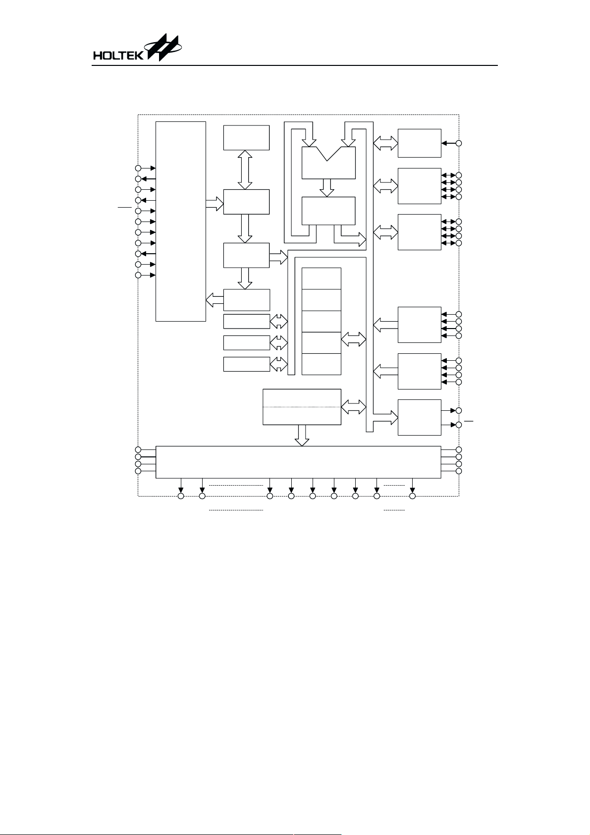
Block Diagram
HTG12B0
XIN
XOUT
OSCI
OSCO
RES
TEST1
TEST2
T1D
T512
VDD
VSS
C ontrol
&
Tim ing
Circuit
Stack
Program
C ounter
ROM
In stru ction
D ecoder
ROM B
RAMB
LC D C
Tem porary
D ata R AM
D isplay D ata R AM
R0
R1
R2
R3
R4
ALU
ACC
Tim er
PA
PB
PS
PM
Sound
Effect
TM C LK
PA0
PA1
PA2
PA3
PB0
PB1
PB2
PB3
PS0
PS1
PS2
PS3
PM 0
PM 1
PM 2
PM 3
BZ
BZ
VOUT1
VOUT2
VOUT3
VOUT4
SEG 0
Note: ACC: Accumulator
R0~R4: Working registers
ROMB: ROM bank switch
RAMB: RAM bank switch
LCDC: LCD control register
PA, PB: I/O ports
PS, PM: Input ports
VLC 1
LC D Driver
SEG 1
SEG 38
SEG 39
COM 1
COM 0
COM 3
COM 2
COM 15
VLC 2
VLC 3
VLC 4
2 September 8, 1999
Page 3
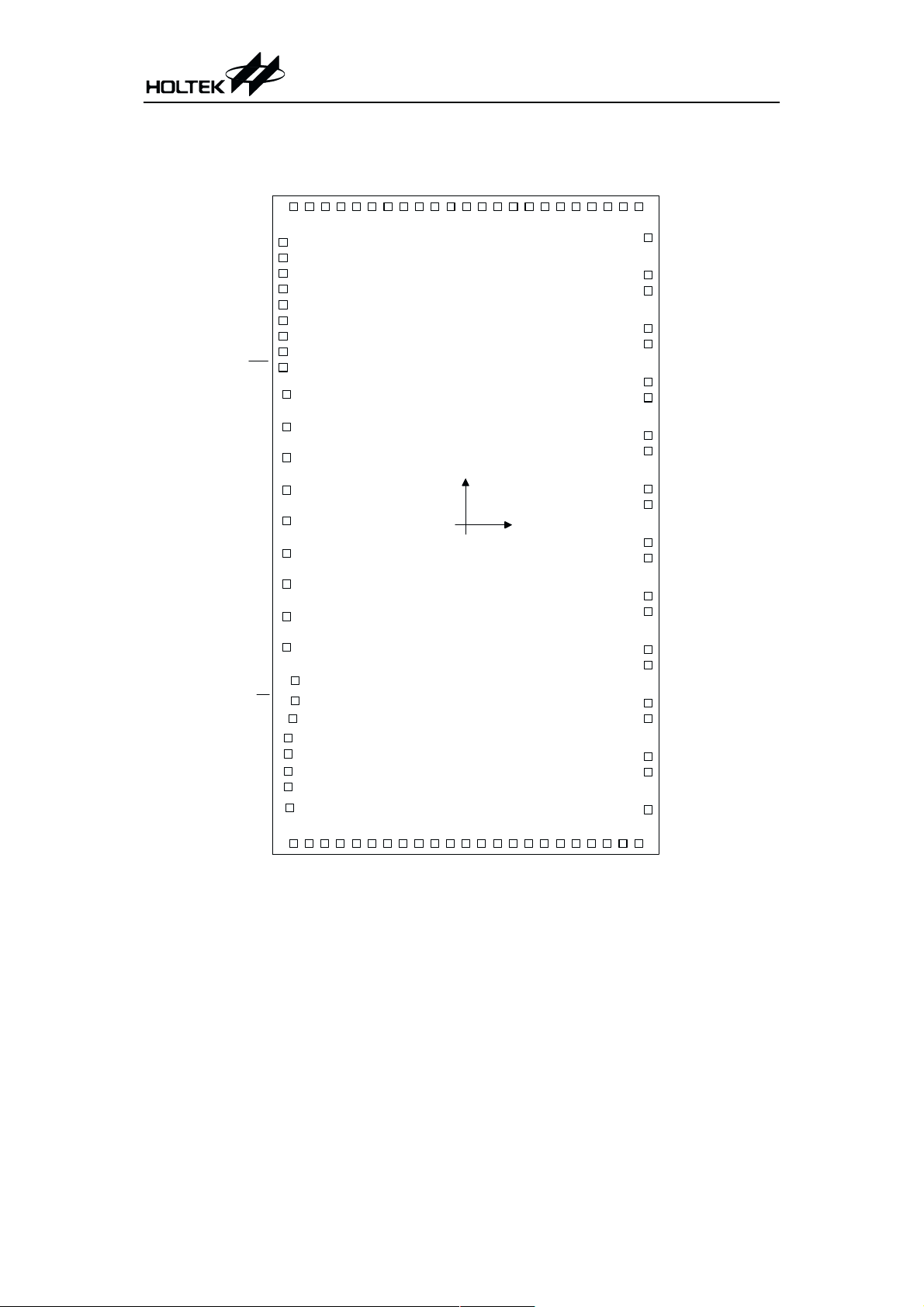
Pad Assignment
HTG12B0
SEG 18
SEG 17
SEG 16
SEG 15
SEG 14
SEG 13
SEG 12
SEG 11
TEST2
TEST1
T512
PM 3
SEG 1
SEG 0
SEG 4
SEG 3
SEG 2
SEG 7
SEG 6
SEG 5
SEG 10
SEG 9
SEG 8
PM 2
PM 1
PM 0
PS3
PS2
PS1
PS0
TM CLK
RES
PB3
PB2
PB1
PB0
PA0
PA1
PA2
PA3
T1D
VDD
OSCO
OSCI
XOUT
XIN
VSS
BZ
BZ
94
1
2
3
4
5
6
7
8
9
10
11
12
13
14
15
16
17
18
19
20
21
22
23
24
25
(0 , 0 )
722673277428752976307731783279808182833784388539864087418842894390449145924693
71
SEG 19
70
SEG 20
69
SEG 21
68
SEG 22
67
SEG 23
66
SEG 24
65
SEG 25
64
SEG 26
63
SEG 27
62
SEG 28
61
SEG 29
60
SEG 30
59
SEG 31
58
SEG 32
57
SEG 33
56
SEG 34
55
SEG 35
54
SEG 36
53
SEG 37
52
SEG 38
51
SEG 39
50
COM 0
33
35
36
VLC1
VLC2
VLC3
VLC4
VOUT1
34
VOUT2
VOUT3
VOUT4
COM 15
COM 14
COM 13
COM 12
COM 11
COM 10
COM 9
COM 8
Chip size: 3060 ´ 5140 (mm)
COM 7
COM 6
COM 5
COM 4
2
49
47
48
COM 3
COM 2
COM 1
* The IC substrate should be connected to VSS in the PCB layout artwork.
3 September 8, 1999
Page 4
HTG12B0
Pad Coordinates
Pad No. X Y Pad No. X Y Pad No. X Y
65 1398.48 972.60
66 1398.48 1092.60
67 1398.48 1381.40
68 1398.48 1501.40
69 1398.48 1790.20
70 1398.48 1910.20
71 1398.48 2199.00
72 1327.44 2436.28
73 1207.44 2436.28
74 1087.44 2436.28
75 967.44 2436.28
76 847.44 2436.28
77 727.44 2436.28
78 607.44 2436.28
79 487.44 2436.28
80 367.44 2436.28
81 247.44 2436.28
82 127.44 2436.28
83 7.44 2436.28
84
85
86
87
88
89
90
91
92
93
94
-112.56
-232.56
-352.56
-472.56
-592.56
-712.56
-832.56
-952.56
-1072.56
-1192.56
-1312.56
10
11
12
13
14
15
16
17
18
19
20
21
22
23
24
25
26
27
28
29
30
31
32
1
-1394.56
2
-1394.56
3
-1394.56
4
-1394.56
5
-1394.56
6
-1394.56
7
-1394.56
8
-1394.56
9
-1394.56
-1368.40
-1368.40
-1368.40
-1368.40
-1368.40
-1368.40 -217.16
-1368.40 -451.88
-1368.40 -700.68
-1368.40 -935.40
-1304.07 -1189.85
-1304.07 -1344.25
-1318.48 -1483.72
-1355.04 -1630.76
-1355.04 -1750.76
-1355.04 -1885.00
-1355.04 -2005.00
-1343.84 -2164.44
-1315.52 -2436.28
-1195.52 -2436.28
-1075.52 -2436.28
-955.52 -2436.28
-835.52 -2436.28
-715.52 -2436.28
2163.72 33 1204.48
2043.72 34 1324.48
1923.72 35 1398.48
1803.72 36 1398.48
1683.72 37 1398.48
1563.72 38 1398.48
1443.72 39 1398.48
1323.72 40 1398.48
1203.72 41 1398.48
998.68 42 1398.48
749.88 43 1398.48
515.16 44 1398.48
266.36 45 1398.48
31.64 46 1398.48
47 1398.48
48 1398.48
49 1398.48
50 1398.48
51 1398.48
52 1398.48
53 1398.48
54 1398.48
55 1398.48
56 1398.48
57 1398.48
58 1398.48
59 1398.48
60 1398.48
61 1398.48 155.00
62 1398.48 275.00
63 1398.48 563.80
64 1398.48 683.80
-2436.28
-2436.28
-2436.28
-2436.28
-2436.28
-2436.28
-2436.28
-2436.28
-2436.28
-2436.28
-2436.28
-2436.28
-2436.28
-2436.28
-2436.28
-2436.28
-2436.28
-2177.80
-1889.00
-1769.00
-1480.20
-1360.20
-1071.40
-951.40
-662.60
-542.60
-253.80
-133.80
Unit: mm
2436.28
2436.28
2436.28
2436.28
2436.28
2436.28
2436.28
2436.28
2436.28
2436.28
2436.28
4 September 8, 1999
Page 5
Pad Description
HTG12B0
Pad No. Pad Name I/O
4~7
94, 1~3
8 TMCLK I
9 RES
17~14
10~13
19, 20 BZ, BZ
21 VDD I
23
22
25
24
26 VSS I
27~30 VLC1~VLC4 I
31~34 VOUT1~VOUT4 I
35~50 COM15~COM0 O
51~90 SEG39~SEG0 O
93
18
92
91
PS3~PS0
PM3~PM0
PA3~PA0
PB3~PB0
OSCI
OSCO
XIN
XOUT
T512
T1D
TEST1
TEST2
I
I
I/O
O Note 1 Sound effect outputs
I
O
I
O
O
O
I
I
Mask
Option
Pull-high or
None.
Note 2
Pull-high
or None.
Note 4
¾
CMOS or
NMOS with
Pull-high or
None.
Note 3
¾
¾
¾
¾
¾
¾
¾
¾
Description
Input pins for input only
Input for TIMER clock
TIMER can be clocked by an external clock or an
internal frequency source.
Input to reset an internal LSI
Reset is active on logical low level.
Input/output pins
Positive power supply
An external resistor between OSCI and OSCO is
needed for internal system clock.
32768Hz crystal oscillator for time base, LCD
clock
Negative power supply, GND
LCD system power 1/4 bias generated
LCDsystemvoltage booster condenserconnecting
terminal
Output for LCD panel common plate
LCD driver outputs for LCD panel segment
For test mode only
TEST1 and TEST2 are left open when the chip is
in normal operation (with an internal pull-high
resistor).
Note: 1. The system clock provides six different sources selectable by mask option to drive the
sound effect clock. If the Holtek sound library is used, only 128K and 64K are acceptable.
2. Each bit of ports PM, PS can be a trigger source of the HALT interrupt, selectable by
mask option.
3. Each bit of ports PA, PB can be selected as CMOS for output pin only, or as NMOS for
I/O pin with pull-high resistor or none by mask option.
4. 14 internal clock sources can be selected by mask option to drive TMCLK. Note that
TMCLK should not be connected to a pull high resistor if an internal source is used.
5 September 8, 1999
Page 6
Absolute Maximum Ratings
HTG12B0
Supply Voltage ..............................-0.3V to 5.5V
Storage Temperature.................-50°Cto125°C
Input Voltage ......................V
-0.3 to VDD+0.3
SS
Operating Temperature ..................0°Cto70°C
Note: These are stress ratings only. Stresses exceeding the range specified under ²Absolute Maxi
mum Ratings² may cause substantial damage to the device. Functional operation of this device
at other conditions beyond those listed in the specification is not implied and prolonged expo
sure to extreme conditions may affect device reliability.
D.C. Characteristics
Ta=25°C
Test Conditions
Symbol Parameter
V
DD
I
DD
Operating Voltage
Operating Current 3V
V
DD
Conditions
¾¾
No load,
=512kHz
f
SYS
Min. Typ. Max. Unit
2.4 3 3.6 V
¾
200 300
mA
Standby Current,
I
STB
(f
OFF and RTC ON,
SYS
3V Halt mode
¾
10 15
mA
LCD ON)
V
V
I
I
I
I
R
V
IL
IH
OL1
OH1
OL2
OH2
PH
LCD
Input Low Voltage 3V
Input High Voltage 3V
PA, PB, BZ and BZ
Output Sink Current
PA, PB, BZ and BZ
Output Source Current
Segment Output Sink
Current
Segment Output Source
Current
3V
3V
3V
3V
Pull-high Resistor 3V
V
Output Voltage
LCD
3V
¾
¾
=0.3V
V
OL
=2.7V
V
OH
VOL=0.44V
V
=4.4V
LCD
VOH=4.0V
V
=4.4V
LCD
PS, PM, RES
TMCLK
¾
0.8V
0
DD
¾
¾
1.5 3
-0.5 -1 ¾
100 200
30 60
,
50 100 150
3.96 4.4 4.84 V
0.2V
DD
V
DD
¾
¾mA
¾mA
V
V
mA
mA
kW
-
-
6 September 8, 1999
Page 7
HTG12B0
A.C. Characteristics
Symbol Parameter
f
SYS
t
CY
f
TIMER
t
RES
f
SOUND
System Clock 3V
Cycle Time 3V
Timer I/P Frequency
(TMCLK)
Reset Pulse Width
Sound Effect Clock
*: Only these two clocking signal frequencies are supported by the Holtek sound library.
Test Conditions
V
DD
Conditions
R=620kW~51kW
f
=1MHz
SYS
3V
¾
¾¾
¾¾ ¾
Min. Typ. Max. Unit
128
¾
0
5
*64 or 128
¾
4
¾
1000 kHz
¾ms
1000 kHz
¾¾
¾
Functional Description
·
Program counter - PC
This counter addresses the program ROM and
is arranged as a 12-bit binary counter from PC0
to PC11 whose contents specify a maximum of 4096
addresses. The program counter counts with an
increment of 1 or 2 with each execution of an instruc
tion.
When executing the jump instruction (JMP,
JNZ, JC, JTMR,...), a subroutine call, initial reset, internal interrupt, RTC interrupt or returning from a subroutine, the program
counter is loaded with the corresponding instruction data as shown in the table.
Note: P0~P11: Instruction code
@: PC11 keeps current value
S0~S11: Stack register bits
ROMB0 and ROMB1 are set to 0 at
power on reset.
Program memory - ROM
The program memory is the executable memory
and is arranged in a 4096´8-bit format. There
are four banks for program memory in
HTG12B0, each bank shown in the figure can be
switched by assigning ROMB0 and ROMB1 (bit0
and bit1 of ROMB). ROMB is the ROM bank
pointer and can be written only by executing
²MOV ROMB, A² instruction. Bit 2 and bit 3 of
ROMB are unused bits. The address is specified
by the program counter (PC). Four special loca
tions are reserved as described next.
-
-
Location 000H: (Bank 0)
Activating the processor RES
pin causes the
first instruction to be fetched from location 0.
000H
004H
008H
00BH
F00H
FFFH
R e s e t in itia l p r o g r a m
Tim er interrupt subroutine
R T C interrupt subroutine
Page N look-up table
Page F look-up table (256 bytes)
8 bits
Program memory ROMB=XX00B
000H
004H
008H
00BH
F00H
FFFH
Tim er interrupt subroutine
R T C interrupt subroutine
Page N look-up table
Page F look-up table (256 bytes)
8 bits
Program memory ROMB=XX01B
Ta=25°C
ms
kHz
Program
ROM
Bank 0
Program
ROM
Bank 1
7 September 8, 1999
Page 8
HTG12B0
·
Location 004H: (Bank 0~3)
Contains the timer interrupt resulting from a
TIMER overflow. If the interrupt is enabled, the
CPU begins execution at location 004H.
·
Location 008H: (Bank 0~3)
Activating the RTC of the processor with the
interrupts enabled causes the program to
jump to this location.
·
Locations n00H to nFFH: (Bank 0~3)
Each page in the program memory consists of
256 bytes. This area from n00H to nFFH and
F00H to FFFH can be used as a look-up table.
Instructions such as READ R4A, READ
MR0A, READF R4A, READF MR0A can read
the table and transfer the contents of the ta
ble to ACC and R4 or to ACC and a data mem
ory address specified by the register pair
R1,R0. However as R1,R0 can only store 8
bits, these instructions cannot fully specify
the full 12 bit program memory address. For
this reason a jump instruction should first be
used to place the program counter in the right
page. The above instructions can then be used
to read the look up table data.
Note that the page number n must be greater
than zero since some locations in page 0 are reserved for specific usage. This area may function as normal program memory.
The program memory mapping is shown in the
diagram.
Mode
Initial
reset
Internal
interrupt
RTC
interrupt
Jump, call
instruction
Conditional
branch
Return from
subroutine
PC13 PC12 PC11 PC10 PC9 PC8 PC7 PC6 PC5 PC4 PC3 PC2 PC1 PC0
ROMB1 ROMB0 000000000000
ROMB1 ROMB0 000000000100
ROMB1 ROMB0 000000001000
ROMB1 ROMB0 P11 P10 P9 P8 P7 P6 P5 P4 P3 P2 P1 P0
ROMB1 ROMB0 @ P10 P9 P8 P7 P6 P5 P4 P3 P2 P1 P0
ROMB1 ROMB0 S11 S10 S9 S8 S7 S6 S5 S4 S3 S2 S1 S0
In the execution of an instruction, the program
counter is added before the execution phase, so
careful manipulation of READ MR0A and
READ R4A is required in the page margin.
000H
004H
008H
00BH
F00H
FFFH
-
Tim er interrupt subroutine
R T C interrupt subroutine
Page N look-up table
Page F look-up table (256 bytes)
8 bits
Program memory ROMB=XX10B
-
000H
004H
008H
00BH
F00H
FFFH
Tim er interrupt subroutine
R T C interrupt subroutine
Page N look-up table
Page F look-up table (256 bytes)
8 bits
Program memory ROMB=XX11B
Program Counter
Program
ROM
Bank 2
Program
ROM
Bank 3
Program memory
8 September 8, 1999
Page 9

HTG12B0
R A M B ank 1
(RAM B=X001B)
Tem porary D ata A rea
00H
Tem porary D ata A rea
7FH
R A M B ank 0
(RAM B=X000B)
(128 x 4)
4 bits
00H
7FH
Temporary data memory
Stack register
The stack register is a group of registers used to
save the contents of the program counter (PC)
and is arranged into 13 bits ´ 1 level. One bit is
used to store the carry flag. An interrupt will
force the contents of the PC and the carry flag
onto the stack register. A subroutine call will
also cause the PC contents to be pushed onto
the stack; however the carry flag will not be
stored. At the end of a subroutine or an inter
rupt routine which is signaled by a return in
struction, RET or RETI restore the program
counter to its previous value from stack regis
ter. Executing ²RETI² instruction will restore
the carry flag from the stack register, but
²RET² does not.
Working registers - R0, R1, R2, R3, R4
There are five working registers (R0, R1, R2, R3,
R4) usually used to store the frequently accessed
intermediate results. Using the instructions INC
Rn and DEC Rn the working registers can increment (+1) or decrement (-1). The JNZ Rn (n=0, 1,
4) instruction makes efficient use of the working
registers as a program loop counter. Also the register pairs R0,R1 and R2,R3 are used as a data
memory pointer when the memory transfer instruction is executed.
Data memory - RAM
The static data memory (RAM) is arranged in
128´4-bit format and is used to store data. All
of the data memory locations are indirectly
addressable through the register pair R1,R0 or
R3,R2; for example MOV A,[R3R2] or MOV
[R3R2],A.
There are two areas in the data memory, the
temporary data area and display data area. Ac
cess to the temporary data area is from 00H to
R A M B ank 7
(RAM B=X111B)
00H
(128 x 4)
4 bits
Tem porary D ata A rea
7FH
(128 x 4)
4 bits
7FH of RAM bank 0~RAM bank 7. Access to the
display data area is from B0H to FFH of LCD
bank 0 and bank 1.
There are eight banks for the temporary data
memory in HTG12B0, each bank shown in the
figure can be switched by assigning
RAMB0~RAMB2 (bit 0~bit 2 of RAMB). RAMB
is the RAM bank pointer and can be written
only by executing ²MOV RAMB, A² instruction.
Bit 3 of RAMB is unused bit. Each bank maps to
different area of the data memory.
-
There are two banks for displaying the data
memory, each bank can be switched by the as
signment of LCDC0 (bit 0 of LCDC). LCDC is a
control register for LCD application and can be
written only by executing ²MOV LCDC, A² in
struction.
When data is written into the display data area,
it is automatically read by the LCD driver
which then generates the corresponding LCD
driving signals.
LC D B ank 0
(LCDC =XXX0B)
B0H
FFH
B0H
FFH
D isplay D ata Area
(80 x 4)
4 bits
LC D B ank 1
(LC DC =XXX1B)
D isplay D ata Area
(80 x 4)
4 bits
Display data memory
-
-
-
9 September 8, 1999
Page 10
HTG12B0
The locations between the temporary and
display data areas are undefined and cannot be
used.
Accumulator - ACC
The accumulator is the most important data
register in the processor. It is one of the sources
of input to the ALU and the destination of the
results of the operations performed in the ALU.
Data to and from the I/O ports and memory also
passes through the accumulator.
Arithmetic and logic unit - ALU
This circuit performs the following arithmetic
and logic operations ...
·
Add with or without carry
·
Subtract with or without carry
·
AND, OR, Exclusive-OR
·
Rotate right, left through carry
·
BCD decimal adjust for addition
·
Increment, decrement
·
Data transfers
·
Branch decisions
The ALU not only outputs the results of data
operations, but also sets the status of the carry
flag (CF) in some instructions.
Timer/counter
The HTG12B0 contains a programmable 8-bit
count-upcounter which can be used to count external
events or used as a clock to generate an accurate
time base.
If the 8-bit timer clock is supplied by an exter
nal source from pin TMCLK, synchronization
problems may occur when reading the data
from the timer. It is therefore recommended
that the timer is stopped before retrieving the
data. The 8-bit counter will increment on the
rising edge of the clock whether it is internally
or externally generated.
The Timer/Counter may be set and read with
software instructions and stopped by a hard
ware reset or a TIMER OFF instruction. To re
start the timer, load the counter with the value
XXH and then issue a TIMER ON instruction.
Note that XX is the desired start count immedi
ate value of the 8 bits. Once the Timer/Counter
is started it increments to a maximum count of
FFH and then overflows to zero (00H). It then
continues to count until stopped by a TIMER
OFF instruction or a reset.
The increment from the maximum count of
FFH to a zero (00H) triggers a timer flag TF
and an internal interrupt request. The inter
rupt may be enabled or disabled by executing
the EI and DI instructions. If the interrupt is
enabled, the timer overflow will cause a subrou
tine call to location 4. The state of the timer flag
can also be tested with the conditional jump in
struction JTMR. The timer flag is cleared after
the interrupt or the JTMR instruction is exe
cuted.
If an internal source is used, the frequency is
determined by the system clock and the param
eter n as defined in the equation. The frequency
of the internal frequency source can be selected
by mask option.
Frequency of TIMER clock =
system clock
where n=0, 1, 2... 3 selectable by mask option.
RTC
There is a real time clock (RTC) function implemented on the HTG12B0. The RTC function is
used to generate an accurate time period. The
RTC circuit clock source comes from the 32768Hz
crystal oscillator. The block diagram is shown as
follows.
-
X'tal 32768H z
1
128
1
, n=0~7
n
2
M ask O ptio n
The output of RTC can be selected by mask op
tion.
256
Frequency of RTC output =
-
The RTC output is used to generate an inter
-
rupt signal.
n
2
, n=0~7
n
2
In te rru p t
-
-
-
-
-
-
-
-
10 September 8, 1999
Page 11

HTG12B0
Interrupt
The HTG12B0 provides both TIMER and RTC
interrupt modes. The DI and EI instructions
are used to disable and enable the interrupts.
When the RTC is activated during enable inter
rupt mode and the program is not within a
CALL subroutine, this causes a subroutine call
to location 8 and reset the interrupt latch.
Likewise when the timer flag is set in the en
able interrupt mode and the program is not
within a CALL subroutine, the TIMER inter
rupt is activated. This cause a subroutine call to
location 4 and resets the timer flag. If both
TIMER and RTC interrupts arrive at the same
time, the RTC one will be serviced first.
When running under a CALL subroutine or DI
the interrupt acknowledge is on hold until the
RET or EI instruction is invoked. The CALL in
struction should not be used within an inter
rupt routine as unpredictable results may
occur. If within a CALL subroutine both
TIMER and RTC interrupt occur, no matter
what order they arrive in, the RTC interrupt
will be serviced first after leaving the CALL
subroutine. This also applies if the two interrupt arrive at the same time.
The interrupts are disabled by a hardware reset or a DI instruction. They remain disabled
until the EI instruction is executed.
Initial reset
The HTG12B0 provides a RES
pin for system
initialization. This pin is equipped with an internal pull high resistor and in combination
with an external 0.1m~1mF capacitor, it provides an internal reset pulse of sufficient length
to guarantee a reset to all internal circuits. If
the reset pulse is generated externally, the RES
pin must be held low at least 5ms.
When RES
is active, the internal block will be
initialized as shown below:
PC 000H
TIMER Stop
-
Timer flag Reset (low)
SOUND
-
Sound off and One sing
mode
Output port A High (or floating state)
LCD output Enable
BZ and BZ
output Low level
ROMB XX00B
RAMB X000B
LCDC 1100B
-
-
HALT
This is a special feature of the HTG12B0 to inter
rupt the chip¢s normal operation and reduce
power consumption. When a HALT is executed
the following happens ...
·
The system clock will be stopped
·
The contents of the on-chip RAM and registers remain unchanged
·
RTC oscillator keeps on running
·
BZ and BZ maintain low level output
The system can leave the HALT mode through
initial reset or RTC interrupt or wake-up from
the following entry of program counter value.
Initial reset: 00H
Wake-up: next address of the HALT instruction
-
11 September 8, 1999
Page 12

HTG12B0
When the halt status is terminated by the RTC
interrupt, the following procedure takes place:
Case 1: If the system is in an interrupt-disable
state before entering the halt state:
·
The system will be awakened and returns to
the main program instruction following the
HALT command.
·
The RTC interrupt will be held until the sys
tem receives an enable interrupt command by
which the RTC interrupt will be serviced.
Case 2: If the system is in an interrupt enable
state:
·
The RTC interrupt will awake the system and
execute the RTC interrupt subroutine.
In the HALT mode, each bit of ports PM, PS,
can be used as wake-up signal by mask option
to wake-up the system. This signal is active in
low-going transition.
Sound effects
The HTG12B0 includes sound effect circuitry
which offers up to 16 sounds with 3 tones, boom
and noise effects. Holtek supports a sound li
brary including melodies, alarms, machine
guns etc..
If the instruction ²SOUND A² is executed, the
specified sound begins. Each time ²SOUND
OFF² is executed, it terminates the singing
sound immediately.
There are two singing modes, SONE mode and
SLOOP mode activated by SOUND ONE and
SOUND LOOP. In SONE mode the specified
sound plays only once. In the SLOOP mode the
specified sound keeps re-playing.
Since sounds 0~11 contain 32 notes and sounds
12~15 include 64 notes the latter possesses
better sound than the former.
The frequency of the sound effect circuit can be
selected by mask option.
Frequency of sound effect circuit =
system clock
m
2
...where m=0,1,2,3,4,5.
Holtek¢s sound library supports only sound
clock frequency of 128K or 64K. To use Holtek¢s
sound library the proper system clock and
mask option should be selected.
LCD display memory
As mentioned in the data memory section, the
LCD display memory is embedded in the data
-
memory. It can be read and written to in the
same way as normal data memory.
The figure illustrates the mapping between the
display memory and LCD pattern for the
HTG12B0.
There is an ON/OFF switch for display con
trolled by bit 3 of LCDC (LCDC 3). The corre
sponding bit of the LCDC 3 represents ²ON² or
²OFF² of display of LCD display memory.
The LCD display module may have any form as
long as the number of commons does not exceed
16 and the number of segments is not over 40.
DISPLAY M EM O R Y
FEH FC H FA H
-
0
1
2
3
4
5
6
7
SEGM ENT
FFH
FDH FB H
0 3 38 39
F8H
F9H
B4H B2H B0H BITCOM
B5H B3H B1H
3721
LCD display memory (LCDC0=0)
-
-
0
1
2
3
0
1
2
3
12 September 8, 1999
Page 13

HTG12B0
DISPLAY M EM O R Y
8
9
10
11
12
13
14
15
SEGM ENT
FEH FCH FAH
FFH
FDH FBH
0 3 38 39
F8H
F9H
B4H B2H B0H BITCOM
0
1
2
3
B5H B3H B1H
0
1
2
3
3721
LCD display memory (LCDC0=1)
LCD driver output
All of the LCD segments are random after an
initial clear. The bias voltage circuits of the
LCD display is built-in and no external resistor
is required.
The output number of the HTG12B0 LCD
driver is 40´16 which can directly drive an LCD
with 1/16 duty cycle and 1/4 bias.
The frequency of the LCD driving clock source
can be selected from RTC OSC or system clock
by accessing bit 1 of LCDC.
There are many frequency division of the LCD
clock which can be selected by mask option ei
ther from RTC OSC or system clock.
·
RTC OSC
16384
Frequency of LCD clock =
Hz
n
2
....where n=0~7
·
System clock
f64
Frequency of LCD clock =
SYS
n
2
....where n=0~5
LCD driver output can be enabled or disabled
by setting LCDC 3 without the influence of the
related memory condition.
LCD driver output is enabled by setting LCDC3
as ²1², and disabled by setting LCDC 3 as ²0².
Register Bit No. Function
Select LCD bank
0
0=Bank 0 (Com0~7)
1=Bank 1 (Com8~15)
Select LCD clock source
1
0=RTC OSC (32768Hz)
1=System clock
LCDC
PM3 edge latch control bit
2
1=Enabled
0=Disabled
Control LCD display
3
0=OFF
1=ON
LCDC Register
An example of an LCD driving waveform (1/16
duty and 1/4 bias) is shown below.
1 2 3 13 14 15 1 2 3 4
1024H z
VLCD
3/4V LC D
COM 0
2/4V LC D
1/4V LC D
GND
COM 1
SEG0
VLCD
3/4V LC D
2/4V LC D
1/4V LC D
GND
VLCD
3/4V LC D
2/4V LC D
1/4V LC D
GND
-
VLCD is fixed at 4.4V when V
64H z
is from 2.4V to
DD
3.6V.
Hz
5
13 September 8, 1999
Page 14

HTG12B0
Oscillator
Only one external resistor is required for the
HTG12B0 system clock.
The system clock is also used as the reference
signal of the sound effect clock or internal fre
quency source of the TIMER.
Another crystal oscillator is needed for use as
the reference signal of the LCD driving clock
and RTC interrupt clock source.
A machine cycle consists of a sequence of 4
states numbered T1 to T4. Each state lasts for
one oscillator period. The machine cycle is 4msif
the system frequency is up to 1MHz.
OSCI
R
OSCO
XIN
32.768kH z
XOUT
RC and RTC oscillator
Interfacing
The HTG12B0 microcontrollers communicate
with the outside world through two input pins
PS and PM and two output pins PA and PB.
Input ports - PS, PM
All of the ports can have internal pull high resistors determined by mask option. Every bit of
the input ports PS and PM can be specified as a
trigger source for waking up the HALT interrupt by mask option. Ahigh to low transition on
one of these pins will wake up the device from a
HALT status.
V
DD
P u ll- h ig h
-
mask
option
Wake-up
mask
option
Internal bus
Input ports PS, PM
PM3 has a falling edge latch function selected
by mask option. Once the falling edge signal is
latched, it will remain in its state until the clear
instruction is executed by setting bit 2 of LCDC
from high to low.
Input/output port - PA, PB
PA and PB can be used for input/output or out
put operation by selecting NMOS or CMOS
mask option respectively, and each bit can be
configured with or without pull-high resistor
when the NMOS is selected. If the NMOS is se
lected, it should be noted that, before reading,
data from pads should output ²1² to the related
bits to disable the NMOS device.
V
DD
Internal bus
Q
D
Q
CK
R ead control
M ask op tion
Wake-up
R ead control
-
-
Pull-high
M ask op tion
Input/output port PA, PB
14 September 8, 1999
Page 15

HTG12B0
Mask options
HTG12B0 provides the following mask option
for different applications.
·
Each bit of input ports PS, PM with pull-high
resistor
·
Each bit of input ports PS, PM function as
HALT wake-up trigger.
·
Each bit of input/output port PA, PB with
CMOS or NMOS with pull-high or none.
·
8-bit programmable TIMER with internal or
external frequency sources. There are 14 in
ternal frequency sources which can be se
lected as a clocking signal.
If using internal frequency sources as
clocking signal TMCLK cannot connect with
pull-high resistor.
·
Six kinds of sound clock frequencies:
f
/2m, m=0, 1, 2, 3, 4, 5
SYS
·
There are eight kinds of RTC interrupt fre
quencies. RTC interrupt frequency=256/2
-
n
Hz,
n=0~7.
·
LCD clock source division:
If RTC OSC is selected, the frequency of LCD
clock=16384/2
n
Hz, n=0~7.
If system clock is selected, the frequency of
f64
LCD clock=
-
·
PM3 falling edge latch function.
SYS
n
2
Hz, n=0~5.
-
15 September 8, 1999
Page 16

Application Circuits
HTG12B0
R*
X'
ta l
PB0
PB1
PB2
PB3
PA0
PA1
PA2
PA3
PM 0
PM 1
PM 2
PM 3
PS0
PS1
PS2
PS3
I/O
PORT
IN P U T
PORT
IN P U T
PORT
OSCI
OSCO
XIN
XOUT
I/O
PORT
06/ *
COM 0
COM 1
COM 15
SEGM EN T
OUTPUT
BZ
BZ
RES
VOUT1
VOUT2
VOUT3
VOUT4
VLC 1
VLC 2
VLC 3
VLC 4
X40
0.1mF
LC D
P a tte rn
(1 /4 B ia s,
1/16 D uty)
Piezo
Buzzer
R *: D epe nds on the required system clock frequency. (R =620kW~51kW, a t VDD=3V)
X'tal: R ealtim e clock frequency. (X 'tal=32768H z)
16 September 8, 1999
Page 17

Instruction Set Summary
Mnemonic Description Byte Cycle CF
Arithmetic
ADD A,[R1R0]
ADC A,[R1R0]
SUB A,[R1R0]
SBC A,[R1R0]
ADD A,XH
SUB A,XH
DAA
Logic Operation
AND A,[R1R0]
OR A,[R1R0]
XOR A,[R1R0]
AND [R1R0],A
OR [R1R0],A
XOR [R1R0],A
AND A,XH
OR A,XH
XOR A,XH
Increment and
Decrement
INC A
INC Rn
INC [R1R0]
INC [R3R2]
DEC A
DEC Rn
DEC [R1R0]
DEC [R3R2]
Data Move
MOV ROMB, A
MOV RAMB, A
MOV LCDC, A
MOV A,Rn
MOV Rn,A
MOV A,[R1R0]
MOV A,[R3R2]
MOV [R1R0],A
MOV [R3R2],A
MOV A,XH
MOV R1R0,XXH
MOV R3R2,XXH
MOV R4,XH
Add data memory to ACC
Add data memory with carry to ACC
Subtract data memory from ACC
Subtract data memory from ACC with borrow
Add immediate data to ACC
Subtract immediate data from ACC
Decimal adjust ACC for addition
AND data memory to ACC
OR data memory to ACC
Exclusive-OR data memory to ACC
AND ACC to data memory
OR ACC to data memory
Exclusive-OR ACC to data memory
AND immediate data to ACC
OR immediate data to ACC
Exclusive-OR immediate data to ACC
Increment ACC
Increment register, n=0~4
Increment data memory
Increment data memory
Decrement ACC
Decrement register, n=0~4
Decrement data memory
Decrement data memory
MOV ACC to ROMB
MOV ACC to RAMB
MOV ACC to LCDC
Move register to ACC, n=0~4
Move ACC to register, n=0~4
Move data memory to ACC
Move data memory to ACC
Move ACC to data memory
Move ACC to data memory
Move immediate data to ACC
Move immediate data to R1 and R0
Move immediate data to R3 and R2
Move immediate data to R4
1
1
1
1
2
2
1
1
1
1
1
1
1
2
2
2
1
1
1
1
1
1
1
1
1
1
1
1
1
1
1
1
1
1
2
2
2
HTG12B0
1
1
1
1
2
2
1
1
1
1
1
1
1
2
2
2
1
1
1
1
1
1
1
1
1
1
1
1
1
1
1
1
1
1
2
2
2
Ö
Ö
Ö
Ö
Ö
Ö
Ö
¾
¾
¾
¾
¾
¾
¾
¾
¾
¾
¾
¾
¾
¾
¾
¾
¾
¾
¾
¾
¾
¾
¾
¾
¾
¾
¾
¾
¾
¾
17 September 8, 1999
Page 18

HTG12B0
Mnemonic Description Byte Cycle CF
Rotate
RL A
RLC A
RR A
RRC A
Input & Output
IN A,Pi
OUT Pi,A
Branch
JMP addr
JC addr
JNC addr
JTMR addr
JAn addr
JZ A,addr
JNZ A,addr
JNZ Rn,addr
Subroutine
CALL addr
RET
RETI
Flag
CLC
STC
EI
DI
NOP
Timer
TIMER XXH
TIMER ON
TIMER OFF
MOV A,TMRL
MOV A,TMRH
MOV TMRL,A
MOV TMRH,A
Table Read
READ R4A
READ MR0A
READF R4A
READF MR0A
Rotate ACC left
Rotate ACC left through carry
Rotate ACC right
Rotate ACC right through carry
Input port-i to ACC ,port-i=PM, PS, PA, PB
Output ACC to port-i, port-i=PA, PB
Jump unconditionally
Jump on carry=1
Jump on carry=0
Jump on timer overflow
Jump on ACC bit n=1
Jump on ACC is zero
Jump on ACC is not zero
Jump on register Rn not zero, n=0,1,4
Subroutine call
Return from subroutine or interrupt
Return from interrupt service routine
Clear carry flag
Set carry flag
Enable interrupt
Disable interrupt
No operation
Set 8 bits immediate data to TIMER
Set TIMER start counting
Set TIMER stop counting
Move low nibble of TIMER to ACC
Move high nibble of TIMER to ACC
Move ACC to low nibble of TIMER
Move ACC to high nibble of TIMER
Read ROM code of current page to R4 and ACC
Read ROM code of current page to M(R1,R0), ACC
Read ROM code of page F to R4 and ACC
Read ROM code of page F to M(R1,R0), ACC
1
1
1
1
1
1
2
2
2
2
2
2
2
2
2
1
1
1
1
1
1
1
2
1
1
1
1
1
1
1
1
1
1
1
1
1
1
1
1
2
2
2
2
2
2
2
2
2
1
1
1
1
1
1
1
2
1
1
1
1
1
1
2
2
2
2
Ö
Ö
Ö
Ö
¾
¾
¾
¾
¾
¾
¾
¾
¾
¾
¾
¾
Ö
0
1
¾
¾
¾
¾
¾
¾
¾
¾
¾
¾
¾
¾
¾
¾
18 September 8, 1999
Page 19

HTG12B0
Mnemonic Description Byte Cycle CF
Sound Control
SOUND A
SOUND ONE
SOUND LOOP
SOUND OFF
Miscellaneous
HALT Enter power down mode 2 2
Activate SOUND channel with ACC
Turn on SOUND one cycle
Turn on SOUND repeat cycle
Turn off SOUND
1
1
1
1
1
1
1
1
¾
¾
¾
¾
¾
19 September 8, 1999
Page 20

HTG12B0
Instruction Definition
ADC A,[R1R0] Add data memory contents and carry to accumulator
Machine Code 00001000
Description
Operation
ADD A,XH Add immediate data to accumulator
Machine Code 01000000 0000dddd
Description The specified data is added to the accumulator. Carry is affected.
Operation
ADD A,[R1R0] Add data memory contents to accumulator
Machine Code 00001001
Description
Operation
AND A,XH Logical AND immediate data to accumulator
Machine Code 01000010 0000dddd
Description Data in the accumulator is logically AND with the immediate data speci
Operation
The contents of the data memory addressed by the register pair ²R1,R0²
and the carry are added to the accumulator. Carry is affected.
ACC ¬ ACC+M(R1,R0)+C
ACC ¬ ACC+XH
The contents of the data memory addressed by the register pair ²R1,R0²
is added to the accumulator. Carry is affected.
ACC ¬ ACC+M(R1,R0)
fied by code.
ACC ¬ ACC ²AND² XH
-
AND A,[R1R0] Logical AND accumulator with data memory
Machine Code 00011010
Description Data in the accumulator is logically AND with the data memory ad-
dressed by the register pair ²R1,R0².
Operation
AND [R1R0],A Logical AND data memory with accumulator
Machine Code 00011101
Description
Operation
ACC ¬ ACC ²AND² M(R1,R0)
Data in the data memory addressed by the register pair ²R1,R0² is logi
cally AND with the accumulator
M(R1,R0) ¬ M(R1,R0) ²AND² ACC
20 September 8, 1999
-
Page 21

CALL address Subroutine call
Machine Code 1111aaaa aaaaaaaa
Description
Operation
CLC Clear carry flag
Machine Code 00101010
Description The carry flag is reset to zero.
Operation
The program counter bits 0-11 are saved in the stack. The program coun
ter is then loaded from the directly-specified address.
Stack ¬ PC+2
PC ¬ address
C ¬ 0
HTG12B0
-
DAA
Machine Code 00110110
Description The accumulator value is adjusted to the BCD (Binary Code Decimal)
Operation If ACC>9 or CF=1 then
DEC A Decrement accumulator
Machine Code 00111111
Description Data in the accumulator is decremented by one. Carry flag is not af-
Operation
DEC Rn Decrement register
Machine Code 0001nnn1
Description
Operation
DEC [R1R0] Decrement data memory
Machine Code 00001101
Description
Operation
Decimal-Adjust accumulator
code, if the contents of the accumulator is greater, then 9 or C (Carry flag)
is one.
ACC ¬ ACC+6, C ¬ 1
else
ACC ¬ ACC, C ¬ C
fected.
ACC ¬ ACC-1
Data in the working register ²Rn² is decremented by one. Carry flag is
not affected.
Rn ¬ Rn-1; Rn=R0, R1, R2, R3, R4, for n=0,1,2,3,4
Data in the data memory specified by the register pair ²R1,R0² is decre
mented by one. Carry flag is not affected.
M(R1, R0) ¬ M(R1,R0)-1
-
21 September 8, 1999
Page 22

HTG12B0
DEC [R3R2] Decrement data memory
Machine Code 00001111
Description
Operation
DI Disable interrupt
Machine Code 00100101 00000011
Description Internal time-out interrupt and external interrupt are disabled.
EI Enable interrupt
Machine Code 00100101 00000010
Description Internal time-out interrupt and external interrupt are enabled.
HALT Halt system clock
Machine Code 00110111 00111110
Description Turn off system clock, and enter power down mode.
Operation
IN A,Pi Input port to accumulator
Machine Code 00101100 PA 01001000 PB
Description
Operation
Data in the data memory specified by the register pair ²R3, R2² is decre
mented by one. Carry flag is not affected.
M(R3,R2) ¬ M(R3,R2)-1
PC ¬ (PC)+1
00110010 PM 00110011 PS
The data on port ²Pi² is transferred to the accumulator.
ACC ¬ Pi; Pi=PA, PB, PM or PS
-
INC A Increment accumulator
Machine Code 00110001
Description Data in the accumulator is incremented by one. Carry flag is not affected.
Operation
INC Rn Increment register
Machine Code 0001nnn0
Description
Operation
ACC ¬ ACC+1
Data in the working register ²Rn² is incremented by one. Carry flag is
not affected.
Rn ¬ Rn+1; Rn=R0,R1,R2,R3,R4 for n=0,1,2,3,4
22 September 8, 1999
Page 23

INC [R1R0] Increment data memory
Machine Code 00001100
Description
Operation
INC [R3R2] Increment data memory
Machine Code 00001110
Description
Operation
JAn address Jump if accumulator Bit n is set
Machine Code 100nnaaa aaaaaaaa
Description
Operation
JC address Jump if carry is set
Machine Code 11000aaa aaaaaaaa
Description
Operation
Data in the data memory specified by the register pair ²R1,R0² is incre
mented by one. Carry flag is not affected.
M(R1,R0) ¬ M(R1,R0)+1
Data memory specified by the register pair ²R3, R2² is incremented by
one. Carry flag is not affected.
M(R3,R2) ¬ M(R3,R2)+1
Bits 0-10 of the program counter are replaced with the directly¢specified
address, bit 11 of the program counter and PA3 of memory bank remain,
if accumulator bit n is set to one.
PC (bit 0-10) ¬ address, if ACC bit n=1 (n = 0, 1, 2, 3)
PC ¬ PC+2, if ACC bit n=0
Bits 0-10 of the program counter are replaced with the directly¢specified
address, bit 11 of the program counter and PA3 of memory bank remain,
if the C (Carry flag) is set to one.
PC (bit 0-10) ¬ address, if C=1
PC ¬ PC+2, if C=0
HTG12B0
-
JMP address Direct Jump
Machine Code 1110aaaa aaaaaaaa
Description
Operation
JNC address Jump if carry is not set
Machine Code 11001aaa aaaaaaaa
Description
Operation
Bits 0-11 of the program counter are replaced with the directly¢specified
address.
PC ¬ address
Bits 0-10 of the program counter are replaced with the directly¢specified
address, bit 11 of the program counter and PA3 of memory bank remain,
if the C (Carry flag) is set to zero.
PC (bit 0-10) ¬ address, if C=0
PC ¬ PC+2, if C=1
23 September 8, 1999
Page 24

JNZ A,address Jump if accumulator is not zero
Machine Code 10111aaa aaaaaaaa
Description
Operation
JNZ Rn,address Jump if register is not zero
Machine Code 10100aaa aaaaaaaa R0
Description
Operation
JTMR address Jump if time-out
Machine Code 11010aaa aaaaaaaa
Description
Operation
Bits 0-10 of the program counter are replaced with the directly¢specified
address, bit 11 of the program counter and PA3 of memory bank remain,
if the accumulator is not zero.
PC (bit 0-10) ¬ address, if ACC¹0
PC ¬ PC+2, if ACC=0
10101aaa aaaaaaaa R1
11011aaa aaaaaaaa R4
Bits 0-10 of the program counter are replaced with the directly¢specified
address, bit 11 of the program counter and PA3 of memory bank remain,
if the register is not zero.
PC (bit 0-10) ¬ address, if Rn¹0; Rn=R0, R1, R4
PC ¬ PC+2, if Rn=0
Bits 0-10 of the program counter are replaced with the directly¢specified
address, bit 11 of the program counter and PA3 of the memory bank re
main, if the TF (Timer flag) is set to one.
PC (bit 0-10) ¬ address, if TF=1
PC ¬ PC+2, if TF=0
HTG12B0
-
JZ A,address Jump if accumulator is zero
Machine Code 10110aaa aaaaaaaa
Description
Operation
MOV A,Rn Move register to accumulator
Machine Code 0010nnn1
Description
Operation
Bits 0-10 of the program counter are replaced with the directly¢specified
address, bit 11 of the program counter and PA3 of the memory bank remain, if the accumulator is zero.
PC (bit 0-10) ¬ address, if ACC=0
PC ¬ PC+2, if ACC¹0
Data in the working register ²Rn² is moved to the accumulator.
ACC ¬ Rn; Rn=R0, R1, R2, R3, R4, for n=0,1,2,3,4
24 September 8, 1999
Page 25

HTG12B0
MOV A,TMRH Move timer to accumulator
Machine Code 00111011
Description The high nibble data of the Timer counter is loaded to the accumulator.
Operation
MOV A,TMRL Move timer to accumulator
Machine Code 00111010
Description The low nibble data of Timer counter is loaded to the accumulator.
Operation
MOV A,XH Move immediate data to accumulator
Machine Code 0111dddd
Description The 4-bit data specified by code is loaded to the accumulator.
Operation
MOV A,[R1R0] Move data memory to accumulator
Machine Code 00000100
Description
Operation
ACC ¬ TIMER (high nibble)
ACC ¬ TIMER (low nibble)
ACC ¬ XH
Data in the data memory specified by the register pair ²R1,R0² is moved
to the accumulator.
ACC ¬ M(R1,R0)
MOV A,[R3R2] Move data memory to accumulator
Machine Code 00000110
Description
Operation
MOV LCDC, A Move accumulator to LCDC register
Machine Code 00110000
Description Data in the accumulator is moved to the LCDC register.
Operation
MOV R1R0,XXH Move immediate data to R1 and R0
Machine Code 0101dddd 0000dddd
Description The 8-bit data specified by code are loaded to the working registers R1
Operation
Data in the data memory specified by the register pair ²R3, R2² is moved
to the accumulator.
ACC ¬ M(R3,R2)
LCDC ¬ ACC
and R0, the high nibble of the data is loaded to R1, and the low nibble of
the data is loaded to R0.
R1 ¬ XH (high nibble)
R0 ¬ XH (low nibble)
25 September 8, 1999
Page 26

HTG12B0
MOV R3R2,XXH Move immediate data to R3 and R2
Machine Code 0110dddd 0000dddd
Description The 8-bit data specified by code are loaded to the working register R3 and
R2, the high nibble of the data is loaded to the R3, and the low nibble of
the data is loaded to the R2.
Operation
MOV R4,XH Move immediate data to R4
Machine Code 01000110 0000dddd
Description The 4-bit data specified by code are loaded to the working register R4.
Operation
MOV Rn,A Move accumulator to register
Machine Code 0010nnn0
Description
Operation
MOV RAMB, A Move accumulator to RAMB register
Machine Code 00110100
Description Data in the accumulator is moved to the RAMB register
Operation
R3 ¬ XH (high nibble)
R2 ¬ XH (low nibble)
R4 ¬ XH
Data in the accumulator is moved to the working register ²Rn².
Rn ¬ ACC; Rn=R0, R1, R2, R3, R4, for n=0, 1, 2, 3, 4
RAMB ¬ ACC
MOV ROMB, A Move accumulator to ROMB register
Machine Code 00110101
Description Data in the accumulator is moved to the ROMB register
Operation
MOV TMRH,A Move accumulator to timer
Machine Code 00111101
Description The contents of accumulator is loaded to the high nibble of timer counter.
Operation
MOV TMRL,A Move accumulator to timer
Machine Code 00111100
Description The contents of accumulator is loaded to the low nibble of the timer coun
Operation
ROMB ¬ ACC
TIMER (high nibble) ¬ ACC
ter.
TIMER (low nibble) ¬ ACC
26 September 8, 1999
-
Page 27

HTG12B0
MOV [R1R0],A Move accumulator to data memory
Machine Code 00000101
Description Data in the accumulator is moved to the data memory specified by the
register pair ²R1,R0².
Operation
OV [R3R2],A Move accumulator to data memory
Machine Code 00000111
Description Data in the accumulator is moved to the data memory specified by the
Operation
NOP No operation
Machine Code 00111110
Description Do nothing, but one instruction cycle is delayed.
OR A,XH Logical OR immediate data to accumulator
Machine Code 01000100 0000dddd
Description Data in the accumulator is logically OR with the immediate data speci
Operation
M(R1,R0) ¬ ACC
register pair ²R3, R2².
M(R3,R2) ¬ ACC
fied by code.
ACC ¬ ACC ²OR² XH
-
OR A,[R1R0] Logical OR accumulator with data memory
Machine Code 00011100
Description Data in the accumulator is logically OR with the data memory addressed
by the register pair ²R1,R0².
Operation
OR [R1R0],A Logical OR data memory with accumulator
Machine Code 00011111
Description
Operation
OUT Pi,A Output accumulator data to port-i
Machine Code 00101101 PA 01001001 PB
Description The data in the accumulator is transferred to the port-i and latched.
Operation
ACC ¬ ACC ²OR² M(R1,R0)
Data in the data memory addressed by the register pair ²R1,R0² is logically OR with the accumulator.
M(R1,R0) ¬ M(R1,R0) ²OR² ACC
Pi ¬ ACC; Pi=PA or PB
27 September 8, 1999
Page 28

HTG12B0
READ MR0A Read ROM code of current page to M(R1,R0) and ACC
Machine Code 01001101
Description The 8-bit ROM code (current page) addressed by ACC and R4 are moved
to the data memory M(R1,R0) and accumulator. The high nibble of the
ROM code is loaded to M(R1,R0) and the low nibble of the ROM code is
loaded to accumulator. The address of ROM code are specified as below:
Current page ® ROM code address bit 12~8
ACC ® ROM code address bit 7~4
R4 ® ROM code address bit 3~0
Operation
READ R4A Read ROM code of current page to R4 and accumulator
Machine Code 01001100
Description The 8-bit ROM code (current page) addressed by ACC and M(R1,R0) are
Operation
M(R1,R0) ¬ ROM code (high nibble)
ACC ¬ ROM code (low nibble)
moved to the working register R4 and accumulator. The high nibble of
the ROM code is loaded to R4 and the low nibble of the ROM code is
loaded to the accumulator. The address of the ROM code are specified be
low:
Current page ® ROM code address bit 12~8
ACC ® ROM code address bit 7~4
M(R1,R0) ® ROM code address bit 3~0
R4 ¬ ROM code (high nibble)
ACC ¬ ROM code (low nibble)
-
READF MR0A Read ROM Code of page F to M(R1,R0) and ACC
Machine Code 01001111
Description The 8-bit ROM code (page F) addressed by ACC and R4 are moved to the
data memory M(R1,R0) and the accumulator. The high nibble of the
ROM code is loaded to M(R1,R0) and the low nibble of the ROM code is
loaded to accumulator.
page F ® ROM code address bit 12~8 are ²PA3 1111²
ACC ® ROM code address bit 7~4
R4 ® ROM code address bit 3~0
Operation
M(R1,R0) ¬ high nibble of ROM code (page F)
ACC ¬ low nibble of ROM code (page F)
28 September 8, 1999
Page 29

HTG12B0
READF R4A Read ROM code of page F to R4 and accumulator
Machine Code 01001110
Description The 8-bit ROM code (page F) addressed by ACC and M(R1,R0) are moved
to the working register R4 and accumulator. The high nibble of the ROM
code is loaded to R4 and the low nibble of the ROM code is loaded to accu
mulator.
page F ® ROM code address bit 12~8 are ²PA3 1111²
ACC ® ROM code address bit 7~4
M(R1,R0) ® ROM code address bit 3~0
Operation
RET Return from subroutine or interrupt
Machine Code 00101110
Description The program counter bits 0~11 are restored from the stack.
Operation
RETI Return from interrupt subroutine
Machine Code 00101111
Description The program counter bits 0~11 are restored from the stack. The carry
Operation
R4 ¬ high nibble of ROM code (page F)
ACC ¬ low nibble of ROM code (page F)
PC ¬ Stack
flag before entering interrupt service routine is restored.
PC ¬ Stack
C ¬ C (before interrupt service routine)
-
RL A Rotate accumulator left
Machine Code 00000001
Description The contents of the accumulator are rotated one bit left. Bit 3 is rotated
to bit 0 and carry flag.
Operation
RLC A Rotate accumulator left through carry
Machine Code 00000011
Description The contents of the accumulator are rotated one bit left. Bit 3 replaces
Operation
An+1 ¬ An; An: accumulator bit n (n=0,1,2)
A0 ¬ A3
C ¬ A3
the carry bit; the carry bit is rotated into the bit 0 position.
An+1 ¬ An; An: Accumulator bit n (n=0,1,2)
A0 ¬ C
C ¬ A3
29 September 8, 1999
Page 30

HTG12B0
RR A Rotate accumulator right
Machine Code 00000000
Description The contents of the accumulator are rotated one bit right. Bit 0 is rotated
to bit 3 and carry flag.
Operation
RRC A Rotate accumulator right through carry
Machine Code 00000010
Description The contents of the accumulator are rotated one bit right. Bit 0 replaces
Operation
SBC A,[R1R0] Subtract data memory contents and carry from ACC
Machine Code 00001010
Description
Operation
An ¬ An+1; An: Accumulator bit n (n=0,1,2)
A3 ¬ A0
C ¬ A0
the carry bit; the carry bit is rotated into the bit 3 position.
An ¬ An+1; An: Accumulator bit n (n=0,1,2)
A3 ¬ C
C ¬ A0
The contents of the data memory addressed by the register pair ²R1,R0²
and the carry are subtracted from the accumulator. Carry is affected.
ACC ¬ ACC+M(R1,R0)
+CF
SOUND A Active SOUND channel with accumulator
Machine Code 01001011
Description The activated sound begins playing in accordance with the contents of
accumulator when the specified sound channel is matched.
SOUND LOOP Turn on sound repeat mode
Machine Code 01001001 00000001
Description The activated sound plays repeatedly.
SOUND OFF Turn off sound
Machine Code 01001010
Description The singing sound will terminate immediately.
SOUND ONE Turn on sound one mode
Machine Code 01000101 00000000
Description The activated sound plays only one time.
30 September 8, 1999
Page 31

HTG12B0
STC Set carry flag
Machine Code 00101011
Description The carry flag is set to one.
Operation
SUB A,XH Subtract immediate data from accumulator
Machine Code 01000001 0000dddd
Description The specified data is subtracted from the accumulator. Carry is affected.
Operation
SUB A,[R1R0] Subtract data memory contents from accumulator
Machine Code 00001011
Description
Operation
TIMER OFF Set timer stop counting
Machine Code 00111001
Description
C ¬ 1
ACC ¬ ACC+XH
The contents of the data memory addressed by the register pair ²R1,R0²
is subtracted from the accumulator. Carry is affected.
ACC ¬ ACC+M(R1,R0)
The Timer stop counting, when the ²TIMER OFF² instruction is exe
cuted.
+1
+1
-
TIMER ON Set timer start counting
Machine Code 00111000
Description
TIMER XXH Set immediate data to timer counter
Machine Code 01000111 dddddddd
Description The 8 bit data specified by code is loaded to the T imer counter.
Operation
XOR A,XH Logical XOR immediate data to accumulator
Machine Code 01000011 0000dddd
Description
Operation
The Timer starts counting, when the ²TIMER ON² instruction is executed.
TIMER ¬ XXH
Data in the accumulator is Exclusive-OR with the immediate data speci
fied by code.
ACC ¬ ACC ²XOR² XH
31 September 8, 1999
-
Page 32

XOR A,[R1R0] Logical XOR accumulator with data memory
Machine Code 00011011
Description
Operation
XOR [R1R0],A Logical XOR data memory with accumulator
Machine Code 00011110
Description
Operation
Data in the accumulator is Exclusive-OR with the data memory ad
dressed by the register pair ²R1,R0².
ACC ¬ ACC ²XOR² M(R1,R0)
Data in the data memory addressed by the register pair ²R1,R0² is logi
cally Exclusive-OR with the accumulator.
M(R1,R0) ¬ M(R1,R0) ²XOR² ACC
HTG12B0
-
-
32 September 8, 1999
Page 33

HTG12B0
Holtek Semiconductor Inc. (Headquarters)
No.3 Creation Rd. II, Science-based Industrial Park, Hsinchu, Taiwan, R.O.C.
Tel: 886-3-563-1999
Fax: 886-3-563-1189
Holtek Semiconductor Inc. (Taipei Office)
5F, No.576, Sec.7 Chung Hsiao E. Rd., Taipei, Taiwan, R.O.C.
Tel: 886-2-2782-9635
Fax: 886-2-2782-9636
Fax: 886-2-2782-7128 (International sales hotline)
Holtek Microelectronics Enterprises Ltd.
RM.711, Tower 2, Cheung Sha Wan Plaza, 833 Cheung Sha Wan Rd., Kowloon, Hong Kong
Tel: 852-2-745-8288
Fax: 852-2-742-8657
Copyright ã 1999 by HOLTEK SEMICONDUCTOR INC.
The information appearing in this Data Sheet is believed to be accurate at the time of publication. However, Holtek
assumes no responsibility arising from the use of the specifications described. The applicationsmentioned herein are
used solely for the purpose of illustration and Holtek makes no warranty or representation that such applications
will be suitable without further modification, nor recommends the use of its products for application that may pres
ent a risk to human life due to malfunction or otherwise. Holtek reserves the right to alter its products without prior
notification. For the most up-to-date information, please visit our web site at http://www.holtek.com.tw.
33 September 8, 1999
-
 Loading...